-
The present invention relates to information
processing apparatuses, methods and computer programs using
class-classification adaptive processing.
-
Variable-length encoding, typical of which is entropy
encoding, has been used in many data-transmission
compression methods to increase the compression rate. A
feature of entropy encoding is that the lengths of code
words are changed according to the content of data to be
compressed, to implement compression. For example, a short
code word is assigned to data which is frequently used, and
a long code word is assigned to data which is used not
frequently. As a result, the amount of information of the
entire data to be transmitted is reduced.
-
When a receiving side receives erroneous data due to a
communication error, since the length of each code word is
always changed according to the content of the data, an
error in decoding continues to a point which is used as a
transmission-data reference. This phenomenon is called
"error propagation."
-
In moving-picture compression methods, typical of which
is Moving Picture Experts Group methods (MPEG methods),
discrete cosine transform is used to reduce spatial
redundancy and only differences between frames are
transmitted to reduce redundancy in time in order to reduce
the amount of data.
-
Moving-picture data compressed by such a compression
method is decompressed at the receiving side. When
transmitted moving-picture data lacks its part due to a
communication error or for some reason, the missing part is
expanded in space and in time, and its effect is prominent
at a higher compression rate.
-
Since a communication path in a mobile environment is
poor compared with that of a fixed station or that in wire
environment, burst data missing called "packet loss" occurs
relatively frequently. Therefore, an enhanced error-correcting
code is employed in image communication which
uses compression, to prevent data from being lacked in a
communication path in such a mobile environment.
-
If there is a missing pixel which cannot be restored by
the error correcting code, correlation between the missing
pixel and its surrounding pixels is analyzed and pixels
disposed in a direction in which strong correlation is found
are used for linear interpolation. The missing pixel may be
simply replaced with a pixel disposed in a direction in which
strong correlation is found. Alternatively, the amount of
motion or the motion vectors of the surrounding pixels are
detected and pixels disposed in a direction in which strong
correlation is found are used for linear interpolation. The
missing pixel may be concealed by using a median filter.
-
When the missing pixel is replaced with another pixel or
linear interpolation is used for the missing pixel, however,
since resolution decreases and continuity with surrounding
pixels is lost, a reproduced image gives a different
impression. Also in a case in which a median filter is used,
an incongruous impression is given.
-
The present invention has been made in consideration of
the above situations. Accordingly, it is an object of at
least preferred embodiments of the present invention to
generate a higher-quality pixel irrespective of whether a
pixel is missing.
-
One aspect of the present invention provides an
information processing apparatus including a class classifier
for classifying an aimed-at data item into one of a plurality
of classes specified in advance, according to a plurality of
data items disposed around the aimed-at data item; a memory
for storing conversion information for the aimed-at data
item for each class; and a converter for converting the
aimed-at data item to a data item having a higher quality,
according to the conversion information, wherein the class
classifier classifies the aimed-at data item into a
different class according to whether the aimed-at data item
is missing.
-
The information processing apparatus may be configured
such that the conversion information is information used for
generating the aimed-at data item according to the plurality
of data items disposed around the aimed-at data item, for a
missing class in which the aimed-at data item is missing,
and the conversion information is information used for
converting the aimed-at data item to a data item having a
higher quality, for a non-missing class in which the aimed-at
data item is not missing.
-
In the information processing apparatus, the conversion
information may be information used for converting the
aimed-at data item to a data item having reduced noise, for
the non-missing class.
-
In the information processing apparatus, the conversion
information may be information obtained by learning achieved
in advance.
-
In the information processing apparatus, the conversion
information may be prediction coefficients used for a linear
or non-linear, or a first-order or high-order estimation
equation.
-
In the information processing apparatus, the class
classifier may classify the aimed-at data item into one of
the plurality of classes specified in advance, according to
a class tap which includes the plurality of data items
disposed around the aimed-at data item.
-
In the information processing apparatus, the converter
may convert the aimed-at data item to a data item having a
higher quality, according to a prediction tap corresponding
to the class into which the aimed-at data item has been
classified.
-
In the information processing apparatus, the class
classifier may classify the aimed-at data item into one of
the plurality of classes specified in advance, according to
a plurality of data items disposed spatially around the
aimed-at data item.
-
In the information processing apparatus, the class
classifier may classify the aimed-at data item into one of
the plurality of classes specified in advance, according to
a plurality of data items disposed along the time axis
around the aimed-at data item.
-
In the information processing apparatus, the aimed-at
data item may be image data.
-
Another aspect of the present invention provides an
information processing method including the steps of
classifying an aimed-at data item into one of a plurality of
classes specified in advance, according to a plurality of
data items disposed around the aimed-at data item; selecting
conversion information corresponding to the class into which
the aimed-at data item has been classified; and converting
the aimed-at data item to a data item having a higher
quality, according to the conversion information, wherein the
aimed-at data item is classified into a different class
according to whether the aimed-at data item is missing, in
the step of classifying the aimed-at data item.
-
The information processing method may be configured such
that the conversion information is information used for
generating the aimed-at data item according to the plurality
of data items disposed around the aimed-at data item, for a
missing class in which the aimed-at data item is missing, and
the conversion information is information used for converting
the aimed-at data item to a data item having a higher
quality, for a non-missing class in which the aimed-at data
item is not missing.
-
In the information processing method, the conversion
information may be information used for converting the aimed-at
data item to a data item having reduced noise, for
the non-missing class.
-
In the information processing method, the conversion
information may be information obtained by learning achieved
in advance.
-
In the information processing method, the conversion
information may be prediction coefficients used for a linear
or non-linear, or a first-order or high-order estimation
equation.
-
In the information processing method, the aimed-at data
item may be classified into one of the plurality of classes
specified in advance, according to a class tap which
includes the plurality of data items disposed around the
aimed-at data item, in the step of classifying the aimed-at
data item.
-
In the information processing method, the aimed-at data
item may be converted to a data item having a higher quality
in the step of converting the aimed-at data item, according
to a prediction tap corresponding to the class into which
the aimed-at data item has been classified.
-
In the information processing method, the aimed-at data
item may be classified into one of the plurality of classes
specified in advance in the step of classifying the aimed-at
data item, according to a plurality of data items disposed
spatially around the aimed-at data item.
-
In the information processing method, the aimed-at data
item may be classified into one of the plurality of classes
specified in advance in the step of classifying the aimed-at
data item, according to a plurality of data items disposed
along the time axis around the aimed-at data item.
-
In the information processing method, the aimed-at data
item is image data.
-
Still another aspect of the present invention provides a
recording medium storing a computer-readable program, the
program including the steps of classifying an aimed-at data
item into one of a plurality of classes specified in advance,
according to a plurality of data items disposed around the
aimed-at data item; selecting conversion information
corresponding to the class into which the aimed-at data item
has been classified; and converting the aimed-at data item to
a data item having a higher quality, according to the
conversion information, wherein the aimed-at data item is
classified into a different class according to whether the
aimed-at data item is missing, in the step of classifying the
aimed-at data item.
-
Yet another aspect of the present invention provides a
learning apparatus including a class classifier for
classifying an aimed-at data item into one of a plurality of
classes specified in advance, according to a plurality of
data items disposed around the aimed-at data item; and a
conversion-information generator for generating conversion
information used for converting the aimed-at data item to a
data item having a higher quality, for the class, wherein the
class classifier classifies the aimed-at data item into a
different class according to whether the aimed-at data item
is missing.
-
A further aspect of the present invention provides a
learning method including the steps of classifying an aimed-at
data item into one of a plurality of classes specified in
advance, according to a plurality of data items disposed
around the aimed-at data item; and generating conversion
information used for converting the aimed-at data item to a
data item having a higher quality, for the class, wherein the
aimed-at data item is classified into a different class in
the step of classifying the aimed-at data item, according to
whether the aimed-at data item is missing.
-
Embodiments of the invention will now be described, by
way of example only, with reference to the accompanying
drawings, in which:
- Fig. 1 is a view showing an image transfer system for
transmitting images.
- Fig. 2 is a block diagram showing the structure of a
transmitting apparatus according to an example embodiment of
the present invention.
- Fig. 3 is a view showing a process in which an image
signal input to a transmitting apparatus 1 is compressed.
- Fig. 4 is a block diagram showing the structure of a
thinning-out filter 43.
- Fig. 5 is a view showing the output of a latch circuit
81.
- Fig. 6 is a view showing the output of a latch circuit
84.
- Fig. 7 is a block diagram showing the structure of a UV
vertical 1/2 circuit 45.
- Fig. 8 is a view showing the output of a latch circuit
94.
- Fig. 9 is a block diagram showing the structure of an
encoding circuit 15.
- Fig. 10 is a view showing the unit of processing.
- Fig. 11 is a view showing ADRC blocks.
- Fig. 12 is a view showing the relationship between
pixels in a frame and ADRC blocks.
- Fig. 13 is a view showing the relationship between
pixels in a frame and ADRC blocks.
- Fig. 14 is a view showing the relationship between
pixels in frames and ADRC blocks.
- Figs. 15A and 15B are views showing ADRC blocks and
segments for Y data.
- Figs. 16A and 16B are views showing ADRC blocks and
segments for U data or V data.
- Figs. 17A, 17B, 17C, 17D, 17E, and 17F are views
showing shuffling achieved in units of ADRC blocks.
- Fig. 18 is a view showing segments.
- Fig. 19 is a view showing the structure of an ADRC
encoding circuit 103.
- Fig. 20 is a view showing the structure of an
information-amount control circuit 164.
- Fig. 21 is a view showing the structure of the
information-amount control circuit 164.
- Fig. 22 is a view showing shuffling achieved in an
inter-segment shuffle circuit 104.
- Fig. 23 is a view showing shuffling achieved in the
inter-segment shuffle circuit 104.
- Fig. 24 is a view showing shuffling achieved in the
inter-segment shuffle circuit 104.
- Fig. 25 is a view showing shuffling achieved in the
inter-segment shuffle circuit 104.
- Fig. 26 is a view showing the structure of a packet.
- Fig. 27 is a view showing image-transmission processing
achieved in the transmitting apparatus 1.
- Fig. 28 is a block diagram showing the structure of a
receiving apparatus 2.
- Fig. 29 is a view showing a process in which an image
is expanded.
- Fig. 30 is a block diagram of a decoding circuit 304.
- Fig. 31 is a block diagram showing the structure of a
q-bit and MF recovery circuit 353.
- Fig. 32 is a view showing a process for recovering a
dynamic range DR or the minimum value MIN of pixel values.
- Fig. 33 is a view showing the process for recovering a
dynamic range DR or the minimum value MIN of pixel values.
- Figs. 34A and 34B are views showing the process for
recovering a dynamic range DR or the minimum value MIN of
pixel values.
- Fig. 35 is a view showing example timing of a process
achieved by the decoding circuit 304 when data output from
an inter-segment deshuffle circuit 352 has no missing
portion.
- Fig. 36 is a view showing example timing of a process
achieved by the decoding circuit 304 when data output from
the inter-segment deshuffle circuit 352 has a missing
portion.
- Figs. 37A and 37B are views showing how data is stored
conventionally.
- Figs. 38A and 38B are views showing the output timing
of data in a block deshuffle circuit 356.
- Fig. 39 is a block diagram showing the structure of a
recovery-error determination circuit 357.
- Fig. 40 is a view showing a process achieved by the
block deshuffle circuit 356 when the recovery-error
determination circuit 357 outputs a recovery determination
flag Fd of 1.
- Fig. 41 is a view showing a process achieved by the
block deshuffle circuit 356 when the inter-segment deshuffle
circuit 353 outputs a continuous-error signal.
- Fig. 42 is a view showing a process achieved by the
block deshuffle circuit 356 in a gray mode.
- Fig. 43 is a view showing a process corresponding to a
recovery-off input, achieved in the block deshuffle circuit
356.
- Fig. 44 is a view showing a process corresponding to a
recovery-off input, achieved in the block deshuffle circuit
356.
- Fig. 45 is a view showing a process corresponding to an
escape signal, achieved in the block deshuffle circuit 356.
- Fig. 46 is a flowchart of a process for outputting
decoded data from the block deshuffle circuit 356.
- Fig. 47 is a flowchart of the process for outputting
decoded data from the block deshuffle circuit 356.
- Fig. 48 is a flowchart of a process for outputting data
from the block deshuffle circuit 356 when a recovery-off
input is 1.
- Figs. 49A and 49B are views showing pixels used in a
process of a missing-pixel creation circuit 308.
- Fig. 50 is a block diagram showing the structure of the
missing-pixel creation circuit 308.
- Fig. 51 is a flowchart of a process of a preprocessing
circuit 501.
- Figs. 52A and 52B are views showing example pixels used
for calculating a time activity.
- Fig. 53 is a view showing example pixels used for
calculating a space activity.
- Fig. 54 is a view showing thresholds used in motion
determination.
- Fig. 55 is a flowchart of a process for setting a
motion-class code in a still/motion determination circuit
521.
- Fig. 56 is a view showing example pixels used in
majority determination for a motion-class code.
- Fig. 57 is a flowchart of a process for setting a
motion-class code in a motion-class generating circuit 503.
- Fig. 58 is a view showing a prediction-tap data string
selected by a variable-tap selection circuit 508.
- Fig. 59 is a view showing a prediction-tap data string
selected by the variable-tap selection circuit 508.
- Fig. 60 is a view showing a prediction-tap data string
selected by the variable-tap selection circuit 508.
- Fig. 61 is a view showing a prediction-tap data string
selected by the variable-tap selection circuit 508.
- Figs. 62A, 62B, 62C, and 62D are views showing the
positions of pixels used in a process of a quadruple-density-resolution
creation circuit 312.
- Fig. 63 is a block diagram showing the structure of the
quadruple-density-resolution creation circuit 312.
- Fig. 64 is a view showing the positions of pixels input
to the quadruple-density-resolution creation circuit 312 and
the positions of pixels output from the quadruple-density-resolution
creation circuit 312 in a case in which the
quadruple-density-resolution creation circuit 312 outputs
data in the interlace method.
- Fig. 65 is a view showing the positions of pixels input
to the quadruple-density-resolution creation circuit 312 and
the positions of pixels output from the quadruple-density-resolution
creation circuit 312 in a case in which the
quadruple-density-resolution creation circuit 312 outputs
data in the progressive method.
- Fig. 66 is a block diagram showing the structure of a
UV vertical doubling circuit 333.
- Fig. 67 is a view showing outputs of a latch circuit
704.
- Fig. 68 is a flowchart of the receiving processing of
the receiving apparatus 2.
- Fig. 69 is a block diagram of a learning apparatus.
- Fig. 70 is a flowchart of a coefficient generating
processing.
- Fig. 71 is a view showing example recording media and an
example computer.
-
-
Fig. 1 is a view showing an image communication system
for image communications according to the present invention.
A transmitting apparatus 1 compresses an input video signal
by a method according to the present invention, encodes the
signal, converts it to a packet format, and sends through a
transmission path to a receiving apparatus 2. The receiving
apparatus 2 receives packets sent through the transmission
path, decodes the data contained in the packets by a method
according to the present invention, decompresses the data,
and outputs as a video signal. In the transmission path, the
data contained in the packets may lack its part due to
congestion or for some reason. If the processing capability
of an ATM switching machine (not shown) constituting the
transmission path is exceeded, a packet itself may be lost.
-
Fig. 2 is a block diagram showing the structure of the
transmitting apparatus 1 according to an embodiment of the
present invention. When a Y/C-separation chroma decoder 11
receives either an analog composite video signal or analog
component signals (Y/C signals) such as a luminance signal Y
and a chroma signal C, the Y/C-separation chroma decoder 11
converts the signal(s) into component signals (Y/U/V
signals), such as a luminance signal Y and color signals U
and V, and sends them to a selector 12. The selector 12
selects either the Y/U/V signals sent from the Y/C
separation chroma decoder 11 or signals input in the Y/U/V-signal
format, and sends to a thinning-out section 13. The
Y/U/V signals have, for example, a standard density (SD), a
format of 4:2:2, a field frequency of 60 Hz, and an
interlace format.
-
The thinning-out section 13 thins out the Y signal, the
U signal, and the V signal sent from the selector 12 by
methods described later, and sends them to a format
conversion circuit 14. The thinning-out section 13 is
formed of a prefilter 41, an A/D conversion circuit 42, a
thinning-out filter 43, an external memory 44, a UV vertical
1/2 circuit 45, and an external memory 46.
-
The prefilter 41 is a low-pass filter for outputting
portions having a predetermined frequency band of the input
Y, U, and V signals. The prefilter 41 sends its output to
the A/D conversion circuit 42.
-
The A/D conversion circuit 42 samples the input Y, U,
and V signals to change each signal into, for example,
eight-bit data. The analog Y signal input to the A/D
conversion circuit 42 is sampled and changed to Y data
having 528 pixels in the horizontal direction and 480 pixels
in the vertical direction, and sent to the thinning-out
filter 43.
-
The analog U signal input to the A/D conversion circuit
42 is sampled and changed to U data having 176 pixels in the
horizontal direction and 480 pixels in the vertical
direction, and sent to the thinning-out filter 43. The
analog V signal input to the A/D conversion circuit 42 is
sampled and changed to V data having 176 pixels in the
horizontal direction and 480 pixels in the vertical
direction, and sent to the thinning-out filter 43.
-
Therefore, the output signals of the A/D conversion
circuit 42 have a 3:1:1 format.
-
The thinning-out filter 43 temporarily stores the input
Y, U, and V data in the external memory 44, thins out the
temporarily stored Y, U, and V data by half in the
horizontal and vertical directions, and sends to the UV
vertical 1/2 circuit 45.
-
The UV vertical 1/2 circuit 45 temporarily stores the Y,
U, and V data sent from the thinning-out filter 43 in the
external memory 46, thins out the temporarily stored U and V
data by half in the vertical direction, and sends the Y, U,
and V data to the format conversion circuit 14.
-
Therefore, the output signals of the thinning-out
section 13 have a format of 3.0:0.5:0.5.
-
The format conversion circuit 14 rearranges the Y, U,
and V data sent from the thinning-out section 13 by a method
described later to have a block structure, and sends to an
encoding circuit 15.
-
The encoding circuit 15 temporarily stores the Y, U,
and V data sent from the format conversion circuit 14 in an
external memory 16; shuffles the Y, U, and V data
temporarily stored in the external memory 16 by changing
writing and reading addresses; encodes the data by the
adaptive dynamic range coding (ADRC) method; further
shuffles the data; and sends the data to a packetizing
circuit 17.
-
The ADRC method is a variable-length encoding method
which outputs variable-length codes adapted to the dynamic
range (DR) of input image data. The image data is divided
into blocks (ADRC blocks, described later) having a
plurality of pixels, and the dynamic range of each block,
which is the difference between the maximum pixel value and
the minimum pixel value in the block, is detected. Each
pixel value is again quantized according to the dynamic
range of the block by the number of bits smaller than that
(for example, eight bits) used in the original quantization.
The smaller the dynamic range is, the smaller number of bits
is used in re-quantization. The amount of data can be
further reduced by removing only the redundancy of the pixel
values of pixels with an increase of quantization distortion
being suppressed.
-
The ADRC method selects the number of quantization bits
corresponding to the magnitude of the dynamic range, which
is the difference between the maximum value and the minimum
value among the pixel values of pixels included in a block.
To determine the magnitude of the dynamic range, a threshold
corresponding to a motion is used. When two bits, three
bits, or four bits are used for re-quantization, thresholds
T1 and T2 (T1 < T2) for each motion or for each dynamic
range, stored in a quantization table are used. The
receiving side uses the same quantization table.
-
Two bits are assigned to a pixel-value code in a block
having a dynamic range equal to or less than (T1 - 1).
Three bits are assigned to a pixel-value code in a block
having a dynamic range from T1 to (T2 - 1) both inclusive.
Four bits are assigned to a pixel-value code in a block
having a dynamic range equal to or more than T2. The number
of bits assigned to pixel-value codes is hereinafter called
"q."
-
Encoding is applied to 88 ADRC blocks (called a buffer)
as a unit, which is generated by dividing two frames by 30.
One quantization table which stores thresholds T1 and T2 is
selected for each buffer such that the code generated for
the buffer has 16,104 bits or less. The selected
quantization table is specified by a table index indicated
by TI. Since the code generated for one buffer has 16,104
bits or less, the information of encoded image data
corresponds to a bit rate of 8 Mbps.
-
When the dynamic range is larger than the q-th power of
2, a pixel-value code Q is calculated as follows:
[(L - MIN + 0.5) x 2q/DR]
where [] indicates rounding down at the decimal point, L
represents a pixel value, MIN indicates the minimum value of
the pixel values of the pixels in the block, and DR
indicates the dynamic range of the block. When the dynamic
range is equal to the q-th power of 2 or less, a pixel-value
code Q is L - MIN.
-
The encoding circuit 15 outputs the table index TI
specifying the quantization table, the dynamic range DR, the
minimum MIN of the pixel values of the pixels in a block, a
motion flag MF indicating a motion, and the codes Q
corresponding to pixel values, as encoded data. The table
index TI, the dynamic range DR, the minimum value MIN of the
pixel values of the pixels in a block, and the length
(number of bits) of the motion flag MF indicating a motion
are fixed to be eight bits long. In contrast, the lengths
of the codes Q corresponding to pixel values are changed.
-
The packetizing circuit 17 temporarily stores the
encoded data sent from the encoding circuit 15 in an
external memory 18; divides the encoded data temporarily
stored, in units of 1.6 Kbits; packetizes them with headers
and other elements added; and sends to a transmitting
circuit 19. The transmitting circuit 19 modulates the
packets sent from the packetizing circuit 17 by a
predetermined transfer method, and transmits them through
the transmission path.
-
A PLL circuit 20 generates a reference signal
synchronized with the image, and sends the reference signal
to a control circuit 21. The control circuit 21 sends a
control signal based on the reference signal sent from the
PLL circuit 20 to the thinning-out section 13, the format
conversion circuit 14, the encoding circuit 15, the external
memory 16, the packetizing circuit 17, the external memory
18, and the transmitting circuit 19 to control the operation
of the entire transmitting apparatus 1.
-
A process for compressing an image signal input to the
transmitting apparatus 1 will be described below by
referring to Fig. 3. An interlaced Y signal having a field
frequency of 60 Hz is converted to Y data having 528 pixels
in the horizontal direction and 480 pixels in the vertical
direction per field, by the A/D conversion circuit 42.
Interlaced U and V signals having a field frequency of 60 Hz
are converted to U and V data having 176 pixels in the
horizontal direction and 480 pixels in the vertical
direction, respectively. The information of the image
signal input to the A/D conversion circuit 42 corresponds to
a bit rate of 166 Mbps, and that of the image data output
from the A/D conversion circuit 42 corresponds to a bit rate
of 104 Mbps. The amount of information is compressed.
-
The interlaced Y data having a field frequency of 60 Hz
and having 528 pixels in the horizontal direction and 480
pixels in the vertical direction per frame is compressed to
progressive-type data having a field frequency of 30 Hz and
having 264 pixels in the horizontal direction and 240 pixels
in the vertical direction per frame, by the thinning-out
filter 43. The interlaced U and V data each having a field
frequency of 60 Hz and having 176 pixels in the horizontal
direction and 480 pixels in the vertical direction per frame
is compressed to progressive-type data having a field
frequency of 30 Hz and having 88 pixels in the horizontal
direction and 240 pixels in the vertical direction per frame,
by the thinning-out filter 43.
-
The U and V data having 88 pixels in the horizontal
direction and 240 pixels in the vertical direction per frame
is compressed to data having 88 pixels in the horizontal
direction and 120 pixels in the vertical direction, by the
UV vertical 1/2 circuit 45. The information of the image
data output from the UV vertical 1/2 circuit 45 corresponds
to a bit rate of 21 Mbps. The amount of information is
compressed as compared with that of the information of the
signal input to the transmitting apparatus 1.
-
As described above, since the thinning-out section 13
achieves thinning-out processing, the structure of each
circuit in the subsequent stages is simplified, and the bit
rate in the transmission path can be set to a practical,
sufficiently small value.
-
The progressive-type U and V data having a field
frequency of 30 Hz and having 88 pixels in the horizontal
direction and 120 pixels in the vertical direction per frame
is converted to data formed by combining two sets of data
each having 88 pixels by 120 pixels, by the format
conversion circuit 14.
-
The Y data having 264 pixels in the horizontal
direction and 240 pixels in the vertical direction per frame
and the U and V data collectively having two sets of 88
pixels by 120 pixels are encoded by the encoding circuit 15.
The information of the encoded image data corresponds to a
bit rate of 8 Mbps. The amount of the information of the
resultant data is made smaller than that of the information
of the analog signal input to the transmitting apparatus 1.
-
As described above, the transmitting apparatus 1
compresses and encodes the image signal.
-
Fig. 4 is a block diagram showing the structure of the
thinning-out filter 43. The interlaced Y data is sent to a
horizontal 1/2 circuit 61 along the horizontal-direction
line. The horizontal 1/2 circuit 61 is formed of delay
circuits (registers) 71-1 to 71-N, multiplication circuits
72-1 to 72-N, and an adder 73.
-
The Y data input sequentially to the horizontal 1/2
circuit 61, which is a half-band filter, is delayed by one
pixel in the horizontal direction by each of the delay
circuits 71-1 to 71-N, and sequentially output to the
subsequent stages. The multiplication circuits 72-1 to 72-N
multiply the input Y data (pixel) by 1/N, and output to the
adder 73. The adder 73 adds the data sent from the
multiplication circuits 72-1 to 72-N, and outputs the sum to
a vertical 1/2 circuit 62.
-
The vertical 1/2 circuit 62, which is a half-band
filter, is formed of a latch circuit 81, a field fast-in-fast-out
(FIFO) 82, an adder 83, and a latch circuit 84.
The data output from the horizontal 1/2 circuit 61 is sent
to the latch circuit 81. The latch circuit 81 latches the
input data when a clock signal is input, and outputs the
latched data.
-
The operation of the horizontal 1/2 circuit 61 will be
described below by referring to Fig. 5. The Y data (pixels
indicated by white circles in Fig. 5) sequentially input in
the horizontal direction of a frame is held by the delay
circuits 71-1 to 71-N, and multiplied by coefficients by the
multiplication circuits 72-1 to 72-N. The outputs of the
multiplication circuits 72-1 to 72-N are added by the adder
73, and output to the latch circuit 81. The latch circuit
81 receives clock signals instructing latch operations at
timing corresponding to black squares shown in Fig. 5. In
the case shown in Fig. 5, since one clock is input to the
latch circuit 81 every time when two pixel data items are
transferred, when N = 2 and the value of each coefficient is
1/2, for example, the average of the pixel values of
adjacent two pixels is latched by the latch circuit 81 at
timing indicated by a black square in Fig. 5. As described
above, the number of pixels latched by the latch circuit 81
is half the number of pixels of the data input to the
thinning-out filter 43.
-
The value latched by the latch circuit 81 is sent to
the field FIFO 82 and the adder 83. The field FIFO 82
stores the data of pixels in a first field thinned out by
half in the horizontal direction, sent from the latch
circuit 81, delays it by one field, and outputs to the adder
83. The adder 83 adds the data sent from the latch circuit
81 to that sent from the field FIFO 82, and sends the sum to
the latch circuit 84. The latch circuit 84 latches the
input data when an enable signal is input.
-
The operation of the vertical 1/2 circuit 62 will be
described below by referring to Fig. 6. The Y data of a
pixel (indicated by a black square on the first field shown
in Fig. 6) in the first field and the data of a pixel
(indicated by a black square on a second field, located in
the right-bottom direction of the black square in the first
field, shown in Fig. 6) disposed at the same position in the
horizontal direction of a screen as the pixel in the first
field and located on a second field one line below the first
field are added by the adder 83, and output to the latch
circuit 84. Therefore, the latch circuit 84 latches the
average (corresponding to the pixel indicated by a white
square shown in Fig. 6) of the pixels in the first field and
the second field.
-
As described above, the output of the latch circuit 84
is progressive-type Y data having a frame frequency of 30 Hz
generated by thinning out the pixel data output from the
latch circuit 81 by half between the first and second fields,
and further by half between third and fourth fields.
-
The U data and the V data are also progressive-type
data having a frame frequency of 30 Hz, thinned out by half
in the horizontal direction and in the vertical direction in
the same way.
-
As described above, the Y data, the U data, and the V
data of the image output from the thinning-out filter 43 are
progressive-type, thinned-out data having a frame frequency
of 30 Hz.
-
The UV vertical 1/2 circuit 45 will be described next.
Fig. 7 is a block diagram showing the structure of the UV
vertical 1/2 circuit 45. The UV vertical 1/2 circuit 45
receives the progressive-type, thinned-out U data and V data
having a frame frequency of 30 Hz, from the thinning-out
filter 43. The input data is sequentially delayed by one
line by each of line FIFOs 91-1 to 91-6, and sent to a
subsequent stage. A multiplication circuit 92-1 multiplies
the input data by a coefficient, and outputs the product to
an adder 93. Multiplication circuits 92-2 to 92-7 multiply
the data input from the line FIFOs 91-1 to 91-6 by
coefficients and output the products to the adder 93.
-
The adder 93 adds the data sent from the multiplication
circuits 92-1 to 92-7 and sends the sum to a latch circuit
94. The latch circuit 94 latches the input data when a
clock signal is input.
-
The operation of the UV vertical 1/2 circuit 45 will be
described by referring to Fig. 8. The data of pixels
(indicated by white squares in Fig. 8) disposed on seven
consecutive lines at the same position in the horizontal
direction on the screen is input to the multiplication
circuits 92-1 to 92-7. The multiplication circuits 92-1 to
92-7 multiply the input data by coefficients. The adder 93
adds the outputs of the multiplication circuits 92-1 to 92-7
and outputs the sum. The latch circuit 94 receives a latch
signal at timing (indicated by black squares in Fig. 8) once
in two lines. As described above, the UV vertical 1/2
circuit 45 thins out the number of lines of the U data and
the V data by half and outputs the results.
-
The Y data passes through the UV vertical 1/2 circuit
45.
-
The encoding circuit 15 will be described next. Fig. 9
is a block diagram showing the structure of the encoding
circuit 15. The control signal sent from the control
circuit 21 is input to a timing-signal generating circuit
101. The timing-signal generating circuit 101 generates a
timing signal according to the input control signal, and
sends it to a block shuffle circuit 102, to an ADRC encoding
circuit 103, and to an inter-segment shuffle circuit 104.
-
The converted Y data, U data, and V data are input from
the format conversion circuit 14 to the block shuffle
circuit 102. The block shuffle circuit 102 temporarily
stores the sent Y data, U data, and V data in the external
memory 16. The block shuffle circuit 102 re-arranges the Y
data, U data, and V data stored in the external memory 16 in
an ADRC-block format, described later, shuffles them in the
ranges of segments, described later, in units of ADRC blocks,
and sends them to the ADRC encoding circuit 103.
-
The ADRC encoding circuit 103 encodes the Y data, U
data, and V data sent from the block shuffle circuit 102
according to the ADRC method, and sends them to the inter-segment
shuffle circuit 104. The inter-segment shuffle
circuit 104 temporarily stores the sent data encoded by ADRC
in an external memory 22.
-
The inter-segment shuffle circuit 104 shuffles the ADRC
data stored in the external memory 22 by changing writing
and reading addresses. This shuffling is achieved in the
inter-segment shuffle circuit 104 in order to increase the
possibility of receiving any of the dynamic range DR, the
minimum value MIN, and the motion flag MF at the receiving
apparatus 2 even if data is missing in the transmission path,
and in order that the receiving apparatus 2 easily extracts
each code Q separately even if data is missing in the
transmission path.
-
The unit of processing achieved in the encoding circuit
15 and the packetizing circuit 17 will be described below by
referring to Fig. 10. From a frame 0 and the next frame 1,
pixels are selected to generate 1320 even-numbered-segment
ADRC blocks (each having four by 16 pixels) and 1320 odd-numbered-segment
ADRC blocks (each having four by 16 pixels)
by a method described later. The block shuffle circuit 102
selects 88 ADRC blocks from the generated even-numbered-segment
and odd-numbered-segment ADRC blocks. The ADRC
encoding circuit 103 encodes each set of the selected 88
ADRC blocks into a dynamic range DR, the minimum value MIN,
a motion flag MF, and a table index TI, which are all fixed-length
data (FL), and into a code Q, which is variable-length
data (VL).
-
The inter-segment shuffle circuit 104 collects five
sets (hereinafter called a segment) of the encoded data
(each set hereinafter called a buffer) corresponding to 88
ADRC blocks output from the ADRC encoding circuit 103. The
inter-segment shuffle circuit 104 shuffles three even-numbered
segments (indicated by segment 0, segment 2, and
segment 4 in Fig. 10) among-the segments. The inter-segment
shuffle circuit 104 shuffles three odd-numbered segments
(indicated by segment 1, segment 3, and segment 5 in Fig.
10) among the segments.
-
The inter-segment-shuffled segments are arranged in the
order of segment 0, segment 1, segment 2, segment 3, segment
4, and segment 5.
-
The packetizing circuit 17 places the encoded data put
in the segments, arranged in the order of segment 0, segment
1, segment 2, segment 3, segment 4, and segment 5, into
packets in units of data groups (dynamic ranges DR, the
minimum values MIN, motion flags MF, table indexes TI, and
codes Q) corresponding to eight ADRC blocks.
-
The operation of the block shuffle circuit 102 will be
described below by referring to Fig. 11 to Fig. 18. Fig. 11
is a view of ADRC blocks. A block having 64 pixels formed
of eight horizontal pixels by eight vertical pixels adjacent
to each other is selected from each frame. The pixel
(indicated by 0-1 or 1-1 in the figure) disposed at the
upper left corner of the block, which is used as a reference
pixel, the pixel (indicated by 0-3 or 1-3 in the figure)
horizontally shifted from the reference pixel by two pixels,
the pixel (indicated by 0-17 or 1-17 in the figure)
vertically shifted from the reference pixel by two pixels,
and the pixel (indicated by 0-10 or 1-10 in the figure)
shifted from the reference pixel by one pixel horizontally
and by one pixel vertically are called even-numbered pixels.
Pixels disposed in the same positional relationship as those
described above are further selected repeatedly with
selected pixels being used as reference pixels, and are set
to even-numbered pixels.
-
The remaining pixels in each frame are called odd-numbered
pixels.
-
As shown in Fig. 11, even-numbered pixels (four by
eight pixels) included in a block "i" formed of eight by
eight pixels in an even-numbered frame (frame 0) and even-numbered
pixels (four by eight pixels) included in a block
formed of eight by eight pixels in an odd-numbered frame
(frame 1) are collected to form an even-numbered-segment
ADRC block. In the same way, odd-numbered pixels (four by
eight pixels) included in a block formed of eight by eight
pixels in an even-numbered frame (frame 0) and odd-numbered
pixels (four by eight pixels) included in a block formed of
eight by eight pixels in an odd-numbered frame (frame 1) are
collected to form an odd-numbered-segment ADRC block. An
ADRC block is formed of pixels alternately disposed in each
of two frames. The pixels disposed in the original frames
adjacently to pixels constituting an even-numbered-segment
ADRC block form the corresponding odd-numbered-segment ADRC
block.
-
Fig. 12 to Fig. 14 show the relationships between
pixels in frames and ADRC blocks. As shown in Fig. 12, the
pixels in frame 0 are divided into blocks each having 64
pixels formed of eight horizontal pixels and eight vertical
pixels. In the same way, the pixels in frame 1 (the next
frame of frame 0) are divided into blocks each having 64
pixels formed of eight horizontal pixels and eight vertical
pixels, as shown in Fig. 13. The even-numbered-segment ADRC
block formed of the even-numbered pixels in the 64-pixel
block (64-pixel block indicated by A1 in Fig. 12) disposed
at the upper left corner of the blocks of frame 0 and the
even-numbered pixels in the 64-pixel block (64-pixel block
indicated by A1 in Fig. 13) disposed at the upper left
corner of the blocks of frame 1 is positioned at the upper
left corner as segment 0, as shown in Fig. 14.
-
The odd-numbered-segment ADRC block formed of the odd-numbered
pixels in the 64-pixel block indicated by A1 in Fig.
12 and the odd-numbered pixels in the 64-pixel block
indicated by A1 in Fig. 13 is positioned next to the
segment-0 even-numbered-segment ADRC block at the right as
segment 3, as shown in Fig. 14.
-
The even-numbered-segment ADRC block formed of the
even-numbered pixels in the 64-pixel block indicated by A2
in Fig. 12 and the even-numbered pixels in the 64-pixel
block indicated by A2 in Fig. 13 is positioned as segment 0
next to the segment-3 ADRC block formed of the odd-numbered
pixels in the 64-pixel block indicated by A1 in Fig. 12 and
the odd-numbered pixels in the 64-pixel block indicated by
A1 in Fig. 13, at the right, as shown in Fig. 14. The odd-numbered-segment
ADRC block formed of the odd-numbered
pixels in the 64-pixel block indicated by A2 in Fig. 12 and
the odd-numbered pixels in the 64-pixel block indicated by
A2 in Fig. 13 is positioned as segment 3 next to the
segment-0 ADRC block formed of the even-numbered pixels in
the 64-pixel block indicated by A2 in Fig. 12 and the even-numbered
pixels in the 64-pixel block indicated by A2 in Fig.
13, at the right, as shown in Fig. 14.
-
The even-numbered-segment ADRC block formed of the
even-numbered pixels in the 64-pixel block indicated by B1
in Fig. 12 and the even-numbered pixels in the 64-pixel
block indicated by B1 in Fig. 13 is positioned as segment 4
next to the segment-0 ADRC block formed of the even-numbered
pixels in the 64-pixel block indicated by A1 in Fig. 12 and
the even-numbered pixels in the 64-pixel block indicated by
A1 in Fig. 13, at the lower side, as shown in Fig. 14. The
odd-numbered-segment ADRC block formed of the odd-numbered
pixels in the 64-pixel block indicated by B1 in Fig. 12 and
the odd-numbered pixels in the 64-pixel block indicated by
B1 in Fig. 13 is positioned as segment 1 next to the
segment-3 ADRC block formed of the odd-numbered pixels in
the 64-pixel block indicated by A1 in Fig. 12 and the odd-numbered
pixels in the 64-pixel block indicated by Al in Fig.
13, at the lower side (next to-the segment-4 ADRC block at
the right), as shown in Fig. 14.
-
The even-numbered-segment ADRC block formed of the
even-numbered pixels in the 64-pixel block indicated by B2
in Fig. 12 and the even-numbered pixels in the 64-pixel
block indicated by B2 in Fig. 13 is positioned as segment 4
next to the segment-1 ADRC block formed of the odd-numbered
pixels in the 64-pixel block indicated by B1 in Fig. 12 and
the odd-numbered pixels in the 64-pixel block indicated by
B1 in Fig. 13, at the right, as shown in Fig. 14. The odd-numbered-segment
ADRC block formed of the odd-numbered
pixels in the 64-pixel block indicated by B2 in Fig. 12 and
the odd-numbered pixels in the 64-pixel block indicated by
B2 in Fig. 13 is positioned as segment 1 next to the even-numbered-segment
ADRC block formed of the even-numbered
pixels in the 64-pixel block indicated by B2 in Fig. 12 and
the even-numbered pixels in the 64-pixel block indicated by
B2 in Fig. 13, at the right, as shown in Fig. 14.
-
The even-numbered-segment ADRC block formed of the
even-numbered pixels in the 64-pixel block indicated by C1
in Fig. 12 and the even-numbered pixels in the 64-pixel
block indicated by C1 in Fig. 13 is positioned as segment 2
next to the segment-4 ADRC block formed of the even-numbered
pixels in the 64-pixel block indicated by B1 in Fig. 12 and
the even-numbered pixels in the 64-pixel block indicated by
B1 in Fig. 13, at the lower side, as shown in Fig. 14. The
odd-numbered-segment ADRC block formed of the odd-numbered
pixels in the 64-pixel block indicated by C1 in Fig. 12 and
the odd-numbered pixels in the 64-pixel block indicated by
C1 in Fig. 13 is positioned as segment 5 next to the
segment-1 ADRC block formed of the odd-numbered pixels in
the 64-pixel block indicated by B1 in Fig. 12 and the odd-numbered
pixels in the 64-pixel block indicated by B1 in Fig.
13, at the lower side (next to the segment-2 ADRC block at
the right), as shown in Fig. 14.
-
The even-numbered-segment ADRC block formed of the
even-numbered pixels in the 64-pixel block indicated by C2
in Fig. 12 and the even-numbered pixels in the 64-pixel
block indicated by C2 in Fig. 13 is positioned as segment 2
next to the segment-5 ADRC block formed of the odd-numbered
pixels in the 64-pixel block indicated by C1 in Fig. 12 and
the odd-numbered pixels in the 64-pixel block indicated by
C1 in Fig. 13, at the right, as shown in Fig. 14. The odd-numbered-segment
ADRC block formed of the odd-numbered
pixels in the 64-pixel block indicated by C2 in Fig. 12 and
the odd-numbered pixels in the 64-pixel block indicated by
C2 in Fig. 13 is positioned as segment 5 next to the even-numbered-segment
ADRC block formed of the even-numbered
pixels in the 64-pixel block indicated by C2 in Fig. 12 and
the even-numbered pixels in the 64-pixel block indicated by
C2 in Fig. 13, at the right, as shown in Fig. 14.
-
The foregoing operation is repeated for 33 by 30 blocks
(264 by 240 pixels) in each frame to generate a set of 66 by
30 ADRC blocks in the horizontal and vertical directions
from the Y data of the two frames, as shown in Fig. 15A.
The ADRC blocks generated from the Y data are shuffled to
form segments, as shown in Fig. 15B.
-
The same process is applied to the U data and the V
data each having 88 by 120 pixels. A set of 22 by 15 ADRC
blocks in the horizontal and vertical directions is formed
as shown in Fig. 16A. In the same way as for the Y data,
the ADRC blocks generated from the U data and the V data are
block-shuffled to form segments, as shown in Fig. 16B.
-
In each ADRC block, the absolute values of the
differences between the pixel values of pixels (such as
those indicated by 0-1 and 1-1 in Fig. 11) disposed at the
same position on a screen in an even-numbered frame and an
odd-numbered frame are obtained. When the maximum value
among the absolute values of the differences is smaller than
a threshold Th1, the ADRC block is regarded as a still-picture
block.
-
When the maximum value among the absolute values of the
differences exceeds a threshold Th2 (Th1 < Th2), the ADRC
block is regarded as a motion-picture block.
-
In a still-picture ADRC block, the averages of the
pixel values of pixels disposed at the same positions on the
screen in an even-numbered frame and an odd-numbered frame
are obtained, the 32 averages are used as the values of the
ADRC block, and a motion flag MF attached to the ADRC block
is set to 0.
-
In a motion-picture ADRC block, 64 pixels collected
from an even-numbered frame and an odd-numbered frame are
used as they are in the ADRC block, and a motion flag MF
attached to the ADRC block is set to 1.
-
Shuffling achieved in units of ADRC blocks in each
segment will be described next. In the segment formed of Y-data
ADRC blocks to which number 0 is assigned, number y0 to
y329 are sequentially assigned to the ADRC blocks, as shown
in Fig. 17A. The ADRC blocks are shuffled to arrange them
as shown in Fig. 17B.
-
In the same way, in the segment formed of U-data ADRC
blocks to which number 0 is assigned, number u0 to u54 are
sequentially assigned to the ADRC blocks, as shown in Fig.
17C. The ADRC blocks are re-arranged in the reverse order
as shown in Fig. 17D.
-
In the segment formed of V-data ADRC blocks to which
number 0 is assigned, number v0 to v54 are sequentially
assigned to the ADRC blocks, as shown in Fig. 17E. The ADRC
blocks are re-arranged in the reverse order as shown in Fig.
17F.
-
Next, as shown in Fig. 18, Y-data ADRC blocks, U-data
ADRC blocks, and V-data ADRC blocks are shuffled. Three Y-data
ADRC blocks are disposed first, then, one U-data ADRC
block is placed, three Y-data ADRC blocks follow, and then,
one V-data ADRC block is disposed. This arrangement is
repeated. In segment 0, for example, the ADRC blocks are
arranged in the order of the ADRC block having a sequential
number of y0, the ADRC block having a sequential number of
y221, the ADRC block having a sequential number of y112, the
ADRC block having a sequential number of u54, the ADRC block
having a sequential number of y3, the ADRC block having a
sequential number of y224, the ADRC block having a
sequential number of y115, the ADRC block having a
sequential number of v54, the ADRC block having a sequential
number of y6, and so on.
-
In segment 1 to segment 5, ADRC blocks are shuffled in
the same way.
-
As described above, the block shuffle circuit 102
shuffles pixel data in units of ADRC blocks, and the ADRC
encoding circuit 103 encodes the shuffled ADRC block. When
ADRC blocks are appropriately shuffled, pixels lost due to
communication errors are dispersed, and missing pixels
become difficult to recognize in a reproduced image. In
addition, pixels can be created for the missing pixels from
their surrounding pixels.
-
The structure of the ADRC encoding circuit 103 will be
described next by referring to Fig. 19. An image shuffled
by the block shuffle circuit 102 is input as ADRC blocks
into a delay circuit 161, a motion-characteristic-amount
calculation circuit 162, a DR calculation circuit 163, and a
delay circuit 166.
-
The delay circuit 161 delays a two-frame block (ADRC
block formed of four by 16 pixels) by the time period
corresponding to the processing period of the motioncharacteristic-amount
calculation circuit 162, and outputs
to an information-amount control circuit 164. The motion-characteristic-amount
calculation circuit 162 calculates a
motion-characteristic amount, the maximum value of the
absolute values of the differences between frames, for each
ADRC block, and sends it to the information-amount control
circuit 164. The DR calculation circuit 163 calculates a
dynamic range DR obtained when the image is determined to be
a still-picture image, and a dynamic range DR obtained when
the image is determined to be a motion-picture image, and
sends them to the information-amount control circuit 164.
-
The information-amount control circuit 164 selects MF
selection thresholds formed of thresholds Th1 and Th2
according to the two-frame block sent from the delay circuit
161, the motion-characteristic amount sent from the motion-characteristic-amount
calculation circuit 162, the dynamic
range DR obtained when the image is determined to be a
still-picture image and the dynamic range DR obtained when
the image is determined to be a motion-picture image, sent
from the DR calculation circuit 163, and the sets of
thresholds Th1 and Th2 and thresholds T1 and T2 sent from a
threshold table 165, and outputs them to a still/motion
determination circuit 169.
-
The information-amount control circuit 164 also selects
a Q-bit selection threshold according to the two-frame block,
the motion-characteristic amount, the dynamic range DR
obtained when the image is determined to be a still-picture
image and the dynamic range DR obtained when the image is
determined to be a motion-picture image, and the sets of
thresholds Th1 and Th2 and thresholds T1 and T2 sent from
the threshold table 165, and outputs it to an ADRC encoder
171.
-
It is assumed, for example, that the motion-characteristic
amount is four, the dynamic range DR obtained
when the image is determined to be a still-picture image is
14, the dynamic range DR obtained when the image is
determined to be a motion-picture image is 15; the threshold
T1 is six, the threshold T2 is 12, the threshold Th1 is
three, and the threshold Th2 is three when the table index
is 0; and the threshold T1 is 13, the threshold T2 is 40,
the threshold Th1 is five, and the threshold Th2 is five
when the table index is 1.
-
Since the motion-characteristic amount, which is 4, is
larger than the threshold Th2, which is 3, of the sets of
thresholds obtained when the table index is 0, the
information-amount control circuit 164 determines that the
image is a motion picture. The dynamic range DR, which is
15, obtained when the image is determined to be a motion
picture is larger than the threshold T2, which is 3.
Therefore, the ADRC block has a "q" of 4. The information-amount
control circuit 164 determines that the code Q has
(16*4)*4 = 256 bits.
-
In the same way, since the motion-characteristic amount
is smaller than the threshold Th1 of the sets of thresholds
obtained when the table index is 1, the information-amount
control circuit 164 determines that the image is a still
picture. The dynamic range DR obtained when the image is
determined to be a still picture is larger than the
threshold T1 and smaller than the threshold T2. Therefore,
the ADRC block has a "q" of 3. The information-amount
control circuit 164 determines that the code Q has (8*4)*3 =
96 bits.
-
As described above, the thresholds are specified such
that the amount of information decreases as the table index
increases. The information-amount control circuit 164
selects the table index corresponding to the largest amount
of information obtained when the code Q generated for one
buffer is 16,104 bits or less, as the table index TI, and
sends it to a delay circuit 173.
-
The information-amount control circuit 164 may
calculate in parallel the numbers of bits for the codes Q
corresponding to table indexes, or may calculate the number
of bits for the code Q corresponding to each table index one
by one from the largest (or smaller) table index.
-
An example structure of the information-amount control
circuit 164 will be described below by referring to Fig. 20
and Fig. 21. Fig. 20 is a view showing the structure of the
front-stage section of the information-amount control
circuit 164, and Fig. 21 is a view showing the back-stage
section of the information-amount control circuit 164.
-
As shown in Fig. 20, the front-stage section of the
information-amount control circuit 164 is provided with
comparison circuits 181-1 and 181-2, adders 182-1 and 182-2,
and registers 183-1 and 183-2, the number of each type of
circuits corresponding to that of the thresholds in the
dynamic range DR. The dynamic range DR, which can be a
value from 0 to 255, is input to one of input terminals of
each of the comparison circuits 181-1 and 181-2.
-
Also in Fig. 20, the threshold T1 and the threshold T2,
for example, are read from the threshold table 165, and are
input to the other input terminals of the comparison
circuits 181-1 and 181-2. Specifically, the threshold T1 is
sent to the other input terminal of the comparison circuit
181-1, and the threshold T2 is sent to the other input
terminal of the comparison circuit 181-2.
-
When the dynamic range DR sent from the input terminal
5 is equal to or larger than each threshold, the comparison
circuits 181-1 and 181-2 output "1." The comparison outputs
of the comparison circuits 181-1 and 181-2 are sent to input
terminals of the adders 182-1 and 182-2 connected thereto.
The addition outputs of the adders 182-1 and 182-2 are sent
to the other input terminals of the adders 182-1 and 182-2
through the registers 183-1 and 183-2.
-
Therefore, the adder 182-1 calculates the accumulated
number of times DR falls in the range from T1 to 255, both
inclusive, and the register 183-1 holds the obtained data.
The adder 182-2 calculates the accumulated number of times
DR falls in the range from T2 to 255, both inclusive, and
the register 183-2 holds the obtained data.
-
The accumulated-number-of-times data held by the
registers 183-1 and 183-2 is read and sent to an adder 191,
as shown in Fig. 21. The number-of-times data stored in
advance in the information-amount control circuit 164 is
also sent to the adder 191. The adder 191 adds the
accumulated number of times DR falls in the range of T1 to
255, both inclusive, the accumulated number of times DR
falls in the range from T2 to 255, both inclusive, and the
number-of-times data stored in advance to calculate the sum.
-
The number of times DR falls in the range from T1 to T2
- 1, both inclusive, is called S3, and the number of times
DR falls in the range from T2 to 255, both inclusive, is
called S4. Then, the number of times DR falls in the range
from T2 to 255, both inclusive, equals S4 + S3 + S2
(corresponding to the code Q having a "q" of four bits), and
the number of times DR falls in the range from T1 to 255,
both inclusive, equals S3 + S2 (corresponding to the code Q
having a "q" of three bits). Since S2 (corresponding to the
code Q having a "q" of two bits) occurs in all ADRC blocks,
it can be stored in advance in the information-amount
control circuit 164. When these values are added by the
adder 191, the output of S4 + 2*S3 + 3*S2 is obtained. This
output is the same total amount as that obtained when
assigned bits are multiplied and added.
-
The total amount calculated by the adder 191 is sent to
one of input terminals of a comparison circuit 193 through a
register 192. The maximum buffer value is sent to the other
input terminal 12 of the comparison circuit 193. The total
amount is compared with the maximum buffer value. According
to the comparison result of the comparison circuit 193,
thresholds are determined such that the total amount becomes
equal to or less than the maximum buffer value. In other
words, a plurality of sets of thresholds are stored in
advance in the threshold table 165, which cause monotonic
increase or monotonic decrease, and thresholds are specified
so that the total amount falls within the target.
-
The information-amount control circuit 164 selects MF
selection thresholds, Q-bit selection thresholds, and a
table index TI according to the comparison result of the
comparison circuit 193, and outputs them.
-
Back to Fig. 19, the delay circuit 166 delays a two-frame
block (ADRC block formed of four by 16 pixels) by the
time period corresponding to the processing time periods of
the delay circuit 161 and the information-amount control
circuit 164, and outputs to a still-block generating circuit
167, a delay circuit 168, and the still/motion determination
circuit 169. From the two-frame block (ADRC block formed of
four by 16 pixels), the still-block generating circuit 167
obtains the averages of the pixel values of pixels disposed
at the same position on the screen in the even-numbered
frame and the odd-numbered frame, uses the 32 obtained
averages as a new ADRC block, and sends it as a one-frame
block (ADRC block having four by eight pixels) to a
selection circuit 170.
-
The delay circuit 168 delays the two-frame block (ADRC
block formed of four by 16 pixels) by the time period
corresponding to the processing time of the still-block
generating circuit 167, and sends it to the selection
circuit 170.
-
From the two-frame block (ADRC block formed of four by
16 pixels) and the MF selection thresholds formed of the
thresholds Th1 and Th2, the still/motion determination
circuit 169 generates a motion flag MF attached to the ADRC
block, and sends it to the selection circuit 170 and to a
delay circuit 172.
-
The selection circuit 170 sends the two-frame block
input from the delay circuit 168 to the ADRC encoder 171
when the motion flag MF is 1, namely, when the ADRC block
corresponds to a motion picture, and sends the one-frame
block input from the still-block generating circuit 167 to
the ADRC encoder 171 when the motion flag MF is 0, namely,
when the ADRC block corresponds to a still picture.
-
The ADRC encoder 171 encodes the two-frame block or the
one-frame block sent from the selection circuit 170
according to the Q-bit selection thresholds, and outputs a
dynamic range DR, the minimum value MIN, "q," and a code Q.
-
The delay circuit 172 delays the motion flag MF sent
from the still/motion determination circuit 169 according to
the processing time of the selection circuit 170 and the
processing time of the ADRC encoder 171.
-
The delay circuit 173 delays the table index TI sent
from the information-amount control circuit 164 according to
the processing time of the delay circuit 168, the processing
time of the selection circuit 170, and the processing time
of the ADRC encoder 171, and outputs it.
-
As described above, the ADRC encoding circuit 103
generates a dynamic range DR, the minimum value MIN of pixel
values, a motion flag MF, and a code Q for each ADRC block,
and sends them together with an index TI for a quantization
table to the inter-segment shuffle circuit 104.
-
Fig. 22 is a view showing the way of shuffling achieved
in the inter-segment shuffle circuit 104. As shown in Fig.
22, there are three ways of shuffling, shuffle 0, shuffle 1,
and shuffle 2. In shuffle 0, no shuffling is achieved. In
shuffle 1, the segment-0 (segment-1) data is substituted for
the segment-4 (segment-5) data, the segment-2 (segment-3)
data is substituted for the segment-0 (segment-1) data, and
the segment-4 (segment-5) data is substituted for the
segment-2 (segment-3) data.
-
In shuffle 2, the segment-0 (segment-1) data is
substituted for the segment-2 (segment-3) data, the segment-2
(segment-3) data is substituted for the segment-4
(segment-5) data, and the segment-4 (segment-5) data is
substituted for the segment-0 (segment-1) data.
-
Fig. 23 is a view of dynamic-range DR shuffling
achieved for segment 1, segment 3, and segment 5. One
segment is formed of five buffers, and one buffer includes
88 ADRC blocks. Therefore, one segment has 440 DRs.
Numbers 1 to 440 are sequentially assigned to DRs included
in each segment. In Fig. 23, the DR having number 1 in
segment 1 is, for example, indicated by DR1-1.
-
Shuffling is applied to the DRs in the order of shuffle
0, shuffle 1, and shuffle 2 such that shuffle 0 (no
substitution) is applied to the DRs having number 1 in each
segment, shuffle 1 is applied to the DRs having number 2,
shuffle 2 is applied to the DRs having number 3, shuffle 0
is applied to the DRs having number 4, and so on.
-
Shuffling is also applied to codes Q in the same way.
Shuffling is applied to the minimum values MIN of pixel
values in the order of shuffle 1, shuffle 2, and shuffle 0,
as shown in Fig. 24. Shuffling is also applied to motion
flags MF in the order of shuffle 2, shuffle 0, and shuffle 1,
as shown in Fig. 25.
-
Shuffling applied to quantization-table indexes TI will
be described next. The TI stored in segment 0 is also
stored in segment 3, and the TI stored in segment 3 is also
stored in segment 0. In other words, each of segment 0 and
segment 3 stores both of its own TI and the TI of the other
segment. In the same way, each of segment 1 and segment 4
stores both of its own TI and the TI of the other segment,
and each of segment 2 and segment 5 stores both of its own
TI and the TI of the other segment.
-
Since the dynamic ranges DRs, the minimum values MINs
of pixel values, and the motion flags MFs are shuffled as
described above, even if a communication error occurs and a
packet including any data is lost, the receiving apparatus 2
can recover the lost data according to the other data which
can be received when a predetermined ADRC block is decoded.
In addition, since the codes Qs are shuffled, even if a
communication error occurs and a packet including a code Q
is lost, the pixel corresponding to the lost code Q is
dispersed, and the receiving apparatus 2 easily extracts the
code Q. When a predetermined ADRC block is decoded, the
pixel value of a missing pixel is easily created according
to decoded pixel values.
-
Since data is shuffled among segments as described
above, the receiving apparatus 2 easily recovers data and
easily creates a missing pixel. Even if a packet is lost in
a transmission path, the receiving apparatus 2 maintains the
image quality in reproduction.
-
The data output from the inter-segment shuffle circuit
104 of the encoding circuit 15 is input to the packetizing
circuit 17 and is packetized. Fig. 26 shows the structure
of a packet. The packet shown in Fig. 26 is formed of 201
bytes, and more specifically, formed of a DR having A by 8M
bits, a MIN having B by 8M bits, an MF having C by 8M bits,
a TI having D by (8M/D) bits, and a code Q (VL-Data) having
8 by N bits. The data is stored in a plurality of packets
each having this size.
-
Since the dynamic range DR, the minimum value MIN of
pixel values, the motion flag MF, the table index TI, and
the code Q have multiples of eight bits as described above,
the above-described shuffling is easily achieved in units of
bytes by the identical architecture irrespective of the
number of bits included in each data. The above-described
descriptions and those described later apply when the packet
structure shown in Fig. 26 is used.
-
The image transmission processing of the transmitting
apparatus 1 will be described next by referring to a
flowchart shown in Fig. 27. In step S11, the A/D conversion
circuit 42 of the thinning-out section 13 samples an input
interlaced image signal having a field frequency of 60 Hz at
a predetermined sampling rate, and outputs Y data, U data,
and V data each having a predetermined data rate. In step
S12, the thinning-out filter 43 thins out the Y data, the U
data, and the V data by half in the horizontal and vertical
directions to form progressive-type data having a frame
frequency of 30 Hz.
-
In step S13, the UV vertical 1/2 circuit 45 thins out
the U data and the V data by half in the vertical direction.
In step S14, the format conversion circuit 14 converts the Y
data, the U data, and the V data to have a format suited to
the encoding circuit 15.
-
In step S15, the encoding circuit 15 shuffles the Y
data, the U data, and the V data sent from the format
conversion circuit 14, encodes them, further shuffles them,
and outputs to the packetizing circuit 17. In step S16, the
packetizing circuit 17 packetizes the data sent from the
encoding circuit 15, and outputs to the transmitting circuit
19. In step S17, the transmitting circuit 19 transmits the
packets sent from the packetizing circuit 17 by a
predetermined method, and the processing is terminated.
-
As described above, the transmitting apparatus 1
compresses an input image signal and outputs packets.
-
The receiving apparatus 2 will be described next. Fig.
28 is a block diagram showing the structure of the receiving
apparatus 2. Packets received by a receiving circuit 301
are sent to a packet decomposition circuit 302. When data
is missing in a received packet, the receiving circuit 301
sets a missing flag in units of bits of data in the packet.
The packet decomposition circuit 302 temporarily stores the
sent packets in an external memory 303, decomposes the
packets temporarily stored in the external memory 303 to
take out data included in the packets, and sends it to a
decoding circuit 304 together with the missing flag. A
missing flag may be added such that it is attached to a code
Q in units of eight bits and it is attached to each of a
dynamic range DR, the minimum value MIN of pixel values, and
a motion flag MF.
-
The decoding circuit 304 temporarily stores the data
sent from the packet decomposition circuit 302 in an
external memory 305, decodes the data encoded by the ADRC
method and temporarily stored in the external memory 305,
and sends to a format conversion circuit 306. If data
required for decoding, such as a dynamic range DR and the
minimum value MIN, is missing, the decoding circuit 304
recovers the missing data and achieves decoding. When
decoding is successfully performed, the decoding circuit 304
resets the corresponding missing flag.
-
The format conversion circuit 306 temporarily stores
the data sent from the decoding circuit 304 in an external
memory 307, applies the processing reverse to that achieved
in the format conversion circuit 14 to the data temporarily
stored in the external memory 307, and sends the data to a
missing-pixel creation circuit 308.
-
The missing-pixel creation circuit 308 generates the
data of a pixel which was lost during transmission, by
class-classification adaptation processing from the pixel
values of pixels disposed surrounding (namely, spatially or
along the time axis in the vicinity of) the missing pixel
according to the data sent from the format conversion
circuit 306, and sends the data of the missing pixel to a
format conversion circuit 310. An initializing circuit 309
sends a coefficient set and others to the missing-pixel
creation circuit 308 when the receiving apparatus 2 is
activated.
-
The format conversion circuit 310 temporarily stores
the data sent from the missing-pixel creation circuit 308 in
an external memory 311, converts the data temporarily stored
in the external memory 311 to progressive-type, 3:0.5:0.5
image data having a frame frequency of 30 Hz, which can be
processed by a quadruple-density-resolution creation circuit
312, and sends the converted data to the quadruple-density-resolution
creation circuit 312.
-
The quadruple-density-resolution creation circuit 312
creates image data four times as dense as the sent image
from the image data sent from the format conversion circuit
310, and sends it to an interpolation section 314. An
initializing circuit 313 sends a coefficient set and others
to the quadruple-density-resolution creation circuit 312.
-
The interpolation section 314 is formed of a format
conversion circuit 331, an external memory 332, a UV
vertical doubling circuit 333, an external memory 334, a D/A
conversion circuit 335, and a postfilter 336.
-
The format conversion circuit 331 receives the data
sent from the quadruple-density-resolution creation circuit
312, temporarily stores it in the external memory 332,
converts the data temporarily stored in the external memory
332 to progressive-type, 3:0.5:0.5 image data having a frame
frequency of 30 Hz, which can be processed by the UV
vertical doubling circuit 333, and sends the converted data
to the UV vertical doubling circuit 333.
-
The UV vertical doubling circuit 333 temporarily stores
the data sent from the format conversion circuit 331 in the
external memory 334, interpolates data in the U data and the
V data of the data temporarily stored in the external memory
334 in the vertical direction so as to have the doubled
number of data, and sends the Y data, the U data, and the V
data to the D/A conversion circuit 335.
-
The D/A conversion circuit 335 converts the Y data, the
U data, and the V data sent from the UV vertical doubling
circuit 333 to an analog Y signal, an analog U signal, and
an analog V signal, and outputs them to the postfilter 336.
The postfilter 336 serves as a filter (so-called sinX/X
filter) for passing only effective components of the analog
Y signal, the analog U signal, and the analog V signal
output from the D/A conversion circuit 335. The Y signal,
the U signal, and the V signal passing through the
postfilter 336 are sent to an NTSC encoder 315, or are
output as is as the output of the receiving apparatus 2.
-
The NTSC encoder 315 generates component signals (Y/C
signals) and a composite video signal according to the input
Y, U, and V signals, and outputs them.
-
A PLL circuit 316 generates a reference signal serving
as a reference for the processing of each circuit, and sends
it to a control circuit 317. The control circuit 317 sends
generated control signals to the packet decomposition
circuit 302, the decoding circuit 304, the format conversion
circuit 306, the missing-pixel creation circuit 308, the
format conversion circuit 310, the quadruple-density-resolution
creation circuit 312, the interpolation circuit
314, and the NTSC encoder 315 to control the operation of
the entire receiving apparatus 2.
-
A process for expanding image data received by the
receiving apparatus 2 in a case in which an interlaced
signal is output will be described below by referring to Fig.
29. Image data decoded by the decoding circuit 304 is
converted to progressive-type Y data having 264 pixels in
the horizontal direction and 240 pixels in the vertical
direction per frame and to progressive-type U data and V
data each having 88 pixels by 120 pixels per frame, all of
which have a frame frequency of 30 Hz.
-
A missing pixel is created by the missing-pixel
creation circuit 308 for the Y data, the U data, and the V
data constituting one frame, output from the format
conversion circuit 306. Then, the Y data, the U data, and
the V data are converted to a first interlaced field and a
second interlaced field having a field frequency of 60 Hz by
the quadruple-density-resolution creation circuit 312. The
Y data has 528 pixels in the horizontal direction and 240
pixels in the vertical direction per field. The U data and
the V data each have 176 pixels in the horizontal direction
and 120 pixels in the vertical direction per field.
-
The Y data, the U data, and the V data output from the
quadruple-density-resolution creation circuit 312 are
converted by the format conversion circuit 331 to Y data
having 528 pixels in the horizontal direction and 480 pixels
in the vertical direction per frame, and to U data and V
data each having 176 pixels in the horizontal direction and
240 pixels in the vertical direction per frame.
-
The U data and the V data are further converted by the
UV vertical doubling circuit 333 to data having 176 pixels
in the horizontal direction and 480 pixels in the vertical
direction per frame. The D/A conversion circuit 335
achieves digital-to-analog conversion to convert the Y data
to an analog Y signal, and the U data and the V data to an
analog U signal and to an analog V signal.
-
As described above, the interpolation section 314
achieves the processing corresponding to that of the
thinning-out section 13 to regenerate the original image
having sufficient image quality from the data transferred at
a bit rate reduced to a practical value.
-
As described above, the receiving apparatus 2 expands
the received image data and outputs the interlaced Y, U, and
V signals.
-
The decoding circuit 304 will be described next. Fig.
30 is a block diagram showing the structure of the decoding
circuit 304. A control signal sent from the control circuit
317 is input to a timing-signal generating circuit 351. The
timing-signal generating circuit 351 generates a timing
signal and sends it to an inter-segment deshuffle circuit
352, a q-bit and MF recovery circuit 353, a DR and MIN
recovery circuit 354, an ADRC decoding circuit 355, a block
deshuffle circuit 356, and a recovery-error determination
circuit 357.
-
The data sent from the packet decomposition circuit 302
is input to the inter-segment deshuffle circuit 352. The
inter-segment deshuffle circuit 352 performs the process
reverse to that of the inter-segment shuffle circuit 104 of
the transmitting apparatus 1 shown in Fig. 9 to return the
order of the shuffled data to the original order. When the
deshuffled data has no missing portion, the inter-segment
deshuffle circuit 352 sends the deshuffled data to the ADRC
decoding circuit 355. If the deshuffled data has a missing
portion, the inter-segment deshuffle circuit 352 sends the
deshuffled data to the q-bit and MF recovery circuit 353 and
to the DR and MIN recovery circuit 354. If the data of a
plurality of blocks extending over segments has an error,
the inter-segment deshuffle circuit 352 outputs a
continuous-error signal to the block deshuffle circuit 356.
-
The q-bit and MF recovery circuit 353 uses a compressed
code Q, in which correlation between adjacent pixels remains,
to obtain the combination of the values of "q" and a motion
flag MF which makes the correlation among the pixel values
of pixels in three consecutive ADRC blocks maximum, and
outputs the values to the DR and MIN recovery circuit 354 as
a correct "q" and a correct motion flag MF. The q-bit and
MF recovery circuit 353 sends emin1and emin2 (the minimum
value and the next minimum value of the differences between
adjacent pixels) used to determine whether the motion flag
MF is correct, to the recovery-error determination circuit
357.
-
Fig. 31 is a block diagram showing the structure of the
q-bit and MF recovery circuit 353. The deshuffled data sent
from the inter-segment deshuffle circuit 352 is sent to a q-bit
and MF taking-out circuit 371.
-
The q-bit and MF taking-out circuit 371 takes out "q's"
and the motion flags MF from the sent data, and sends them
to three-block-evaluation-value calculation circuits 372-1
to 372-6. If "q's" and the motion flags MF are lost due to
an error, the q-bit and MF taking-out circuit 371 sends
possible combinations of "q's" and the motion flags MF to
the three-block-evaluation-value calculation circuits 372-1
to 372-6.
-
For example, the three-block-evaluation-value
calculation circuit 372-1 receives a "q" of 2 and a motion
flag MF of 0, the three-block-evaluation-value calculation
circuit 372-2 receives a "q" of 3 and a motion flag MF of 0,
and the three-block-evaluation-value calculation circuit
372-3 receives a "q" of 4 and a motion flag MF of 0. The
three-block-evaluation-value calculation circuit 372-4
receives a "q" of 2 and a motion flag MF of 1, the three-block-evaluation-value
calculation circuit 372-5 receives a
"q" of 3 and a motion flag MF of 1, and the three-block-evaluation-value
calculation circuit 372-6 receives a "q" of
4 and a motion flag MF of 1.
-
The three-block-evaluation-value calculation circuits
372-1 to 372-6 calculate evaluation values (LE: linear
errors) based on the differences between the pixel values of
pixels adjacent to each other by using the pixel values
decoded from the taken-out codes Q according to the q's and
the motion flags MF, and send the evaluation values to a
selector 373 together with q's and the motion flags MF.
When it is unnecessary to separately distinguish the three-block-evaluation-value
calculation circuits 372-1 to 372-6,
they are collectively called a three-block-evaluation-value
calculation circuit 372.
-
Each evaluation value is calculated by the expression
(1). The smaller the evaluation value is, the higher the
correlation of pixels is.
where, Q
i,j indicates not-missing codes Q included in an ADRC
block to be recovered, and Q'
i,j indicates codes Q included
in another ADRC block formed of 64 pixels shown in Fig. 12
and Fig. 13, including pixels constituting the ADRC block in
which Q
i,j is included. For example, when Q
i,j is included in
the even-numbered-segment ADRC block having the number 0
shown in Fig. 15, Q'
i,j is included in the odd-numbered-segment
ADRC block having the number 3. When Q
i,j is
included in the even-numbered-segment ADRC block having the
number 4 shown in Fig. 15, Q'
i,j is included in the odd-numbered-segment
ADRC block having the number 1. q
i,j
indicates q used to take out Q
i,j' and q'
i,j indicates q used
to take out Q'
i,j. N
j indicates the number of not-missing
codes Q included in the ADRC block. "j" indicates a number
used for identifying each of the three ADRC blocks for which
evaluation values are calculated.
-
offsets is used to eliminate the differences of the
dynamic ranges and q's among the three ADRC blocks to
calculate more correct evaluation values, and is calculated
by the expressions (2), (3), and (4).
offsetj = (Xj x 24-qj - Yj x 24-q'j)/128
-
The selector 373 selects the minimum evaluation value
and the next-minimum evaluation value among the evaluation
values sent from the three-block-evaluation-value
calculation circuits 372-1 to 372-6, and sends them as emin1
and emin2 to the recovery-error determination circuit 357.
-
The selector 373 reads "q" and the motion flag MF
output from the three-block-evaluation-value calculation
circuit which outputs the minimum evaluation value among the
three-block-evaluation-value calculation circuits 372-1 to
372-6, and sends them to the DR and MIN recovery circuit 354
as the output of the q-bit and MF recovery circuit 353.
-
The DR and MIN recovery circuit 354 obtains a correct
dynamic range DR for each ADRC block and the minimum value
MIN of pixel values for each ADRC block according to the
correct q and the correct motion flag MF sent from the q-bit
and MF recovery circuit 353 and according to the
corresponding ADRC blocks sent from the inter-segment
deshuffle circuit 352, shown in Fig. 11, and outputs them to
the ADRC decoding circuit 355.
-
Processing achieved by the DR and MIN recovery circuit
354 for recovering the dynamic range DR or the minimum value
MIN of pixel values will be described below by referring to
Fig. 32, Fig. 33, Fig. 34A, and Fig. 34B. A pixel value L
is obtained by decoding in the process indicated by the
expression (5) from the code Q according to the ADRC method.
L = DR/(2Q)*q + MIN
-
As shown in Fig. 32, the relationship between "q" and
the pixel value L is represented by a straight line having a
gradient of DR/(2Q) and an intercept of the minimum value MIN
of pixel values.
-
From sets of (q, L) in the ADRC blocks, DR/(2Q) and the
minimum value MIN of pixel values in the expression (5) are
statistically obtained. It is assumed that a regression
straight line of (q, L) shown in Fig. 33 is identical with
the straight line indicated by the expression (5).
-
If "b" is known, "a" is calculated by the expression
(6).
a = (B - nb)/A
-
If "a" is known, "b" is calculated by the expression
(7).
b = (B - Aa)/n
-
Where, n indicates the number of points (q, L), A
indicates Σx, and B indicates Σy.
-
The dynamic range DR is calculated by the expression
(8).
As shown in Fig. 34A, when the number of blocks having no
missing pixel and being adjacent to a block for which the
dynamic range DR or the minimum value MIN of pixel values is
to be recovered is called ni, N equals Σni. In Figs. 34A
and 34B, hatched squares indicate blocks for which the
dynamic range DR or the minimum value MIN of pixel values is
to be recovered. In Figs. 34A and 34B, not-hatched squares
indicate blocks having no missing pixel. When a block for
which the dynamic range DR or the minimum value MIN of pixel
values is to be recovered lacks "q," ni is 0 as shown in Fig.
34B.
-
DR' indicates the dynamic range of a block having no
missing pixel and being adjacent to a block to be recovered.
MIN' indicates the minimum value of pixel values of a block
having no missing pixel and being adjacent to a block to be
recovered. Q' indicates the code Q of a block having no
missing pixel and being adjacent to a block to be recovered.
-
X is indicated by the expression (9).
-
Y is indicated by the expression (10).
-
The minimum value MIN of pixel values is calculated by
the expression (11).
-
When the deshuffled data has no missing portion, the
ADRC decoding circuit 355 decodes the code Q according to
the data sent from the inter-segment deshuffle circuit 352,
and sends the Y data, the U data, and the V data obtained as
the results of decoding to the block deshuffle circuit 356.
-
When "q" or the motion flag MF is missing, and the q-bit
and MF recovery circuit 353 has obtained a correct "q"
and a correct motion flag MF, the ADRC decoding circuit 355
decodes the code Q sent from the DR and MIN recovery circuit
354 according to the correct "q" and the correct motion flag
MF sent through the DR and MIN recovery circuit, the dynamic
range DR, and the minimum value MIN of pixel values in each
block; and sends the Y data, the U data, and the V data
obtained as the results of decoding to the block deshuffle
circuit 356 together with the error flags corresponding to
the Y data, the U data, and the V data, having a value of 0.
-
When "q" or the motion flag MF is missing, and the q-bit
and MF recovery circuit 353 cannot obtain a correct "q"
or a correct motion flag MF, the ADRC decoding circuit 355
sets the error flags of the Y data, the U data, and the V
data corresponding to the code Q to 1 and sends them to the
block deshuffle circuit 356.
-
When the dynamic range DR or the minimum value MIN of
pixel values is missing, and the DR and MIN recovery circuit
354 has obtained a correct dynamic range DR and the correct
minimum value MIN of pixel values, the ADRC decoding circuit
355 decodes the code Q sent from the DR and MIN recovery
circuit 354 according to "q" and the motion flag MF sent
through the DR and MIN recovery circuit, the correct dynamic
range DR, and the correct minimum value MIN of pixel values;
and sends the Y data, the U data, and the V data obtained as
the results of decoding to the block deshuffle circuit 356
together with the error flags corresponding to the Y data,
the U data, and the V data, having a value of 0.
-
When the dynamic range DR or the minimum value MIN of
pixel values is missing, and the q-bit and MF recovery
circuit 353 cannot obtain a correct dynamic range DR or a
correct minimum value of pixel values, the ADRC decoding
circuit 355 sets the error flags of the Y data, the U data,
and the V data corresponding to the code Q to 1 and sends
them to the block deshuffle circuit 356.
-
The recovery-error determination circuit 357 sets a
recovery-error determination flag Fd according to emin1and
emin2 sent from the q-bit and MF recovery circuit 353,
outputs it to the block deshuffle circuit 356, and stops
updating the Y data, the U data, and the V data of the
pixels corresponding to the previous frame, stored in the
external memory 305.
-
When the block deshuffle circuit 356 receives the error
flags set to 0, the Y data, the U data, and the V data from
the ADRC decoding circuit 355, the block deshuffle circuit
356 stores them. When the block deshuffle circuit 356
receives the error flags set to 1, the Y data, the U data,
and the V data from the ADRC decoding circuit 355, the block
deshuffle circuit 356 stores only the error flags, and does
not store the Y data, the U data, and the V data. When the
block deshuffle circuit 356 receives a continuous-error
signal from the recovery-error determination circuit 357 or
the inter-segment deshuffle circuit 352, the block deshuffle
circuit 356 stops updating the Y data, the U data, and the V
data of the pixels corresponding to the previous frame,
stored in the external memory 305.
-
The block deshuffle circuit 356 rearranges the Y data,
the U data, and the V data such that they have the original
order by the process reverse to that achieved by the block
shuffle circuit 102 of the transmitting apparatus 1 shown in
Fig. 9, and outputs the Y data, the U data, and the V data
having the original order.
-
As described above, even if "q," the motion flag MF,
the dynamic range DR, or the minimum value MIN of pixel
values, which are required for decoding, is lost, since the
q-bit and MR recovery circuit 353 and the DR and MIN
recovery circuit 354 recover the lost data, the decoding
circuit 304 can execute decoding.
-
If a recovery error occurs, since the pixel values
stored in the external memory 305 are not updated and the
pixel values stored four frames before are output, when a
motion does not occur, the output pixel values do not give
an impression of incongruity.
-
The processing timing of the decoding circuit 304 will
be described next by referring to timing charts shown in Fig.
35 and Fig. 36. Fig. 35 shows example processing timing of
the decoding circuit 304 used when data output from the
inter-segment deshuffle circuit 352 has no missing portion.
The inter-segment deshuffle circuit 352 achieves deshuffle
processing, and, after a predetermined period of time (362
clocks from the start of input in Fig. 35) elapses, outputs
deshuffled data to the ADRC decoding circuit 355. The ADRC
decoding circuit 355 decodes the data sent from the inter-segment
deshuffle circuit 352, and outputs it.
-
Fig. 36 shows example processing timing of the decoding
circuit 304 used when data output from the inter-segment
deshuffle circuit 352 has a missing portion. The inter-segment
deshuffle circuit 352 achieves deshuffle processing,
and outputs deshuffled data to the q-bit and MF recovery
circuit 353 at timing (123 clocks from the start of input in
Fig. 36) earlier than when the data is sent to the ADRC
decoding circuit 355 if the data has no missing portion.
The q-bit and MF recovery circuit 353 sends "q" and the
motion flag MF to the DR and MIN recovery circuit 354 at a
predetermined timing.
-
The DR and MIN recovery circuit 354 sends a dynamic
range and the minimum value of pixel values to the ADRC
decoding circuit 355 at the same timing as that at which the
inter-segment deshuffle circuit 352 sends data to the ADRC
decoding circuit 355 when the data has no missing portion.
-
Therefore, even if "q," the motion flag MF, the dynamic
range DR, and the minimum value MIN of pixel values are
recovered, the decoding circuit 304 can decode and output
data at the same timing as when data output from the inter-segment
deshuffle circuit 352 has no missing portion.
-
As described above, even if the predetermined data
required for decoding is lost, since the q-bit and MF
recovery circuit 353 and the DR and MIN recovery circuit 354
recover the lost data, the decoding circuit 304 can achieve
decoding. When a signal for selecting a mode (user-selectable
mode) in which error processing is not achieved
in the decoding circuit 304 is input, the q-bit and MF
recovery circuit 353 or the DR and MIN recovery circuit 354
does not execute data recovery.
-
The data-output timing of the block deshuffle circuit
356 will be described next by referring to Fig. 37A, Fig.
37B, Fig. 38A, and Fig. 38B.
-
Conventionally, two memory units for storing two-frame
images are provided in the methods shown in Fig. 37A and Fig.
37B; when data is written into one memory unit, data is read
from the other memory unit as shown in Fig. 37A; and, when
processing for two-frame images has been finished, data is
written into the other memory unit and data is read from the
one memory unit as shown in Fig. 37B.
-
In contrast, in the present invention, the external
memory 305 is provided with two banks (bank 1 and bank 2 in
the figure) each storing two frames; when the image data
corresponding to three ADRC blocks is sent from the ADRC
decoding circuit 355, the block deshuffle circuit 356 writes
it into the bank 1 as shown in Fig. 38A; and when image data
is not sent from the ADRC decoding circuit 355 (such as in
the period from the start of input to the 364-th clock in
Fig. 36), the block deshuffle circuit 356 specifies
addresses to read block-deshuffled data from the bank 2.
For the next two frames, when the image data corresponding
to three ADRC blocks is sent from the ADRC decoding circuit
355, the block deshuffle circuit 356 writes it into the bank
2; and when image data is not sent from the ADRC decoding
circuit 355, the block deshuffle circuit 356 reads block-deshuffled
data from the bank 1.
-
With the above operations, image data is block-deshuffled
and output in a structure in which one external
memory 305 is provided for the block deshuffled circuit 356.
-
Fig. 39 is a block diagram showing the structure of the
recovery-error determination circuit 357. The minimum
evaluation value emin1and the next-minimum evaluation value
emin2 sent from the q-bit and MF recovery circuit 353 are
input to a difference calculation circuit 431. The
difference calculation circuit 431 calculates the difference
between the input emin1and emin2, and outputs it to a delay
circuit 432. The delay circuit 432 delays the data sent
from the difference calculation circuit 431 for a
predetermined period of time, and outputs it to an adder 435
and to a delay circuit 433.
-
The delay circuit 433 delays the data sent from the
delay circuit 432 for a predetermined period of time, and
outputs it to the adder 435 and to a delay circuit 434.
-
The delay circuit 434 delays the data sent from the
delay circuit 433 for a predetermined period of time, and
outputs it to the adder 435 and to a determination circuit
437.
-
The adder 435 adds the data sent from the delay circuit
432, the data sent from the delay circuit 433, and the data
sent from the delay circuit 434, and sends the sum to a
determination circuit 436.
-
The determination circuit 436 determines whether the
data sent from the adder 435 is equal to or smaller than a
threshold Te1 determined in advance. When the determination
circuit 436 determines that the data sent from the adder 435
is equal to or smaller than the threshold Te1, the
determination circuit 436 outputs a value of 1 to an AND
circuit 438. When the determination circuit 436 determines
that the data sent from the adder 435 is larger than the
threshold Te1, the determination circuit 436 outputs a value
of 0 to the AND circuit 438.
-
The determination circuit 437 determines whether the
data sent from the adder 434 is equal to or smaller than a
threshold Te2 determined in advance. When the determination
circuit 437 determines that the data sent from the adder 434
is equal to or smaller than the threshold Te2, the
determination circuit 437 outputs a value of 1 to the AND
circuit 438. When the determination circuit 437 determines
that the data sent from the adder 434 is larger than the
threshold Te2, the determination circuit 437 outputs a value
of 0 to the AND circuit 438.
-
The AND circuit 438 outputs a value of 1 to a hold
circuit 439 when the data sent from the determination
circuit 436 is 1 and the data sent from the determination
circuit 437 is 1. The AND circuit 438 outputs a value of 0
to the hold circuit 439 when the data sent from the
determination circuit 436 is 0 or the data sent from the
determination circuit 437 is 0.
-
The hold circuit 439 holds input data until a reset
signal is input, and outputs to a delay circuit 440. The
delay circuit 440 delays the data output from the hold
circuit 439 for a predetermined period of time, sends it to
the hold circuit 439, and outputs it to the block deshuffle
circuit 356 as a recovery determination flag Fd.
-
As described above, when the accumulated value of the
differences between the evaluation values emin1 and the
evaluation values emin2 of three ADRC blocks is equal to or
smaller than the threshold Te1 and the difference between
the evaluation value emin1 and the evaluation value emin2 of
the ADRC block is equal to or smaller than the threshold Te2,
in other words, when the differences between the evaluation
values emin1 and the evaluation values emin2 are small and
it is highly possible that the recovered "q" and the
recovered motion flag MF are not correct, the recovery-error
determination circuit 357 sets the recovery determination
flag Fd to 1.
-
A process for temporarily storing data decoded by the
ADRC decoding circuit 355 in the block deshuffle circuit 356
and for reading the data will be described next. When data
sent from the packet decomposition circuit 302 has a missing
portion, the inter-segment deshuffle circuit 352 sets an
error flag for the data to 1; when data sent from the packet
decomposition circuit 302 has no missing portion, the inter-segment
deshuffle circuit 352 sets the error flag for the
data to 0; and the inter-segment deshuffle circuit 352
outputs the code Q and the error flag to the ADRC decoding
circuit 355 in units of ADRC blocks. The ADRC decoding
circuit 355 decodes the code Q, and outputs Y data, U data,
and V data together with the error flag to the block
deshuffle circuit 356.
-
When the error flag is 0, the block deshuffle circuit
356 stores the Y data, the U data, the V data, and the error
flag in the external memory 305. When the error flag is 1,
the block deshuffle circuit 256 stores the error flag in the
external memory 305 and does not store the Y data, the U
data, or the V data.
-
The external memory 305 has two banks, each storing Y
data, U data, V data, and error flags for two frames. A
bank of the external memory 305 is switched in every two
frames. Therefore, when an error flag is 1, the external
memory 305 stores the Y data, the U data, and the V data of
the frame four frames before.
-
Fig. 40 is a view showing a process achieved by the
block deshuffle circuit 356 when the recovery-error
determination circuit 357 outputs a recovery determination
flag Fd of 1. When the difference between the minimum
evaluation value emin1 and the next-minimum evaluation value
emin2 sent from the q-bit and MF recovery circuit 353 is
equal to or smaller than a predetermined value, and the sum
of the differences between eminl's and emin2's of three
consecutive ADRC blocks, including the ADRC block, is equal
to or smaller than a predetermined value, the q-bit and MR
recovery circuit 353 determines that "q" recovery was
unsuccessful, and therefore, determines that taking out of
data was also unsuccessful. In this case, the recovery-error
determination circuit 357 outputs a recovery
determination flag Fd of 1.
-
When the recovery-error determination circuit 357
outputs a recovery determination flag Fd of 1, the block
deshuffle circuit 356 determines that taking out of data
from the subsequent buffers (each having 88 ADRC blocks) was
unsuccessful, sets error flags to be sent afterwards to 1,
and stores the error flags in the external memory 305. In
the escape mode, which the user can select, data is stored
in the external memory 305.
-
Fig. 41 is a view showing a process achieved by the
block deshuffle circuit 356 when the inter-segment deshuffle
circuit 353 outputs a continuous-error signal. When the
inter-segment deshuffle circuit 353 determines that both of
an even-numbered ADRC block and the corresponding odd-numbered
ADRC block are lost, the inter-segment deshuffle
circuit 353 outputs a continuous-error signal. Since the
correlation of the pixel values of adjacent pixels is used
in the recovery process of "q" and a motion flag MF achieved
by the q-bit and MF recovery circuit 353, when both of an
even-numbered ADRC block and the corresponding odd-numbered
ADRC block are lost, the q-bit and MF recovery circuit 353
cannot execute the recovery process. When a continuous-error
signal is sent, the block deshuffle circuit 356
determines that taking out of data from the subsequent
buffers (each having 88 ADRC blocks) was unsuccessful, sets
error flags to be sent afterwards to 1, stores the error
flags in the external memory 305, and does not store decoded
data received afterwards in the external memory 305.
-
Fig. 42 is a view showing the process of the block
deshuffle circuit 356 achieved in a gray mode, which is user
selectable. In the gray mode, the block deshuffle circuit
356 sets data which has an error flag of 1 to gray (does not
set all of Y, U, and V data to 128 but sets only the
corresponding data to 128), and outputs the data.
-
Fig. 43 and Fig. 44 are views showing the process
corresponding to a user-selectable recovery-off input (a
signal to be input when the user operates a predetermined
switch not shown) in the block deshuffle circuit 356. When
a recovery-off input of 1 is sent, if the ADRC decoding
circuit 355 decodes Y data, U data, and V data without using
the q-bit and MF recovery circuit 353, the block deshuffle
circuit 356 stores the decoded Y data, U data, and V data in
the external memory 305 as shown in Fig. 43. As shown in
Fig. 44, if the q-bit and MF recovery circuit 353 recovers
"q" and a motion flag, the block deshuffle circuit 356 does
not store decoded Y data, U data, or V data in the external
memory 305, but sets all the corresponding error flags to 1.
The effect of the recovery made by the q-bit and MF recovery
circuit 353 is easily confirmed by changing the recovery-off
input.
-
Fig. 45 is a view showing the process corresponding to
an escape signal (a signal input when the user operates a
predetermined switch not shown) in the block deshuffle
circuit 356. When an escape signal is sent, even if the
recovery determination flag Fd is set to 1, the block
deshuffle circuit 356 does not forcedly set error flags to
be sent afterwards to 1, stores error flags in a memory, and
stores decoded Y data, U data, and V data sent afterwards in
the memory. The effect of the conceal process of the block
deshuffle circuit 356 is easily confirmed by changing the
escape signal.
-
Fig. 46 and Fig. 47 are flowcharts showing a decoded-data
output process in the block deshuffle circuit 356. In
step S31, the inter-segment deshuffle circuit 352 receives
error flags generated by the receiving circuit 301, and
sends them to the ADRC decoding circuit 355. The ADRC
decoding circuit 355 outputs the error flags sent from the
inter-segment deshuffle circuit 352, to the block deshuffle
circuit 356. The block deshuffle circuit 356 receives the
error flags.
-
In step S32, the block deshuffle circuit 356 selects a
first error flag corresponding to a buffer (predetermined 88
ADRC blocks), sent from the ADRC decoding circuit 355. In
step S33, the block deshuffle circuit 356 determines whether
the continuous-error signal sent from the inter-segment
deshuffle circuit 352 is 0. When it is determined that the
continuous-error signal is 0, the process proceeds to step
S34, and it is determined whether the recovery determination
flag Fd sent from the recovery-error determination circuit
357 is 0. When it is determined in step S34 that the
recovery determination flag Fd is 0, the process proceeds to
step S35, and the block deshuffle circuit 356 stores the
error flag in the external memory 305.
-
When it is determined in step S33 that the continuous-error
signal is 1, or when it is determined in step S34 that
the recovery determination flag Fd is 1, since taking out of
data failed, the process proceeds to step S47. The block
deshuffle circuit determines whether the escape signal is
off. When it is determined that the escape signal is off,
the process proceeds to step S48, the error flag selected in
step S32 is set to 1, the process proceeds to step S35, and
the block deshuffle circuit 356 stores the error flag in the
external memory 305.
-
When it is determined in step S47 that the escape
signal is on, since the error flag is not set, the process
skips step S48 and proceeds to step S35, and the block
deshuffle circuit 356 stores the error flag in the external
memory 305.
-
In step S36, the block deshuffle circuit 356 determines
whether all the error flags corresponding to the buffer have
been handled. When it is determined that all the error
flags have been handled, the process proceeds to step S37,
and the block deshuffle circuit 356 receives decoded Y data,
U data, and V data from the ADRC decoding circuit.
-
When it is determined in step S36 that all the error
flags of the buffer have not yet handled, the process
proceeds to step S49, the block deshuffle circuit 356
selects the next error flag, the process returns to step S33,
and error-flag setting is repeated.
-
In step S38, the block deshuffle circuit 356 selects
the first decoded data of the buffer, sent from the ADRC
decoding circuit 355.
-
In step S39, the block deshuffle circuit 356 determines
whether the continuous-error signal sent from the inter-segment
deshuffle circuit 352 is 0. When it is determined
that the continuous-error signal is 0, the process proceeds
to step S40, and it is determined whether the error flag
corresponding to the selected decoded data is 0. When it is
determined that the error flag corresponding to the selected
decoded data is 0, the process proceeds to step S41, and the
block deshuffle circuit 356 stores the selected decoded Y
data, U data, and V data in the external memory 305. Then,
the process proceeds to step S42.
-
When it is determined in step S39 that the continuous-error
signal is 1, or when it is determined in step S40 that
the error flag corresponding to the selected decoded data is
1, since data is lost, the process skips step S41 and
proceeds to step S42.
-
In step S42, the block deshuffle circuit 356 determines
whether all the decoded data of the buffer has been
processed. When it is determined that all the decoded data
of the buffer has been processed, the process proceeds to
step S43.
-
In step S42, when it is determined that all the decoded
data of the buffer (88 ADRC blocks) has not yet been
processed, the process proceeds to step S50, and the block
deshuffle circuit 356 selects the next data. Then, the
process returns to step S39, and storing of decoded data is
repeated.
-
In step S43, the block deshuffle circuit 356 selects
the first data stored in the external memory 305. In step
S44, the block deshuffle circuit 356 determines whether the
error flag is 1 and the mode is the gray mode. When it is
determined that the error flag is 0 or that the mode is not
the gray mode, the process proceeds to step S45, and the
selected data is output to the format conversion circuit 306.
-
In step S44, when it is determined that the error flag
is 1 and the mode is the gray mode, the process proceeds to
step S51, and the block deshuffle circuit 356 outputs the
gray data to the format conversion circuit 306. Then, the
process proceeds to step S46.
-
In step S46, the block deshuffle circuit 356 determines
whether all the data stored in the banks of the external
memory 305 has been processed. When it is determined that
all the data stored in the external memory 305 has been
processed, the process is terminated.
-
In step S46, when it is determined that all the data
stored in the external memory 305 has not yet been processed,
the process proceeds to step S52, and the block deshuffle
circuit 356 selects the next data stored in the banks of the
external memory 305. Then, the process returns to step S44,
and data output is repeated.
-
As described above, even if the code Q is lost, the
block deshuffle circuit 356 outputs data which gives the
least congruous impression.
-
A process for outputting data when the user-selectable
recovery-off switch not shown is 0 (off), achieved by the
block deshuffle circuit 356 will be described next by
referring to a flowchart shown in Fig. 48. In step S71, the
inter-segment deshuffle circuit 352 receives error flags
generated by the receiving circuit 301, and sends them to
the ADRC decoding circuit 355. The ADRC decoding circuit
355 outputs the error flags sent from the inter-segment
deshuffle circuit 352, to the block deshuffle circuit 356,
and the block deshuffle circuit 356 receives the error flags.
-
In step S72, the block deshuffle circuit 356 determines
whether "q" and the motion flag, and others have been
recovered by the q-bit and MF recovery circuit 353 and other
circuits. When it is determined that none of "q" and the
motion flag MF, and others has been recovered, the process
proceeds to step S73, and the error flag is stored in the
external memory 305.
-
In step S72, when it is determined that "q" and the
motion flag, and others have been recovered, the process
proceeds to step S78, and the block deshuffle circuit 356
sets all received error flags to 1. Then, the process
proceeds to step S73.
-
In step S74, the block deshuffle circuit 356 receives
decoded Y data, U data, and V data from the ADRC decoding
circuit 355.
-
In step S75, the block deshuffle circuit 356 determines
whether "q" and the motion flag, and others have been
recovered by the q-bit and MF recovery circuit 353 and other
circuits. When it is determined that none of "q" and the
motion flag MF, and others has been recovered, the process
proceeds to step S76, and the Y data, U data, and V data
received in step S74 are stored.
-
In step S75, when it is determined that "q" and the
motion flag, and others have been recovered, the process
skips step S76. The Y data, U data, or V data is not stored,
and the process proceeds to step S77.
-
In step S77, the block deshuffle circuit 356 outputs
the Y data, U data, and V data, and the error flags stored
in the external memory 305, to the format conversion circuit
306, and the process is terminated.
-
As described above, when the recovery-off input is 1,
the block deshuffle circuit 356 does not output recovered
data.
-
As described above, even if predetermined data required
for decoding is lost, since the q-bit and MF recovery
circuit 353 and the DR and MIN recovery circuit 354 recover
the lost data, the decoding circuit 304 can achieve decoding.
In addition, if decoding cannot be achieved, the decoding
circuit 304 can output data which gives the least
incongruous impression. Furthermore, the effect of the
recovery can be easily confirmed by setting the recover-off
input to 1.
-
The missing-pixel creation circuit 308 will be
described next. When the missing-pixel creation circuit 308
reproduces a progressive-type image, the missing-pixel
creation circuit 308 creates the pixel value of a missing
pixel and others by class-classification adaptation
processing according to the pixel values of pixels disposed
surrounding the pixel for which a pixel value is to be
created, in the same frame (frame "t") and the pixel values
of the pixels in the frame (frame "t-1") one frame before,
disposed at the same positions in the horizontal direction
and the vertical direction as the pixels disposed
surrounding the pixel for which a pixel value is to be
created, as shown in Fig. 49A. The missing-pixel creation
circuit 308 also creates the pixel value of the missing
pixel and others by class-classification adaptation
processing according to the pixel values of pixels disposed
surrounding the pixel for which a pixel value is to be
created, in the same field (field "t"), the pixel values of
the pixels in the field (field "t-1") one field before,
disposed at the same positions in the horizontal direction
and the vertical direction as the pixels disposed
surrounding the pixel for which a pixel value is to be
created, and the pixel values of the pixels in the field
(field "t-2") two fields before, disposed at the same
positions in the horizontal direction and the vertical
direction as the pixels disposed surrounding the pixel for
which a pixel value is to be created, as shown in Fig. 49B.
-
Fig. 50 is a block diagram showing the structure of the
missing-pixel creation circuit 308. Data input to the
missing-pixel creation circuit 308, a pixel value and an
error flag indicating that a pixel is missing, is sent to a
preprocessing circuit 501 and to a tap structuring circuit
502-1.
-
The preprocessing circuit 501 generates the value of
the missing pixel by a liner interpolation filter according
to the input pixel value and the error flag indicating that
the pixel is missing, assigns the value to the missing pixel,
and sends it to the tap structuring circuits 502-2 to 502-5.
A pixel value is also called tap data.
-
The processing of the preprocessing circuit 501 will be
described below by referring to a flowchart shown in Fig. 51.
In step S131, the preprocessing circuit 501 determines
according to the error flag whether the pixel to be
processed is missing. When it is determined that the pixel
to be processed is not missing, the processing proceeds to
S132, the pixel value of the pixel to be processed is
assigned to the pixel to be processed, and the processing is
terminated.
-
When it is determined in step S131 that the pixel to be
processed is missing, the processing proceeds to step S133,
and the preprocessing circuit 501 determines according to
error flags whether any of pixels adjacent to the pixel to
be processed in the horizontal direction is missing. When
it is determined in step S133 that none of the pixels
adjacent to the pixel to be processed in the horizontal
direction is missing, the processing proceeds to step S134,
the preprocessing circuit 501 sets the pixel value of the
pixel to be processed to the average of the pixel values of
the two pixels adjacent to the pixel to be processed in the
horizontal direction, and the processing is terminated.
-
In step S133, when it is determined that any of the
pixels adjacent to the pixel to be processed in the
horizontal direction is missing, the processing proceeds to
step S135, and the preprocessing circuit 501 determines
whether both of the pixels adjacent to the pixel to be
processed in the horizontal direction are missing. In step
S135, when it is determined that any of the pixels adjacent
to the pixel to be processed in the horizontal direction is
not missing, the processing proceeds to step S136 and the
preprocessing circuit 501 sets the pixel value of the pixel
to be processed to the pixel value of the pixel which is not
missing, adjacent to the pixel to be processed in the
horizontal direction, and the processing is terminated.
-
In step S135, when it is determined that both of the
pixels adjacent to the pixel to be processed in the
horizontal direction are missing, the processing proceeds to
step S137, and the preprocessing circuit 501 determines
according to error flags whether any of the pixels adjacent
to the pixel to be processed in the vertical direction is
missing. In step S137, when it is determined that any of
the pixels adjacent to the pixel to be processed in the
vertical direction is not missing, the processing proceeds
to step S138, the preprocessing circuit 501 sets the pixel
value of the pixel to be processed to the average of the
pixel values of the two pixels adjacent to the pixel to be
processed in the vertical direction, and the processing is
terminated.
-
In step S137, when it is determined that any of the
pixels adjacent to the pixel to be processed in the vertical
direction is missing, the processing proceeds to step S139,
and the preprocessing circuit 501 determines whether all
pixels adjacent to the pixel to be processed are missing.
In step S139, when it is determined that any of the pixels
adjacent to the pixel to be processed is not missing, the
processing proceeds to step S140, the preprocessing circuit
501 sets the pixel value of the pixel to be processed to the
pixel value of the pixel which is not missing, adjacent to
the pixel to be processed, and the processing is terminated.
-
In step S139, when it is determined that all the pixels
adjacent to the pixel to be processed are missing, the
processing proceeds to step S141, the preprocessing circuit
501 sets the pixel value of the pixel to be processed to the
pixel value of the pixel which is disposed at the same
position as the pixel to be processed, in a previous frame,
and the processing is terminated.
-
As described above, the preprocessing circuit 501
linearly interpolates the pixel value of the pixel to be
processed by using the pixel values of its surrounding
pixels. With the interpolation processing achieved by the
preprocessing circuit 501, the range of taps which can be
used in subsequent processing is extended.
-
The tap structuring circuits 502-1 to 502-5 send tap
data and others to a motion-class generating circuit 503, a
DR-class generating circuit 504, a space-class generating
circuit 505, and a missing-class generating circuit 506.
-
The motion-class generating circuit 503 generates a
motion-class code and a still/motion flag according to a
parameter sent from the initializing circuit 309 and the
error flag and the selected tap sent from the tap
structuring circuit 502-1, and outputs them to the tap
structuring circuits 502-2 to 502-5 and to a class
synthesizing circuit 507. The motion-class code has two
bits indicating the amount of a motion, and the still/motion
flag has one bit indicating whether a motion is provided.
-
Fig. 52A is a view showing example three by three
pixels with its center being placed on the pixel for which a
pixel value is to be created, the pixels being used for
calculating a time activity in the motion-class generating
circuit 503. In Fig. 52A, an "error" indicates a missing
pixel. Fig. 52B is a view showing example three by three
pixels in the frame one frame before, corresponding to the
pixels shown in Fig. 52A. L1 to L3 shown in Fig. 52A and
Fig. 52B indicate lines, and the same numerals in this
notation indicates the same positions in the vertical
direction. H1 to H3 shown in Fig. 52A and Fig. 52B indicate
pixel positions in the horizontal direction, and the same
numerals in this notation indicates the same positions in
the horizontal direction.
-
In the cases shown in Fig. 52A and Fig. 52B, the time
activity is calculated by the expression (12).
Time activity = |(q2) - (p2)| + |(q3) - (p3)| + |(q4) -
(p4)| + |(q6) - (p6)| + |(q7) - (p7)| + |(q9) - (p9)|
In the expression (12), () indicates the pixel value of a
pixel, and || means a function for obtaining an absolute
value.
-
The motion-class generating circuit 503 calculates a
space activity, which is the difference between the maximum
value and the minimum value of the three by three pixels
with the pixel for which a pixel value is to be created
being placed at its center, plus 1.
-
Fig. 53 is a view showing example three by three pixels
with its center being placed on the missing pixel for which
a pixel value is to be created, used for calculating a space
activity in the motion-class generating circuit 503. The
space activity is calculated by the expression (13).
Space activity = Max(qi) - MIN(qi) + 1
In the expression (13), Max(qi) indicates the maximum value
of the pixel values of pixels q1 to q9, and Min(qi)
indicates the minimum value of the pixel values of the
pixels q1 to q9.
-
The motion-class generating circuit 503 selects
thresholds having different values, according to the space
activity. The motion-class generating circuit 503 specifies
a motion-class code according to motion-determination
thresholds and the time activity.
-
Fig. 54 is a view showing motion-determination
thresholds. Different motion-determination thresholds are
used according to the value of the space activity. As the
space activity becomes large, a large threshold is used.
This is because, when the space activity is large, it is
taken into account that the time activity becomes large even
with a little motion.
-
In a process for standard-density data, a motion-class
code is specified by using a fixed threshold irrespective of
the space activity.
-
A process for specifying a motion-class code in the
motion-class generating circuit 503 will be described next
by referring to a flowchart shown in Fig. 55. In step S151,
the motion-class generating circuit 503 determines whether
the time activity is equal to or smaller than a threshold 1.
When it is determined that the time activity is equal to or
smaller than the threshold 1, the process proceeds to step
S152, a motion-class code is set to 0, and the process is
terminated.
-
In step S151, when it is determined that the time
activity exceeds the threshold 1, the process proceeds to
step S153, and the motion-class generating circuit 503
determines whether the time activity is equal to or smaller
than a threshold 2. When it is determined that the time
activity is equal to or smaller than the threshold 2, the
process proceeds to step S154, and the motion-class code is
set to 1, and the process is terminated.
-
In step S153, when it is determined that the time
activity exceeds the threshold 2, the process proceeds to
step S155, and the motion-class generating circuit 503
determines whether the time activity is equal to or smaller
than a threshold 3. When it is determined that the time
activity is equal to or smaller than the threshold 3, the
process proceeds to step S156, the motion-class code is set
to 2, and the process is terminated.
-
In step S155, when it is determined that the time
activity exceeds the threshold 3, the process proceeds to
step S157, the motion-class generating circuit 503 sets the
motion-class code to 3, and the process is terminated.
-
As described above, the motion-class generating circuit
503 specifies the motion-class code according to the
thresholds and the time activity.
-
The motion-class generating circuit 503 sets a motion
flag again according to the motion-class codes of a
plurality of pixels. As shown in Fig. 56, for example, the
motion-class generating circuit 503 sets the motion-class
code of the pixel to be processed, according to the motion-class
codes of the surrounding pixels of the pixel for which
a pixel value is to be created.
-
A process for specifying a motion-class code in the
motion-class generating circuit 503 will be described next
by referring to a flowchart shown in Fig. 57. In step S171,
the motion-class generating circuit 503 determines whether
the number of motion-class codes having a value of 3 is
larger than the threshold 3 among the class codes of seven
pixels. When it is determined that the number of motion-class
codes having a value of 3 is larger than the threshold
3, the process proceeds to step S172, the motion-class code
is set to 3, and the process is terminated.
-
In step S171, when it is determined that the number of
motion-class codes having a value of 3 is equal to or
smaller than the threshold 3, the process proceeds to step
S173, and the motion-class generating circuit 503 determines
whether the sum of the number of motion-class codes having a
value of 3 and the number of motion-class codes having a
value of 2 is larger than the threshold 2. When it is
determined that the sum of the number of motion-class codes
having a value of 3 and the number of motion-class codes
having a value of 2 is larger than the threshold 2, the
process proceeds to step S174, and the motion-class code is
set to 2, and the process is terminated.
-
In step S173, when it is determined that the sum of the
number of motion-class codes having a value of 3 and the
number of motion-class codes having a value of 2 is equal to
or smaller than the threshold 2, the process proceeds to
step S175, and the motion-class generating circuit 503
determines whether the sum of the number of motion-class
codes having a value of 3, the number of motion-class codes
having a value of 2, and the number of motion-class codes
having a value of 1 is larger than the threshold 1. When it
is determined that the sum of the number of motion-class
codes having a value of 3, the number of motion-class codes
having a value of 2, and the number of motion-class codes
having a value of 1 is larger than the threshold 1, the
process proceeds to step S176, the motion-class code is set
to 1, and the process is terminated.
-
In step S175, when it is determined that the sum of the
number of motion-class codes having a value of 3, the number
of motion-class codes having a value of 2, and the number of
motion-class codes having a value of 1 is equal to or
smaller than the threshold 1, the process proceeds to step
S177, the motion-class generating circuit 503 sets the
motion-class code to 0, and the process is terminated.
-
As described above, the motion-class generating circuit
503 sets the final motion-class code according to the
motion-class codes of a plurality of pixels and the
thresholds stored in advance.
-
As described above, the motion-class generating circuit
503 sets the motion-class code by using the pixel values of
a plurality of pixels, and outputs it. The motion-class
generating circuit 503 sets a still/motion flag according to
the motion-class code, and outputs it. For example, when
the motion-class code is 0 or 1, the still/motion flag is
set to 0. When the motion-class code is 2 or 3, the
still/motion flag is set to 1.
-
The tap structuring circuit 502-2 selects a tap in a
prediction-tap variable selection range which includes
prediction taps in all classes, according to the motion-class
code and the still/motion flag sent from the motion-class
generating circuit 503, and the position of the
missing pixel, and sends the selected tap in the prediction-tap
variable selection range to a variable-tap selection
circuit 508.
-
The tap structuring circuit 502-3 selects class taps
according to the motion-class code and the still/motion flag
sent from the motion-class generating circuit 503, and sends
the selected class taps to the DR-class generating circuit
504 together with an error flag indicating whether each of
the selected taps is missing. The DR-class generating
circuit 504 detects a dynamic range only from class taps
which are not missing, according to the class taps and the
error flags sent from the tap structuring circuit 502-3,
generates the DR-class code corresponding to the detected
dynamic range, and outputs it to the class synchronizing
circuit 507.
-
The tap structuring circuit 502-4 selects class taps
according to the motion-class code and the still/motion flag
sent from the motion-class generating circuit 503, and sends
the selected class taps to the space-class generating
circuit 505 together with an error flag indicating whether
each of the selected class taps is missing. The space-class
generating circuit 505 generates a space-class code only
from class taps which are not missing, according to the
class taps and the error flags sent from the tap structuring
circuit 502-4, and outputs it to the class synchronizing
circuit 507. The space-class generating circuit 505 may
generate a space-class code from all class taps.
-
The tap structuring circuit 502-5 sends the error flag
corresponding to a missing pixel and the error flags
corresponding to pixels disposed around the missing pixel,
according to the motion-class code and the still/motion flag
sent from the motion-class generating circuit 503, to the
missing-class generating circuit 506. The missing-class
generating circuit 506 generates a missing-class code
according to the error flag corresponding to the missing
pixel and the error flags corresponding to pixels disposed
around the missing pixel, sent from the tap structuring
circuit 502-5, and outputs it to the class synchronizing
circuit 507.
-
The class synthesizing circuit 507 integrates the
motion-class code, the still/motion flag, the DR-class code,
the space-class code, and the missing-class code into a
class code to generate a final class code, and outputs it to
a coefficient holding and class-code selection circuit 509.
-
The coefficient holding and class-code selection
circuit 509 makes the variable-tap selection circuit 508
select a variable tap according to the coefficient set sent
from the initializing circuit 309, a prediction structure,
and the class code sent from the class synthesizing circuit
507, and outputs a prediction coefficient string to an
estimation-prediction calculation circuit 510.
-
A prediction-tap data string selected by the variable-tap
selection circuit 508 will be described below by
referring to Fig. 58 to Fig. 61.
-
Fig. 58 is a view showing an example prediction-tap
variable selection range which the tap structuring circuit
502-2 outputs to the variable-tap selection circuit 508, and
an example prediction-tap data string selected by the
variable-tap selection circuit 508, when the motion-class
code is 0. In Fig. 58, taps surrounded by a solid line
indicate a prediction-tap variable selection range output
from the tap structuring circuit 502-2, and taps surrounded
by a dotted line indicate a prediction-tap data string
selected by the variable-tap selection circuit 508. The
prediction-tap data string selected by the variable-tap
selection circuit 508 is formed of taps included in the
prediction-tap variable selection range output from the tap
structuring circuit 502-2.
-
When the motion-class code is 0, for example, the tap
structuring circuit 502-2 selects adjacent taps. When the
motion-class code is 0, for example, the variable-tap
selection circuit 508 selects all adjacent taps.
-
Fig. 59 is a view showing a prediction-tap variable
selection range output from the tap structuring circuit 502-2
and a prediction-tap data string selected by the variable-tap
selection circuit 508, when the motion-class code is 1.
In Fig. 59, taps surrounded by solid lines indicate a
prediction-tap variable selection range output from the tap
structuring circuit 502-2, and taps surrounded by dotted
lines indicate a prediction-tap data string selected by the
variable-tap selection circuit 508. The prediction-tap data
string selected by the variable-tap selection circuit 508 is
formed of taps included in the prediction-tap variable
selection range output from the tap structuring circuit 502-2.
-
When the motion-class code is 1, for example, the tap
structuring circuit 502-2 selects horizontally adjacent taps
and taps not adjacent to the horizontally adjacent taps.
When the motion-class code is 0, for example, the variable-tap
selection circuit 508 selects five adjacent taps and
other five horizontally adjacent taps separated from the
five adjacent taps.
-
Fig. 60 is a view showing a prediction-tap variable
selection range output from the tap structuring circuit 502-2,
and a prediction-tap data string selected by the
variable-tap selection circuit 508, when a missing tap
exists and the motion-class code is 0. Black circles in the
figure represent missing taps. In Fig. 60, taps surrounded
by a solid line indicate a prediction-tap variable selection
range output from the tap structuring circuit 502-2, and
taps surrounded by a dotted line indicate a prediction-tap
data string selected by the variable-tap selection circuit
508. The prediction-tap data string selected by the
variable-tap selection circuit 508 is formed of taps
included in the prediction-tap variable selection range
output from the tap structuring circuit 502-2.
-
When a missing tap exists and the motion-class code is
0, for example, the tap structuring circuit 502-2 selects
adjacent taps. When a missing tap exists and the motion-class
code is 0, for example, the variable-tap selection
circuit 508 selects the same number of adjacent taps (such
as a tap adjacent to the missing tap or a tap on the same
line as the missing tap) as that of adjacent taps selected
when the missing tap does not exist.
-
Fig. 61 is a view showing a prediction-tap variable
selection range output from the tap structuring circuit 502-2
and a prediction-tap data string selected by the variable-tap
selection circuit 508, when a missing tap exists and the
motion-class code is 1. Black circles in the figure
represent missing taps. In Fig. 61, taps surrounded by
solid lines indicate a prediction-tap variable selection
range output from the tap structuring circuit 502-2, and
taps surrounded by dotted lines indicate a prediction-tap
data string selected by the variable-tap selection circuit
508. The prediction-tap data string selected by the
variable-tap selection circuit 508 is formed of taps
included in the prediction-tap variable selection range
output from the tap structuring circuit 502-2.
-
When a missing tap exists and the motion-class code is
1, for example, the tap structuring circuit 502-2 selects
horizontally adjacent taps and taps not adjacent to the
horizontally adjacent taps. When a missing tap exists and
the motion-class code is 0, for example, the variable-tap
selection circuit 508 selects the same number of
horizontally adjacent taps (such as a tap adjacent to the
missing tap or a tap on the same line as the missing tap) as
that of adjacent taps selected when the missing tap does not
exist, and the same number of horizontally adjacent taps
separated from the above adjacent taps as that of adjacent
taps selected when the missing tap does not exist.
-
The estimation-prediction calculation circuit 510 uses
an estimation equation formed of a liner estimation
expression and others to calculate the pixel value of the
missing pixel in the output mode specified by the
initializing circuit 309 according to the prediction-tap
data string sent from the variable-tap selection circuit 508
and the prediction-coefficient string sent from the
coefficient holding and class-code selection circuit 509.
-
As described above the missing-pixel creation circuit
308 calculates the pixel value of a missing pixel according
to the pixel values of surrounding pixels of the missing
pixel by using class classification caused by changes in
dynamic range, in motion, in missing pixel, and in pixel
value.
-
The estimation-prediction calculation circuit 510 can
improve the image quality (such as an increase in gray
levels (an increase in the number of bits used for Y data, U
data, and V data), noise removal, removal of quantization
distortion (including removal in the time direction) and
creation of quadruple-density resolution) of an input image.
-
The quadruple-density-resolution creation circuit 312
will be described next. The quadruple-density-resolution
creation circuit 312 uses class-classification adaptation
processing to arrange pixels created between the foregoing
and following two fields at positions shifted by one fourth
in the vertical direction from that of pixels in the
foregoing and following frames, as shown in Fig. 62A and Fig.
62B, when an interlaced image is output.
-
The quadruple-density-resolution creation circuit 312
uses class-classification adaptation processing to arrange
pixels created between the foregoing and following two
frames at the same position in the vertical direction as
that of pixels in the foregoing and following frames, as
shown in Fig. 62C and Fig. 62D, when a progressive-type
image is output.
-
Fig. 63 is a block diagram showing the structure of the
quadruple-density-resolution creation circuit 312. The Y
data, the U data, and the V data sent from the format
conversion circuit 310 are sent to a tap selection circuit
601, a tap selection circuit 602, and a tap selection
circuit 603. The tap selection circuit 601 selects a pixel
to be used for calculating the pixel value of a pixel to be
created to quadruple the density, by using the positional
information of a tap stored in a register 609. The pixel
selected by the tap selection circuit 601 is sent to the
estimation-prediction calculation circuit 607.
-
The tap selection circuit 602 selects a pixel to be
used for space-class classification among pixels disposed in
the vicinity of the pixel to be created, by using the
positional information of a tap stored in a register 610.
The pixel selected by the tap selection circuit 602 is sent
to a space-class detection circuit 604. The space-class
detection circuit 604 detects a space class. The detected
space class is sent to a class synthesizing circuit 606.
-
The tap selection circuit 603 selects a pixel to be
used for class classification corresponding to a motion
according to pixels disposed in the vicinity of the pixel to
be created, by using the positional information of a tap
stored in a register 611. The pixel selected by the tap
selection circuit 603 is sent to a motion-class detection
circuit 605. The motion-class detection circuit 605 detects
a motion class. The detected motion class is sent to the
class synthesizing circuit 606 and to the register 610. The
positional information of a tap stored in the register 610
is switched by the motion class sent from the motion-class
detection circuit 605.
-
The class synthesizing circuit 606 integrates the space
class and the motion class to generate a final class code.
-
This class code is sent to a coefficient memory 612 as
an address, and the coefficient set corresponding to the
class code is read from the coefficient memory 612. The
coefficient set is sent to the estimation-prediction
calculation circuit 607. The estimation-prediction
calculation circuit 607 uses a liner estimation expression
to calculate the pixel value of the pixel to be created,
according to the pixel value of the pixel sent from the tap
selection circuit 601 and the coefficient set sent from the
coefficient memory 612. The outputs of the estimation-prediction
calculation circuit 607 are sent to a line-sequential
conversion circuit 613 as line data L1 and line
data L2.
-
A coefficient set for each class is generated in
advance by using Y data having 528 pixels in the horizontal
direction and 240 pixels in the vertical direction per field
and U data and V data each having 176 pixels in the
horizontal direction and 120 pixels in the vertical
direction per field, all of which serve as master signals,
and is stored in the initializing circuit 313.
-
The line-sequential conversion circuit 613 has a line
memory, and line-sequentially outputs the line data L1 and
the line data L2 output from the estimation-prediction
calculation circuit 607 according to the data of output
timing stored in a register 608. The line-sequential
conversion circuit 613 outputs image data having a density
four times as large as that of the sent image data.
-
When an initializing signal is sent to the initializing
circuit 313, the register 608, the register 609, the
register 610, the register 611, and the coefficient memory
612 store the coefficient set and others sent from the
initializing circuit 313.
-
Fig. 64 is a view showing the positions of pixels
(indicated by large circles in the figure) input to the
quadruple-density-resolution creation circuit 312 and the
positions of pixels (indicated by small circles) output from
the quadruple-density-resolution creation circuit 312 in a
case in which the quadruple-density-resolution creation
circuit 312 generates and outputs quadruple-density-resolution
pixels in the interlace method. Frames input to
the quadruple-density-resolution creation circuit 312 have a
frequency of 30 Hz, and frames output from the quadruple-density-resolution
creation circuit 312 have a frequency of
60 Hz. Output pixels in the first field are shifted from
input pixels in the upper direction by one line in the
vertical direction on an output screen and are doubled in
the number of pixels per line. Output pixels in the second
field are shifted from input pixels in the lower direction
by one line in the vertical direction on the output screen
and are doubled in the number of pixels per line.
-
Fig. 65 is a view showing the positions of pixels
(indicated by large circles in the figure) input to the
quadruple-density-resolution creation circuit 312 and the
positions of pixels (indicated by small circles) output from
the quadruple-density-resolution creation circuit 312 in a
case in which the quadruple-density-resolution creation
circuit 312 generates and outputs quadruple-density-resolution
pixels in the progressive method. Frames input
to the quadruple-density-resolution creation circuit 312
have a frequency of 30 Hz, and frames output from the
quadruple-density-resolution creation circuit 312 have a
frequency of 60 Hz. Output pixels in a frame are disposed
in the same lines as input pixels and are doubled in the
number of pixels per line.
-
As described above, the quadruple-density-resolution
creation circuit 312 creates and outputs pixels doubled in
the number of pixels per line at the doubled frame frequency
or the doubled field frequency, from input pixels.
-
The UV vertical doubling circuit 333 will be described
next. Fig. 66 is a block diagram showing the structure of
the UV vertical doubling circuit 333. The UV vertical
doubling circuit 333 receives U data and V data having an
increased number of pixels processed by the quadruple-density-resolution
creation circuit 312. Input data is
delayed by one line by each of line FIFOs 701-1 to 701-6 and
sequentially output to subsequent stages.
-
A multiplication circuit 702-1 multiplies input data by
a coefficient, and outputs the product to an adder 703.
-
Multiplication circuits 702-2 to 702-7 multiply input
data by coefficients, and outputs the products to the adder
703.
-
The adder 703 adds the data sent from the
multiplication circuits 702-1 to 702-7, and sends the sum to
a latch circuit 704. The latch circuit 704 latches the
input data when a clock signal is input.
-
The operation of the UV vertical doubling circuit 333
will be described below by referring to Fig. 67. The line
FIFOs 701-1 to 701-6 output the data of pixels (indicated by
circles in Fig. 67) disposed at the same positions in the
horizontal direction of the screen on six consecutive lines
starting from the input line. The multiplication circuits
702-1 to 702-7 multiply the input data by coefficients and
output the products to the adder 703. The adder 703 adds
the output data, and outputs the sum to the latch circuit
704. The latch circuit 704 receives clock signals at timing
(indicated by black triangles in Fig. 67) at which the
doubled number of lines is obtained. Therefore, the UV
vertical doubling circuit 333 achieves interpolation with
the doubled number of lines for the input U data and V data,
and outputs data.
-
The receiving processing of the receiving apparatus 2
will be described next by referring to a flowchart shown in
Fig. 68. In step S201, the packet decomposition circuit 302
decomposes packets received by the receiving circuit 301,
and sends data to the decoding circuit 304. In step S202,
the decoding circuit 304 decodes the data input from the
packet decomposition circuit 302 by the ADRC method. When
data is lost during transmission, "q," a motion flag MF, a
dynamic range DR, or the minimum value MIN of pixel values
is recovered during decoding in the decoding circuit 304,
and Y data, U data, and V data are decoded.
-
In step S203, the format conversion circuit 306
converts the Y data, the U data, and the V data sent from
the decoding circuit 304 to have a predetermined format
which the missing-pixel creation circuit 308 can handle. In
step S204, the missing-pixel creation circuit 308 creates a
pixel which cannot be decoded by the decoding circuit 304
among missing pixels by class classification processing.
-
In step S205, the format conversion circuit 310
converts the Y data, the U data, and the V data sent from
the missing-pixel creation circuit 308 to have a
predetermined format which the quadruple-density-resolution
creation circuit 312 can handle. In step S206, the
quadruple-density-resolution creation circuit 312 creates
pixels by class classification processing according to the
input Y data, U data, and V data to make the density of
pixels quadruple, and outputs data to the interpolation
section 314.
-
In step S207, the format conversion circuit 331
converts the data type of the Y data, U data, and V data
sent from the quadruple-density-resolution creation circuit
312 so that predetermined interpolation processing is
achieved. In step S208, the UV vertical doubling circuit
333 interpolates pixels in the vertical direction for the U
data and the V data so as to double the number of lines. In
step S209, the D/A conversion circuit 335 achieves digital-to-analog
conversion at a predetermined clock rate to output
an analog Y signal, an analog U signal, and an analog V
signal, and the processing is terminated.
-
As described above, if a pixel is lost, the receiving
apparatus 2 creates a pixel for the missing pixel. When a
pixel is not lost, the receiving apparatus 2 creates a
higher-quality pixel, such as that with noise removed or
that having a higher resolution, and outputs it.
-
The generation of prediction coefficients used in the
missing-pixel creation circuit 308 will be described next.
-
Fig. 69 is a block diagram of a learning apparatus for
generating prediction coefficients used in the missing-pixel
creation circuit 308. An image input to the learning
apparatus is sent to a noise attaching circuit 801, to a
selection circuit 802, and to a normal-equation calculation
circuit 812. Error flags are input to the selection circuit
802, to a preprocessing circuit 803, and to tap structuring
circuits 804-1 to 804-5. Error flags indicate missing
pixels, as required, in response to the learning content of
the learning apparatus.
-
The noise attaching circuit 801 attaches noise to
pixels of the input image, and sends them to the selection
circuit 802. The selection circuit 802 selects a pixel
input to the learning apparatus or a pixel to which noise
has been attached, sent from the noise attaching circuit 801,
according to the corresponding error flag, and sends the
selected pixel to the preprocessing circuit 803 and to the
tap structuring circuit 804-1. When the error flag
indicates a missing pixel, for example, the selection
circuit 802 selects a pixel input to the learning apparatus,
and sends the selected pixel to the preprocessing circuit
803 and to the tap structuring circuit 804-1. When the
error flag indicates no missing pixel, the selection circuit
802 selects a pixel to which noise has been attached, and
sends the selected pixel to the preprocessing circuit 803
and to the tap structuring circuit 804-1.
-
The preprocessing circuit 803 generates the value of
the missing pixel by a linear interpolation filter according
to the input pixel value and the input error flag indicating
the missing pixel, assigns the value to the missing pixel,
and sends it to the tap structuring circuits 804-2 to 804-5.
Since the preprocessing circuit 803 executes the same
processing as the preprocessing circuit 501, a detailed
description thereof will be omitted.
-
The tap structuring circuits 804-1 to 804-5 send tap
data and others to a motion-class generating circuit 805, a
DR-class generating circuit 806, a space-class generating
circuit 807, and a missing-class generating circuit 808.
-
The motion-class generating circuit 805 generates a
motion-class code and a still/motion flag according to a
parameter sent from an initializing circuit 814 and
according to the error flag and the selected tap sent from
the tap structuring circuit 804-1, and outputs them to the
tap structuring circuits 804-2 to 804-5 and to a class
synthesizing circuit 809. Since the motion-class generating
circuit 805 executes the same processing as the motion-class
generating circuit 503, a detailed description of the
processing will be omitted.
-
The tap structuring circuit 804-2 selects a tap in a
prediction-tap variable selection range which includes
prediction taps in all classes, according to the motion-class
code and the still/motion flag sent from the motion-class
generating circuit 805 and according to the position
of a missing pixel, and sends the selected tap in the
prediction-tap variable selection range to a variable-tap
selection circuit 810.
-
The tap structuring circuit 804-3 selects class taps
according to the motion-class code and the still/motion flag
sent from the motion-class generating circuit 805, and sends
the selected class taps to the DR-class generating circuit
806 together with an error flag indicating whether each of
the selected taps is missing. The DR-class generating
circuit 806 detects a dynamic range only from class taps
which are not missing, according to the class taps and the
error flags sent from the tap structuring circuit 804-3,
generates the DR-class code corresponding to the detected
dynamic range, and outputs it to the class synchronizing
circuit 809.
-
The tap structuring circuit 804-4 selects class taps
according to the motion-class code and the still/motion flag
sent from the motion-class generating circuit 805, and sends
the selected class taps to the space-class generating
circuit 807 together with an error flag indicating whether
each of the selected class taps is missing. The space-class
generating circuit 807 generates a space-class code only
from class taps which are not missing, according to the
class taps and the error flags sent from the tap structuring
circuit 804-4, and outputs it to the class synchronizing
circuit 809.
-
The tap structuring circuit 804-5 sends the error flag
corresponding to a missing pixel and the error flags
corresponding to pixels disposed around the missing pixel,
according to the motion-class code and the still/motion flag
sent from the motion-class generating circuit 805, to the
missing-class generating circuit 808. The missing-class
generating circuit 808 generates a missing-class code
according to the error flag corresponding to the missing
pixel and the error flags corresponding to pixels disposed
around the missing pixel, sent from the tap structuring
circuit 804-5, and outputs it to the class synchronizing
circuit 809.
-
The class synthesizing circuit 809 integrates the
motion-class code, the still/motion flag, the DR-class code,
the space-class code, and the missing-class code into a
class code to generate a final class code, and outputs it to
a class-code selection circuit 811.
-
The class-code selection circuit 811 makes the
variable-tap selection circuit 810 select a variable tap
according to the prediction structure sent from the
initializing circuit 309 and the class code sent from the
class synthesizing circuit 809, and outputs the class code
to a normal-equation calculation circuit 812.
-
When the normal-equation calculation circuit 812
receives the image, serving as master data, input to the
learning apparatus and a prediction-tap data string, serving
as learning data, from the variable-tap selection circuit
810, the normal-equation calculation circuit 812 uses them
to calculate prediction coefficients W which minimize an
error, by the least squares method according to an output
mode specified by the initializing circuit 814.
-
The prediction coefficients W calculated by the normal-equation
calculation circuit 812 will be briefly described
below.
-
It is assumed that the prediction value E[y] of the
pixel value "y" of a pixel in the input original image,
serving as master data, is obtained by a linear first-order
coupling model defined by linear coupling of the pixel
values x1, x2, ... of the prediction-tap data string, serving
as learning data, and predetermined prediction coefficients
w1, w2, .... In this case, the prediction value E[y] can be
expressed by the following expression.
E[y] = w1x1 + w2x2 + ...
-
To generalize the expression (14), when a matrix "W"
formed of a set of prediction coefficients "w," a matrix "X"
formed of a set of learning data, and a matrix "Y'" formed
of a set of prediction values E[y] are defined in the
following expressions,
the following observation equation is satisfied.
XW = Y' -
The least squares method is applied to this observation
equation to obtain a prediction value E[y] close to the
pixel value "y" in the original image. In this case, when a
matrix "Y" formed of a set of the pixel values "y" of the
original image and a matrix "E" formed of a set of the
remainders "e" of the prediction values E[y] against the
pixel values "y" in the original image are defined in the
following way,
the following remainder equation is satisfied from the
expression (15).
XW = Y + E -
In this case, prediction coefficients w
i used to obtain
a prediction value E[y] close to the pixel value "y" in the
original image are obtained when the following error square
is made minimum.
-
Therefore, when the result obtained by differentiating
the above error square by the prediction coefficient wi is
zero, in other words, the prediction coefficient wi which
satisfies the following expression is the most appropriate
value for obtaining a prediction value E[y] close to the
pixel value "y" in the original image.
e1 ∂e1 ∂wi +e2 ∂e2 ∂wi +···+em ∂em ∂wi = 0(i=1,2,···,n)
-
When the expression (16) is differentiated by the
prediction coefficient wi, the following expression is
satisfied.
∂ei ∂w1 = xi1, ∂ei ∂w2 = xi2,···, ∂ei ∂wn = xin, (i=1,2,···,m)
-
From the expressions (17) and (18), the expression (19)
is obtained.
-
In addition, when the relationships among the learning
data "x," the prediction coefficients "w," the master data
"y," and the remainders "e" in the remainder equation (16)
are taken into account, the following normal equations are
obtained from the expression (19)
-
The same number of the normal equations (20) as that of
the prediction coefficients "w" to be obtained can be
formulated. Therefore, by solving the equations (20), the
most appropriate prediction coefficients "W" is obtained.
It is possible to use, for example, a sweep off method
(Gauss-Jordan deletion method) to solve the equations (20).
-
To obtain the pixel value "y" of a pixel serving as
master data by a linear first-order coupling model of the
pixel values x1, x2, x3, ... of the prediction-tap data
string, serving as learning data, and the prediction
coefficients w1, w2, w3, ... to be obtained, the prediction
coefficients w1, w2, W3, ... need to satisfy the following
expression.
y = w1x1 + w2x2 + w3x3 + ...
-
Therefore, the normal-equation calculation circuit 812
formulates and solves the normal equations (20) shown above
to obtain the prediction coefficients w1 w2, w3, ... which
make the square error of the prediction value w1x1 + w2x2 +
w3x3 + ... against the true value "y" from prediction taps in
the same class and pixels of the corresponding master data.
-
Consequently, prediction coefficients W are generated
for each class by executing this processing for each class.
-
The prediction coefficients for each class obtained by
the normal-equation calculation circuit 812 are sent to a
coefficient memory 813 together with the class code. In the
coefficient memory 813, the prediction coefficients W sent
from the normal-equation calculation circuit 812 are stored
at the address corresponding to the class indicated by the
class code.
-
As described above, the learning apparatus can generate
the coefficients used by the missing-pixel creation circuit
308.
-
The processing for generating the prediction
coefficients W in the learning apparatus will be described
further by referring to a flowchart shown in Fig. 70. In
step S301, the missing-class generating circuit 808 of the
learning apparatus determines whether an aimed-at pixel is
missing, according to the corresponding error flag. When it
is determined that the aimed-at pixel is missing, the
processing proceeds to step S302, and the class synthesizing
circuit 809 generates the class code corresponding to the
missing aimed-at pixel according to a motion-class code sent
from the motion-class generating circuit 805, a DR-class
code sent from the DR-class generating circuit 806, a space-class
code sent from the space-class generating circuit 807,
and a missing-class code sent from the missing-class
generating circuit 808. Then, the processing proceeds to
step S304.
-
When it is determined in step S301 that the aimed-at
pixel is not missing, the processing proceeds to step S303,
and the class synthesizing circuit 809 generates the class
code corresponding to the normal aimed-at pixel according to
the motion-class code sent from the motion-class generating
circuit 805, the DR-class code sent from the DR-class
generating circuit 806, the space-class code sent from the
space-class generating circuit 807, and the missing-class
code sent from the missing-class generating circuit 808.
Then, the processing proceeds to step S304.
-
In step S304, the variable-tap selection circuit 810
selects a prediction tap corresponding to the class
indicated by the class code.
-
In step S305, the normal-equation calculation circuit
812 generates normal equations corresponding to the class
code. In step S306, the normal-equation calculation circuit
812 specifies input original pixels, serving as master data,
and a prediction tap, serving as learning data, in the
generated normal equations to solve the normal equations to
obtain the prediction coefficients W.
-
In step S307, the normal-equation calculation circuit
812 makes the coefficient memory 813 store the prediction
coefficients W corresponding to the class code, and the
processing is terminated.
-
The prediction coefficients W stored in the coefficient
memory 813 are stored in the initializing circuit 309 of the
missing-pixel creation circuit 308. The prediction
coefficients are, for example, loaded to the coefficient
holding and class-code selection circuit 509 when the
receiving apparatus 2 is activated.
-
As described above, by using the prediction
coefficients W generated by the learning apparatus, if a
pixel is lost, the receiving apparatus 2 creates a pixel for
the missing pixel; and when a pixel is not lost, the
receiving apparatus 2 creates a higher-quality pixel, such
as that with noise removed or that having a higher
resolution, and outputs it.
-
In the foregoing descriptions, the image communication
system transmits and receives images. Data to be
transferred is not limited to images. Data such as sound
may be transferred.
-
The series of above-described processing can be
executed not only by hardware but also by software. When
the series of processing is executed by software, a program
constituting the software is installed from a recording
medium to a computer built in special hardware or to a
general-purpose personal computer which executes various
functions when various programs are installed.
-
Fig. 71 is a view showing example recording media and
an example computer. A central processing unit (CPU) 901
actually executes various application programs and an
operating system (OS). A read-only memory (ROM) 902
generally stores basically fixed data used in the programs
and calculation parameters which the CPU 901 uses. A
random-access memory (RAM) 903 stores programs used by the
CPU 901 and parameters which change as required during the
execution of the programs. The above devices are connected
to each other by a host bus 904 formed of a CPU bus and
others.
-
The host bus 904 is connected to an external bus 906,
such as a peripheral component interconnect/interface (PCI)
bus, through a bridge 905.
-
A keyboard 908 is operated by the user to input various
instructions to the CPU 901. A mouse 909 is used by the
user to specify a point on the screen of a display 910 or to
achieve a selection. The display 910 is formed of a liquid-crystal
display apparatus or a cathode ray tube (CRT), and
displays various types of information by a text or an image.
A hard disk drive (HDD) 911 drives hard disks, and records
or reproduces a program to be executed by the CPU 901 and
information into or from the hard disks.
-
A drive 912 reads data or a program stored in a
magnetic disk 941, an optical disk 942, a magneto-optical
disk 943, or a semiconductor memory 944, all of which are
mounted to the drive 912, and sends the data or the program
to the connected RAM 903 through an interface 907, the
external bus 906, the bridge 905, and the host bus 904.
-
The keyboard 908, the mouse 909, the display 910, the
HDD 911, and the drive 912 are connected to the interface
907. The interface 907 is connected to the CPU 901 through
the external bus 906, the bridge 905, and the host bus 904.
-
As shown in Fig. 71, the recording media includes not
only package media which are distributed separately from the
computer to the users for providing programs and which store
the programs, such as the magnetic disk 941 (including a
floppy disk), the optical disk 942 (including a compact
disc-read only memory (CD-ROM) and a digital versatile disk
(DVD)), the magneto-optical disk 943 (including a Mini disk
(MD)) and the semiconductor memory 944, but also the ROM 902
and the HDD 911, which are built in the computer in advance
and provided for the users and which store the programs.
-
In the present specification, steps describing the
programs stored in a recording medium include not only those
executed in a time-sequential manner in the described order,
but also those not necessarily executed in a time-sequential
manner but executed in parallel or independently.
-
In the present specification, a system refers to the
entire gear formed of a plurality of apparatuses.
-
According to at least preferred embodiments of the
present invention, an aimed-at data item is classified into
one of a plurality of classes specified in advance,
according to a plurality of data items disposed around the
aimed-at data item; conversion information for the aimed-at
data item for each class is stored; the aimed-at data item
is converted to a data item having a higher quality,
according to the conversion information; and the aimed-at
data item is classified into a different class according to
whether the aimed-at data item is missing. Therefore, a
higher-quality data item can be generated irrespective of
whether the aimed-at data item is missing.
-
Also according to at least preferred embodiments of
the present invention, an aimed-at data item is classified
into one of a plurality of classes specified in advance,
according to a plurality of data items disposed around the
aimed-at data item; conversion information used for
converting the aimed-at data item to a data item having a
higher quality is generated for a class; and the aimed-at
data item is classified into a different class according to
whether the aimed-at data item is missing. Therefore, a
higher-quality data item can be generated by using the
generated conversion information irrespective of whether
the aimed-at data item is missing.


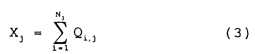


 the following observation equation is satisfied.


