EP1123993A2 - Single crystal SiC and method of growing the same - Google Patents
Single crystal SiC and method of growing the same Download PDFInfo
- Publication number
- EP1123993A2 EP1123993A2 EP01102504A EP01102504A EP1123993A2 EP 1123993 A2 EP1123993 A2 EP 1123993A2 EP 01102504 A EP01102504 A EP 01102504A EP 01102504 A EP01102504 A EP 01102504A EP 1123993 A2 EP1123993 A2 EP 1123993A2
- Authority
- EP
- European Patent Office
- Prior art keywords
- sic
- single crystal
- plate
- polycrystalline
- plane
- Prior art date
- Legal status (The legal status is an assumption and is not a legal conclusion. Google has not performed a legal analysis and makes no representation as to the accuracy of the status listed.)
- Withdrawn
Links
- 239000013078 crystal Substances 0.000 title claims abstract description 121
- 238000000034 method Methods 0.000 title claims description 32
- 229910010271 silicon carbide Inorganic materials 0.000 claims abstract description 87
- 239000000758 substrate Substances 0.000 claims abstract description 46
- 229910021431 alpha silicon carbide Inorganic materials 0.000 claims abstract description 41
- 238000010438 heat treatment Methods 0.000 claims abstract description 8
- 239000011261 inert gas Substances 0.000 claims abstract description 7
- VYPSYNLAJGMNEJ-UHFFFAOYSA-N Silicium dioxide Chemical compound O=[Si]=O VYPSYNLAJGMNEJ-UHFFFAOYSA-N 0.000 claims description 8
- 239000000463 material Substances 0.000 claims description 8
- 238000002230 thermal chemical vapour deposition Methods 0.000 claims description 8
- 239000000377 silicon dioxide Substances 0.000 claims description 4
- 229910052681 coesite Inorganic materials 0.000 claims description 3
- 229910052906 cristobalite Inorganic materials 0.000 claims description 3
- 239000000203 mixture Substances 0.000 claims description 3
- 229910052682 stishovite Inorganic materials 0.000 claims description 3
- 229910052905 tridymite Inorganic materials 0.000 claims description 3
- 230000007547 defect Effects 0.000 abstract description 6
- HBMJWWWQQXIZIP-UHFFFAOYSA-N silicon carbide Chemical compound [Si+]#[C-] HBMJWWWQQXIZIP-UHFFFAOYSA-N 0.000 description 36
- 238000005130 seeded sublimation method Methods 0.000 description 8
- 239000004065 semiconductor Substances 0.000 description 6
- 238000010586 diagram Methods 0.000 description 5
- 238000001953 recrystallisation Methods 0.000 description 5
- 230000008022 sublimation Effects 0.000 description 5
- 238000000859 sublimation Methods 0.000 description 5
- 238000000927 vapour-phase epitaxy Methods 0.000 description 4
- JBRZTFJDHDCESZ-UHFFFAOYSA-N AsGa Chemical compound [As]#[Ga] JBRZTFJDHDCESZ-UHFFFAOYSA-N 0.000 description 3
- 229910001218 Gallium arsenide Inorganic materials 0.000 description 3
- 239000007790 solid phase Substances 0.000 description 2
- OKTJSMMVPCPJKN-UHFFFAOYSA-N Carbon Chemical compound [C] OKTJSMMVPCPJKN-UHFFFAOYSA-N 0.000 description 1
- 238000002441 X-ray diffraction Methods 0.000 description 1
- 125000004429 atom Chemical group 0.000 description 1
- 229910052799 carbon Inorganic materials 0.000 description 1
- 125000004432 carbon atom Chemical group C* 0.000 description 1
- 229910003460 diamond Inorganic materials 0.000 description 1
- 239000010432 diamond Substances 0.000 description 1
- 230000000694 effects Effects 0.000 description 1
- 239000007789 gas Substances 0.000 description 1
- 239000012535 impurity Substances 0.000 description 1
- 230000003287 optical effect Effects 0.000 description 1
- 230000010287 polarization Effects 0.000 description 1
- 229910052710 silicon Inorganic materials 0.000 description 1
- 239000010703 silicon Substances 0.000 description 1
- 239000012808 vapor phase Substances 0.000 description 1
Images


Classifications
-
- C—CHEMISTRY; METALLURGY
- C30—CRYSTAL GROWTH
- C30B—SINGLE-CRYSTAL GROWTH; UNIDIRECTIONAL SOLIDIFICATION OF EUTECTIC MATERIAL OR UNIDIRECTIONAL DEMIXING OF EUTECTOID MATERIAL; REFINING BY ZONE-MELTING OF MATERIAL; PRODUCTION OF A HOMOGENEOUS POLYCRYSTALLINE MATERIAL WITH DEFINED STRUCTURE; SINGLE CRYSTALS OR HOMOGENEOUS POLYCRYSTALLINE MATERIAL WITH DEFINED STRUCTURE; AFTER-TREATMENT OF SINGLE CRYSTALS OR A HOMOGENEOUS POLYCRYSTALLINE MATERIAL WITH DEFINED STRUCTURE; APPARATUS THEREFOR
- C30B1/00—Single-crystal growth directly from the solid state
-
- C—CHEMISTRY; METALLURGY
- C30—CRYSTAL GROWTH
- C30B—SINGLE-CRYSTAL GROWTH; UNIDIRECTIONAL SOLIDIFICATION OF EUTECTIC MATERIAL OR UNIDIRECTIONAL DEMIXING OF EUTECTOID MATERIAL; REFINING BY ZONE-MELTING OF MATERIAL; PRODUCTION OF A HOMOGENEOUS POLYCRYSTALLINE MATERIAL WITH DEFINED STRUCTURE; SINGLE CRYSTALS OR HOMOGENEOUS POLYCRYSTALLINE MATERIAL WITH DEFINED STRUCTURE; AFTER-TREATMENT OF SINGLE CRYSTALS OR A HOMOGENEOUS POLYCRYSTALLINE MATERIAL WITH DEFINED STRUCTURE; APPARATUS THEREFOR
- C30B29/00—Single crystals or homogeneous polycrystalline material with defined structure characterised by the material or by their shape
- C30B29/10—Inorganic compounds or compositions
- C30B29/36—Carbides
Definitions
- the present invention relates to single crystal SiC and a method of growing the same, and more particularly to single crystal SiC which is used as a substrate wafer for a high temperature semiconductor electronic element such as a light-emitting diode, a rectifying element, a switching element, an amplifying element, and an optical sensor, and also to a method of growing the same.
- a high temperature semiconductor electronic element such as a light-emitting diode, a rectifying element, a switching element, an amplifying element, and an optical sensor, and also to a method of growing the same.
- Single crystal SiC (silicon carbide) is superior in heat resistance and mechanical strength. In addition, it is easy to perform the valence control of electrons and holes on single crystal SiC by doping an impurity. Moreover, single crystal SiC has a wide band gap (for example, single crystal 6H-SiC has a band gap of about 3.0 eV, and single crystal 4H-SiC has a band gap of 3.26 eV). For these reasons, it is possible to realize excellent high-temperature property, high-frequency property, dielectric property, and resistance to environments which cannot be attained by existing semiconductor materials such as Si (silicon) and GaAs (gallium arsenide). Therefore, single crystal SiC receives attention and is expected as a semiconductor material for a next-generation power device.
- the modified Lely method includes: a growing method which is most popularly used, and in which, as shown in Fig. 3, a single crystal a-SiC substrate 10 wherein (0 0 0 1) plane is exposed is used as a seed crystal, and single crystal SiC 11 is grown on (0 0 0 1) plane of the single crystal ⁇ -SiC substrate 10 by vapor phase epitaxy; and another method in which, as shown in Fig.
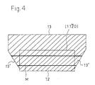
- a single crystal ⁇ -SiC substrate 12 wherein a face obtained by cutting along (1 1 2 0) Miller indices is exposed is used as a seed crystal, and single crystal SiC 13 is integrally grown on the exposed cut-off face of the single crystal ⁇ -SiC substrate 12 by vapor phase epitaxy.
- the crystal growth rate is as low as about 1 ⁇ m/hr.
- single crystal SiC which is obtained by the sublimation and recrystallization method contains many defects and cannot sufficiently satisfy requirements in quality.
- micropipes M which are produced in the single crystal ⁇ -SiC substrate 10 are transferred to the single crystal SiC 11 that is grown on the (0 0 0 1) plane of the single crystal ⁇ -SiC substrate 10, and then grown in the c-axis direction, whereby the quality is inevitably reduced.
- the single crystal SiC 11 grown on the (0 0 0 1) plane of the single crystal ⁇ -SiC substrate 10 is cut'along (1 1 2 0) Miller indices and then used as a wafer or the like. In this case, it is impossible to perform the cutting with an error of 0°. Moreover, not all of micropipes M elongate completely along the c-axis direction, and hence micropipes inevitably appear also in a wafer obtained by cutting, or the like.
- the invention has been conducted in view of the above-mentioned circumstances. It is an object of the invention to provide single crystal SiC of high quality to which influence of micropipes of a single crystal substrate is not transferred and a method of growing the same, thereby preventing distortion and micropipe defects from occurring.
- the single crystal SiC according to a first invention set forth in claim 1 is characterized in that heat treatment is performed in an inert gas atmosphere under a state where a cutting plane of a single crystal ⁇ -SiC substrate which is formed by cutting along (1 1 2 0) Miller index plane ⁇ 10°, and (2 2 0) Miller index plane of a polycrystalline ⁇ -SiC plate are superimposed on each other, whereby single crystal having a crystal orientation of an orientation of the cutting plane is integrally grown in the polycrystalline ⁇ -SiC plate in conformity with the single crystal ⁇ -SiC substrate.
- the method of growing single crystal SiC according to a second invention set forth in claim 3 is characterized in that, under a state where (2 2 0) Miller index plane of a polycrystalline ⁇ -SiC plate is superimposed on a cutting plane of a single crystal ⁇ -SiC substrate which is formed by cutting along (1 1 2 0) Miller index plane ⁇ 10°, the single crystal ⁇ -SiC substrate and the polycrystalline ⁇ -SiC plate are heat-treated in an inert gas atmosphere, whereby single crystal having a crystal orientation of an orientation of the cutting plane is integrally grown in the polycrystalline ⁇ -SiC plate in conformity with the single crystal ⁇ -SiC substrate.
- polycrystal which is produced in a plate-like form by the thermal chemical vapor deposition method (hereinafter, referred to as the thermal CVD method) is used as the polycrystalline ⁇ -SiC plate.
- the thermal CVD method thermal chemical vapor deposition method
- a polycrystalline ⁇ -SiC plate itself is of high purity and has no defects such as voids, grain boundaries or the like are not formed between the cutting plane of the single crystal ⁇ -SiC substrate and the (2 2 0) plane of the polycrystalline ⁇ -SiC plate, so that single crystal SiC of higher quality can be obtained.
- each of at least one cutting plane of the single crystal ⁇ -SiC substrate, and at least one (2 2 0) Miller index plane of the polycrystalline ⁇ -SiC plate may be processed into a smooth mirror face of 10 angstroms RMS or less. According to this configuration, the planes can be closely contacted with each other without leaving a gap therebetween. Therefore, single crystal SiC of high quality in which residual distortion and grain boundaries are not produced in the interface plane and which is substantially free from micropipe defects can be grown and supplied efficiently and stably on an industrial scale.
- Fig. 1 is a diagram showing a state where the single crystal SiC of the invention has not yet been heat-treated, i.e., the section structure of single crystal SiC according to a first invention.
- 1 denotes a single crystal hexagonal ⁇ -SiC substrate (6H type).
- a polycrystalline ⁇ -SiC plate 2 which is produced by the thermal CVD method and which has a thickness of 1 mm is superimposed on a cutting plane la or the surface of the substrate.
- the single crystal ⁇ -SiC substrate 1 is produced in the following manner. As shown in Fig. 2, single crystal ⁇ -SiC bulk 1' which is produced by the sublimation and recrystallization method or the like is cut by a diamond cutter along (1 1 2 0) Miller index plane ⁇ 1°, into a plate-like shape having a thickness (tl) of 0.5 mm. The front and rear faces of the cut-off single crystal ⁇ -SiC substrate 1 are polished by about 50 ⁇ m, and the one cutting plane la is processed into a smooth mirror face of 10 angstroms RMS or less.
- (2 2 0) Miller index plane 2a of the polycrystalline ⁇ -SiC plate 2 which is produced by the thermal CVD method, and which has a thickness of 1 mm is polished, and the polished (2 2 0) plane 2a is processed into a smooth mirror face of 10 angstroms RMS or less.
- the cutting plane la consisting of the smooth mirror face of the single crystal ⁇ -SiC substrate 1, and the (2 2 0) Miller index plane 2a consisting of the smooth mirror face of the polycrystalline ⁇ -SiC plate 2 are superimposed on each other.
- the superimposed members are placed in a high-temperature electric oven using a carbon heater, and Ar gas is blown into the oven to attain an inert gas atmosphere. Under this atmosphere, the substrate 1 and the plate 2 are heated at an average rate at which the temperature is raised from 1,100°C to 2,200 ⁇ 100°C over 30 minutes, and the temperature of 2,200 ⁇ 100°C is maintained for one hour.
- the inventors conducted crystal X-ray analysis using an X-ray diffractometer on samples of the single crystal SiC which were grown in the manner described above. As a result, it was confirmed that the single crystal portion 4 grown in the polycrystalline ⁇ -SiC plate 2 is single crystal ⁇ -(6H)-SiC which has the crystal orientation of the orientation of (1 1 2 0) in conformity with the single crystal ⁇ -SiC substrate 1.
- samples of the single crystal SiC were observed by a polarization microscope. As a result, it was confirmed that no micropipes M are produced in the single crystal portion 4 grown in the polycrystalline ⁇ -SiC plate 2. Evenness of crystal was shown from observation by a Lang camera. Therefore, it was confirmed that the samples were single crystal SiC of high quality.
- a thin layer configured by SiO 2 (silica), Si, or a mixture of these materials may be interposed in the superimposed portion of the cutting plane la of the single crystal ⁇ -SiC substrate 1 and the (2 2 0) Miller index plane 2a of the polycrystalline ⁇ -SiC plate 2.
Landscapes
- Chemical & Material Sciences (AREA)
- Engineering & Computer Science (AREA)
- Crystallography & Structural Chemistry (AREA)
- Materials Engineering (AREA)
- Metallurgy (AREA)
- Organic Chemistry (AREA)
- Inorganic Chemistry (AREA)
- Crystals, And After-Treatments Of Crystals (AREA)
Abstract
In the single crystal SiC according to the invention,
heat treatment is performed in an inert gas atmosphere under
a state where a cutting plane of a single crystal α-SiC substrate
which is produced in a plate-like form by cutting along
(1 1 2 0) Miller index plane ± 10°, and (2 2 0) Miller index
plane of a polycrystalline β-SiC plate are superimposed on
each other, whereby single crystal having a crystal orientation
of an orientation of the cutting plane is integrally
grown in the polycrystalline β-SiC plate in conformity with
the single crystal α-SiC substrate. According to this configuration,
single crystal SiC of very high quality is obtained
to which influence of micropipes of the single crystal
α-SiC substrate is not transferred, thereby preventing distortion
and micropipe defects from occurring.
Description
- The present invention relates to single crystal SiC and a method of growing the same, and more particularly to single crystal SiC which is used as a substrate wafer for a high temperature semiconductor electronic element such as a light-emitting diode, a rectifying element, a switching element, an amplifying element, and an optical sensor, and also to a method of growing the same.
- Single crystal SiC (silicon carbide) is superior in heat resistance and mechanical strength. In addition, it is easy to perform the valence control of electrons and holes on single crystal SiC by doping an impurity. Moreover, single crystal SiC has a wide band gap (for example, single crystal 6H-SiC has a band gap of about 3.0 eV, and single crystal 4H-SiC has a band gap of 3.26 eV). For these reasons, it is possible to realize excellent high-temperature property, high-frequency property, dielectric property, and resistance to environments which cannot be attained by existing semiconductor materials such as Si (silicon) and GaAs (gallium arsenide). Therefore, single crystal SiC receives attention and is expected as a semiconductor material for a next-generation power device.
- As a method of growing single crystal SiC of this type, conventionally, well known is the modified Lely method in which single crystal SiC is grown by the sublimation and recrystallization method using a seed crystal. The modified Lely method includes: a growing method which is most popularly used, and in which, as shown in Fig. 3, a single crystal a-SiC
substrate 10 wherein (0 0 0 1) plane is exposed is used as a seed crystal, andsingle crystal SiC 11 is grown on (0 0 0 1) plane of the single crystal α-SiC substrate 10 by vapor phase epitaxy; and another method in which, as shown in Fig. 4, a single crystal α-SiC substrate 12 wherein a face obtained by cutting along (1 12 0) Miller indices is exposed is used as a seed crystal, andsingle crystal SiC 13 is integrally grown on the exposed cut-off face of the single crystal α-SiC substrate 12 by vapor phase epitaxy. - In both the above-mentioned growing methods according to the modified Lely method, the crystal growth rate is as low as about 1 µm/hr., and single crystal SiC which is obtained by the sublimation and recrystallization method contains many defects and cannot sufficiently satisfy requirements in quality. In single crystal SiC which is grown by the usual modified Lely method shown in Fig. 3, particularly, micropipes M which are produced in the single crystal α-
SiC substrate 10 are transferred to thesingle crystal SiC 11 that is grown on the (0 0 0 1) plane of the single crystal α-SiC substrate 10, and then grown in the c-axis direction, whereby the quality is inevitably reduced. In order to suppress such reduction of quality, it may be contemplated that thesingle crystal SiC 11 grown on the (0 0 0 1) plane of the single crystal α-SiC substrate 10 is cut'along (1 12 0) Miller indices and then used as a wafer or the like. In this case, it is impossible to perform the cutting with an error of 0°. Moreover, not all of micropipes M elongate completely along the c-axis direction, and hence micropipes inevitably appear also in a wafer obtained by cutting, or the like. - By contrast, in the growing method based on the modified Lely method shown in Fig. 4, vapor phase bulk growth is conducted, and therefore the crystal is additionally grown not only on an exposed cut-off face of a single crystal α-SiC substrate but also-in lateral directions of a single crystal SiC portion 13'. As a result, micropipes M which are produced in the single crystal α-
SiC substrate 12 are transferred also to the single crystal SiC portion 13' which is laterally grown. Therefore, the grownsingle crystal SiC 13 is inevitably formed as an incomplete crystal or a product of a low quality in which micropipe defects are produced. Consequently, single crystal SiC which is grown by any of conventional modified Lely methods is blocked from being practically used, although such single crystal SiC has many features more excellent than existing semiconductor materials such as Si and GaAs as described above. - The invention has been conducted in view of the above-mentioned circumstances. It is an object of the invention to provide single crystal SiC of high quality to which influence of micropipes of a single crystal substrate is not transferred and a method of growing the same, thereby preventing distortion and micropipe defects from occurring.
- In order to attain the above-mentioned object, the single crystal SiC according to a first invention set forth in
claim 1 is characterized in that heat treatment is performed in an inert gas atmosphere under a state where a cutting plane of a single crystal α-SiC substrate which is formed by cutting along (1 12 0) Miller index plane ± 10°, and (2 2 0) Miller index plane of a polycrystalline β-SiC plate are superimposed on each other, whereby single crystal having a crystal orientation of an orientation of the cutting plane is integrally grown in the polycrystalline β-SiC plate in conformity with the single crystal α-SiC substrate. - The method of growing single crystal SiC according to a second invention set forth in
claim 3 is characterized in that, under a state where (2 2 0) Miller index plane of a polycrystalline β-SiC plate is superimposed on a cutting plane of a single crystal α-SiC substrate which is formed by cutting along (1 12 0) Miller index plane ± 10°, the single crystal α-SiC substrate and the polycrystalline β-SiC plate are heat-treated in an inert gas atmosphere, whereby single crystal having a crystal orientation of an orientation of the cutting plane is integrally grown in the polycrystalline β-SiC plate in conformity with the single crystal α-SiC substrate. - In the thus configured first and second inventions set forth in
claims 2 0) Miller index plane ± 10° of the single crystal α-SiC substrate, and the (2 2 0) Miller index plane of the polycrystalline β-SiC plate, and heat treatment is then conducted in an inert gas atmosphere. As a result, solid phase growth in which the whole region of the interface plane of the polycrystalline β-SiC plate is converted substantially simultaneously and rapidly to α-SiC can be performed. Therefore, it is possible to grow single crystal which is free not only micropipes but also from distortion and residual grain boundaries due to uneven crystal growth rates, so that single crystal SiC of very high quality can be obtained. Consequently, it is possible to attain an effect of expediting practical use of single crystal SiC which has excellent high-temperature property, high-frequency property, dielectric property, and resistance to environments as compared with existing semiconductor materials, and which is therefore expected as a semiconductor material for a next-generation power device. - Preferably, polycrystal which is produced in a plate-like form by the thermal chemical vapor deposition method (hereinafter, referred to as the thermal CVD method) is used as the polycrystalline β-SiC plate. In this case, since a polycrystalline β-SiC plate itself is of high purity and has no defects such as voids, grain boundaries or the like are not formed between the cutting plane of the single crystal α-SiC substrate and the (2 2 0) plane of the polycrystalline β-SiC plate, so that single crystal SiC of higher quality can be obtained.
- In the method of growing single crystal SiC according to the second invention set forth in
claim 3, each of at least one cutting plane of the single crystal α-SiC substrate, and at least one (2 2 0) Miller index plane of the polycrystalline β-SiC plate may be processed into a smooth mirror face of 10 angstroms RMS or less. According to this configuration, the planes can be closely contacted with each other without leaving a gap therebetween. Therefore, single crystal SiC of high quality in which residual distortion and grain boundaries are not produced in the interface plane and which is substantially free from micropipe defects can be grown and supplied efficiently and stably on an industrial scale. -
- Fig. 1 is a diagram showing the section structure of single crystal SiC according to a first invention;
- Fig. 2 is a diagram illustrating Miller index planes of a single crystal α-SiC substrate which is used in first and second inventions;
- Fig. 3 is a diagram showing the modified Lely method which, among conventional sublimation and recrystallization methods, is most popularly used for growing single crystal SiC by vapor phase epitaxy on (0 0 0 1) plane of a single crystal α-SiC substrate; and
- Fig. 4 is a diagram showing the modified Lely method
which, among conventional sublimation and recrystallization
methods, is used for integrally growing single crystal SiC by
vapor phase epitaxy on an exposed cut-off face of a single
crystal α-SiC substrate wherein a face obtained by cutting
along (1 1
2 0) Miller indices is exposed. -
- Hereinafter, an embodiment of the invention will be described with reference to the drawings.
- Fig. 1 is a diagram showing a state where the single crystal SiC of the invention has not yet been heat-treated, i.e., the section structure of single crystal SiC according to a first invention. In Fig. 1, 1 denotes a single crystal hexagonal α-SiC substrate (6H type). A polycrystalline β-
SiC plate 2 which is produced by the thermal CVD method and which has a thickness of 1 mm is superimposed on a cutting plane la or the surface of the substrate. - The single crystal α-
SiC substrate 1 is produced in the following manner. As shown in Fig. 2, single crystal α-SiC bulk 1' which is produced by the sublimation and recrystallization method or the like is cut by a diamond cutter along (1 1 2 0) Miller index plane ± 1°, into a plate-like shape having a thickness (tl) of 0.5 mm. The front and rear faces of the cut-off single crystal α-SiC substrate 1 are polished by about 50 µm, and the one cutting plane la is processed into a smooth mirror face of 10 angstroms RMS or less. - On the other hand, (2 2 0) Miller
index plane 2a of the polycrystalline β-SiC plate 2 which is produced by the thermal CVD method, and which has a thickness of 1 mm is polished, and the polished (2 2 0)plane 2a is processed into a smooth mirror face of 10 angstroms RMS or less. - Then, the cutting plane la consisting of the smooth mirror face of the single crystal α-
SiC substrate 1, and the (2 2 0) Millerindex plane 2a consisting of the smooth mirror face of the polycrystalline β-SiC plate 2 are superimposed on each other. The superimposed members are placed in a high-temperature electric oven using a carbon heater, and Ar gas is blown into the oven to attain an inert gas atmosphere. Under this atmosphere, thesubstrate 1 and theplate 2 are heated at an average rate at which the temperature is raised from 1,100°C to 2,200 ± 100°C over 30 minutes, and the temperature of 2,200 ± 100°C is maintained for one hour. As a result of this heat treatment, solid-phase growth occurs in theinterface plane 3 between the cutting plane la of the single crystal a-SiCsubstrate 1 and the (2 2 0) Millerindex plane 2a of the polycrystalline β-SiC plate 2, so that asingle crystal portion 4 which has the crystal orientation of the orientation of the cutting plane la in conformity with the single crystal a-SiCsubstrate 1, and which is approximately colorless and transparent is grown integrally in the polycrystalline β-SiC plate 2 and over the whole region of theinterface plane 3. - The inventors conducted crystal X-ray analysis using an X-ray diffractometer on samples of the single crystal SiC which were grown in the manner described above. As a result, it was confirmed that the
single crystal portion 4 grown in the polycrystalline β-SiC plate 2 is single crystal α-(6H)-SiC which has the crystal orientation of the orientation of (1 12 0) in conformity with the single crystal α-SiC substrate 1. - Moreover, samples of the single crystal SiC were observed by a polarization microscope. As a result, it was confirmed that no micropipes M are produced in the
single crystal portion 4 grown in the polycrystalline β-SiC plate 2. Evenness of crystal was shown from observation by a Lang camera. Therefore, it was confirmed that the samples were single crystal SiC of high quality. - Alternatively, a thin layer configured by SiO2 (silica), Si, or a mixture of these materials may be interposed in the superimposed portion of the cutting plane la of the single crystal α-
SiC substrate 1 and the (2 2 0) Millerindex plane 2a of the polycrystalline β-SiC plate 2. - The entire disclosure of Japanese Patent Application No. 2000-030763 filed on February 8, 2000 including specification, claims, drawings, and summary are incorporated herein by reference in its entirety.
Claims (10)
- Single crystal SiC wherein
heat treatment is performed in an inert gas atmosphere under a state where a cutting plane of a single crystal α-SiC substrate which is formed by cutting along (1 12 0) Miller index plane ± 10°, and (2 2 0) Miller index plane of a polycrystalline β-SiC plate are superimposed on each other, whereby single crystal having a crystal orientation of an orientation of said cutting plane is integrally grown in said polycrystalline β-SiC plate in conformity with said single crystal α-SiC substrate. - Single crystal SiC according to claim 1, wherein polycrystal which is produced in a plate-like form by a thermal chemical vapor deposition method is used as said polycrystalline β-SiC plate.
- A method of growing single crystal SiC in which heat treatment is performed while superimposing a single crystal α-SiC substrate and a polycrystalline β-SiC plate, wherein under a state where (2 2 0) Miller index plane of said β-SiC plate is superimposed on a cutting plane of said single crystal α-SiC substrate which is formed by cutting along (1 1
2 0) Miller index plane ± 10°, said single crystal α-SiC substrate and said polycrystalline β-SiC plate which are superimposed on each other are heat-treated in an inert gas atmosphere, whereby single crystal having a crystal orientation of an orientation of said cutting plane is integrally grown in said polycrystalline β-SiC plate in conformity with said single crystal α-SiC substrate. - A method of growing single crystal SiC according to claim 3, wherein polycrystal which is produced in a plate-like form by a thermal chemical vapor deposition method is used as said polycrystalline β-SiC plate.
- A method of growing single crystal SiC according to claim 3, wherein each of at least one cutting plane of said single crystal α-SiC substrate, and at least one (2 2 0) Miller index plane of said polycrystalline β-SiC plate is processed into a smooth mirror face of 10 angstroms RMS or less.
- A method of growing single crystal SiC according to claim 4, wherein each of at least one cutting plane of said single crystal α-SiC substrate, and at least one (2 2 0) Miller index plane of said polycrystalline β-SiC plate which is produced in a plate-like form by the thermal chemical vapor deposition method is processed into a smooth mirror face of 10 angstroms RMS or less.
- A method of growing single crystal SiC according to claim 3, wherein a thin layer configured by SiO2, Si, or a mixture of these materials is interposed in a superimposed portion of said cutting plane of said single crystal α-SiC substrate and said (2 2 0) Miller index plane of said polycrystalline β-SiC plate.
- A method of growing single crystal SiC according to claim 4, wherein a thin layer configured by SiO2, Si, or a mixture of these materials is interposed in a superimposed portion of said cutting plane of said single crystal α-SiC substrate and (2 2 0) Miller index plane of said polycrystalline β-SiC plate which is produced in a plate-like form by the thermal chemical vapor deposition method.
- A method of growing single crystal SiC according to claim 3, wherein a temperature of said heat treatment is set to be in a range of 2,100 to 2,300°C.
- A method of growing single crystal SiC according to claim 4, wherein a temperature of said heat treatment is set to be in a range of 2,100 to 2,300°C.
Applications Claiming Priority (2)
| Application Number | Priority Date | Filing Date | Title |
|---|---|---|---|
| JP2000030763A JP2001220297A (en) | 2000-02-08 | 2000-02-08 | Single crystal SiC and method for growing the same |
| JP2000030763 | 2000-02-08 |
Publications (1)
| Publication Number | Publication Date |
|---|---|
| EP1123993A2 true EP1123993A2 (en) | 2001-08-16 |
Family
ID=18555738
Family Applications (1)
| Application Number | Title | Priority Date | Filing Date |
|---|---|---|---|
| EP01102504A Withdrawn EP1123993A2 (en) | 2000-02-08 | 2001-02-05 | Single crystal SiC and method of growing the same |
Country Status (3)
| Country | Link |
|---|---|
| US (1) | US20010011519A1 (en) |
| EP (1) | EP1123993A2 (en) |
| JP (1) | JP2001220297A (en) |
-
2000
- 2000-02-08 JP JP2000030763A patent/JP2001220297A/en active Pending
-
2001
- 2001-01-30 US US09/771,556 patent/US20010011519A1/en not_active Abandoned
- 2001-02-05 EP EP01102504A patent/EP1123993A2/en not_active Withdrawn
Also Published As
| Publication number | Publication date |
|---|---|
| US20010011519A1 (en) | 2001-08-09 |
| JP2001220297A (en) | 2001-08-14 |
Similar Documents
| Publication | Publication Date | Title |
|---|---|---|
| EP1807557B1 (en) | Monocrystalline silicon carbide ingot, monocrystalline silicon carbide wafer and method of manufacturing the same | |
| JP4979579B2 (en) | Silicon carbide growth system and seed crystal sublimation method for growing silicon carbide large single crystals | |
| JP2804860B2 (en) | SiC single crystal and growth method thereof | |
| US5248385A (en) | Process for the homoepitaxial growth of single-crystal silicon carbide films on silicon carbide wafers | |
| EP0916750A1 (en) | Single crystal SiC and a method of producing the same | |
| EP1657740B1 (en) | Silicon carbide epitaxial wafer, method for producing such wafer, and semiconductor device formed on such wafer | |
| KR100773624B1 (en) | Seed crystal consisting of silicon carbide single crystal and method for producing ingot using same | |
| KR20110071092A (en) | Silicon Carbide Monocrystalline and Silicon Carbide Monocrystalline Wafers | |
| WO2015182474A1 (en) | Silicon-carbide-ingot manufacturing method, silicon-carbide seed substrate, silicon-carbide substrate, semiconductor device, and semiconductor-device manufacturing method | |
| EP0069206B1 (en) | Single crystals of xsic.(1-x)aln | |
| EP0964081B1 (en) | Method of producing a single crystal of SiC | |
| CN110872731B (en) | N-type 4H-SiC single crystal substrate and method for producing n-type 4H-SiC single crystal substrate | |
| EP0921214B1 (en) | Single crystal silicon carbide and process for preparing the same | |
| JP2024522507A (en) | Reduction of optical absorption for silicon carbide crystalline materials | |
| JP4253974B2 (en) | SiC single crystal and growth method thereof | |
| EP1122341A1 (en) | Single crystal SiC | |
| EP1130137B1 (en) | Material for raising single crystal sic and method of preparing single crystal sic | |
| JP3487254B2 (en) | Single crystal SiC and method for producing the same | |
| EP0964084A1 (en) | SINGLE CRYSTAL SiC AND PROCESS FOR PREPARING THE SAME | |
| JP3848446B2 (en) | Method for growing low resistance SiC single crystal | |
| Ohtani et al. | Development of large single‐crystal SiC substrates | |
| JP3254557B2 (en) | Single crystal SiC and method for producing the same | |
| JP4157326B2 (en) | 4H type silicon carbide single crystal ingot and wafer | |
| US20010011519A1 (en) | Single crystal SiC and a method of growing the same | |
| JP3087030B2 (en) | SiC composite, method for producing the same, and single crystal SiC |
Legal Events
| Date | Code | Title | Description |
|---|---|---|---|
| PUAI | Public reference made under article 153(3) epc to a published international application that has entered the european phase |
Free format text: ORIGINAL CODE: 0009012 |
|
| AK | Designated contracting states |
Kind code of ref document: A2 Designated state(s): AT BE CH CY DE DK ES FI FR GB GR IE IT LI LU MC NL PT SE TR |
|
| AX | Request for extension of the european patent |
Free format text: AL;LT;LV;MK;RO;SI |
|
| RAP1 | Party data changed (applicant data changed or rights of an application transferred) |
Owner name: NISSIN ELECTRIC CO., LTD. |
|
| STAA | Information on the status of an ep patent application or granted ep patent |
Free format text: STATUS: THE APPLICATION IS DEEMED TO BE WITHDRAWN |
|
| 18D | Application deemed to be withdrawn |
Effective date: 20050901 |