EP1122922A1 - Line driver with adaptive output impedance - Google Patents
Line driver with adaptive output impedance Download PDFInfo
- Publication number
- EP1122922A1 EP1122922A1 EP01300323A EP01300323A EP1122922A1 EP 1122922 A1 EP1122922 A1 EP 1122922A1 EP 01300323 A EP01300323 A EP 01300323A EP 01300323 A EP01300323 A EP 01300323A EP 1122922 A1 EP1122922 A1 EP 1122922A1
- Authority
- EP
- European Patent Office
- Prior art keywords
- current
- circuit
- buffer
- signal
- output
- Prior art date
- Legal status (The legal status is an assumption and is not a legal conclusion. Google has not performed a legal analysis and makes no representation as to the accuracy of the status listed.)
- Granted
Links
Images






Classifications
-
- H—ELECTRICITY
- H04—ELECTRIC COMMUNICATION TECHNIQUE
- H04L—TRANSMISSION OF DIGITAL INFORMATION, e.g. TELEGRAPHIC COMMUNICATION
- H04L25/00—Baseband systems
- H04L25/02—Details ; arrangements for supplying electrical power along data transmission lines
- H04L25/0264—Arrangements for coupling to transmission lines
- H04L25/0266—Arrangements for providing Galvanic isolation, e.g. by means of magnetic or capacitive coupling
-
- H—ELECTRICITY
- H04—ELECTRIC COMMUNICATION TECHNIQUE
- H04L—TRANSMISSION OF DIGITAL INFORMATION, e.g. TELEGRAPHIC COMMUNICATION
- H04L25/00—Baseband systems
- H04L25/02—Details ; arrangements for supplying electrical power along data transmission lines
- H04L25/0264—Arrangements for coupling to transmission lines
- H04L25/0278—Arrangements for impedance matching
-
- H—ELECTRICITY
- H04—ELECTRIC COMMUNICATION TECHNIQUE
- H04L—TRANSMISSION OF DIGITAL INFORMATION, e.g. TELEGRAPHIC COMMUNICATION
- H04L25/00—Baseband systems
- H04L25/02—Details ; arrangements for supplying electrical power along data transmission lines
- H04L25/0264—Arrangements for coupling to transmission lines
- H04L25/028—Arrangements specific to the transmitter end
-
- H—ELECTRICITY
- H04—ELECTRIC COMMUNICATION TECHNIQUE
- H04L—TRANSMISSION OF DIGITAL INFORMATION, e.g. TELEGRAPHIC COMMUNICATION
- H04L25/00—Baseband systems
- H04L25/02—Details ; arrangements for supplying electrical power along data transmission lines
- H04L25/0264—Arrangements for coupling to transmission lines
- H04L25/0272—Arrangements for coupling to multiple lines, e.g. for differential transmission
Definitions
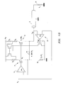
- one half of the push-pull circuit i.e., one driver 10
- one driver When one half of the push-pull circuit (i.e., one driver 10) generates some voltage in one half of the primary coil of the transformer, a flyback voltage appears in the other half of the primary coil. This flyback voltage penetrates to the input of the operational amplifier 12 of the other driver 10 through the feedback circuit connections and corrupts driver operation.
Landscapes
- Engineering & Computer Science (AREA)
- Power Engineering (AREA)
- Computer Networks & Wireless Communication (AREA)
- Signal Processing (AREA)
- Logic Circuits (AREA)
- Amplifiers (AREA)
- Control Of Electrical Variables (AREA)
- Dc Digital Transmission (AREA)
Abstract
Description
G(source 52(1))=gin; and
G(source 52(2))=gin*Rin/(N+1)RL,
wherein gin is the transconductance of the input signal source and Rin is the resistance value for the
Claims (17)
- A line driver circuit, comprising:a buffer including an adjustable current source and having a signal input and a signal output that provides a line driver output signal buffered from the signal input, the buffer further including a tuning input connected to the adjustable current source; anda tuning circuit, comprising:a first current source producing a first current;a second current source producing a second current;a current mirror having a fixed branch connected to receive the first current and an adjustable branch connected to receive the second current, the current mirror further having a control input to the adjustable branch and having an output; anda comparison circuit receiving the current mirror output for comparison to predetermined limits, the comparison circuit generating a control signal for application to the control input to maintain the current mirror output within the predetermined limits and generating a tuning signal for application to the tuning input of the buffer to adjust operation of the adjustable
- A line driver circuit for connection to a transformer having a primary coil, comprising:a pair of equivalent controlled impedance buffers for connection in a push-pull configuration to the primary coil, each buffer receiving a buffer input signal for buffered output as a line driver signal to the primary coil, each buffer further including a tuning input connected to an adjustable current source whose operation effectuates control over buffer output impedance; anda tuning circuit that generates a tuning signal for application to the tuning input of each buffer to adjust operation of the adjustable current source to control the buffer output impedance.
- The circuit of claim 1 or claim 2 wherein the line driver signal is applied through the transformer to a transmission line having a characteristic impedance, and wherein the tuning signal that adjusts operation of the adjustable current source controls the output impedance of the buffer to substantially match the characteristic impedance of the transmission line.
- The circuit of claim 3 wherein the buffer is connected to the transmission line through a transformer.
- The circuit of claim 1 or claim 2 wherein the tuning signal that adjusts operation of the adjustable current source controls each buffer gain to provide substantially unity gain.
- The circuit of claim 2 wherein the tuning circuit comprises:a first current source producing a first current;a second current source producing a second current;a current mirror having a fixed branch connected to receive the first current and an adjustable branch connected to receive the second current, the current mirror further having a control input to the adjustable branch and having an output; anda comparison circuit receiving the current mirror output for comparison to predetermined limits, the comparison circuit generating a control signal for application to the control input of the adjustable branch to maintain the control mirror output within the predetermined limits and generating the tuning signal for application to the tuning input of the buffer to adjust operation of the adjustable current source to control the output impedance of the buffer.
- The circuit of claim 1 or claim 6 wherein the first current source generates the first current derived from the value of a first resistor and the second current source generates the second current derived from the value of a second resistor.
- The circuit of claim 7 wherein the line driver circuit is fabricated on an integrated circuit and the first resistor comprises a stable precise resistor external to the integrated circuit and the second resistor comprises a resistor fabricated on the integrated circuit.
- The circuit of claim 1 or claim 6 wherein the comparison circuit comprises an analog-to-digital converter that generates a digital signal representative of whether the adjustable branch output is within the predetermined limits, the digital signal applied as the control signal to the control input to maintain the current mirror output within the predetermined limits.
- The circuit of claim 9 wherein the adjustable branch of the current mirror includes at least one current path, and the control input comprising the digital signal turns on and off that current path.
- The circuit of claim 1 or claim 6 wherein the comparison circuit comprises an analog signal generator that generates a analog signal representative of the current mirror output, the analog signal applied as the control signal to the control input to the control the current mirror output.
- The circuit of claim 11 wherein the adjustable branch of the current mirror includes at least one current path, and the control input comprising the analog signal controls current flowing through that current path.
- A method for controlling the output impedance of a line driver, comprising the steps of:generating a first and second currents;applying the first current to a fixed branch of a current mirror circuit;applying the second current to an adjustable branch of the current mirror circuit;comparing an output from the current mirror circuit to some predetermined limits to generate a control signal;applying the control signal to the adjustable branch of the current mirror circuit to maintain the current mirror output within the predetermined limits;applying the same control signal to an adjustable current source within the line driver to maintain an output impedance of the line driver in a substantially matching condition to a driven transmission line.
- The method as in claim 13 wherein the step of generating comprises the steps of:deriving the first current from the value of a first resistor; andderiving the second current from the value of a second resistor.
- The method as in claim 14 wherein the line driver comprises an integrated circuit line driver, the first resistor comprises a stable precise resistor external to the integrated circuit, and the second resistor comprises a resistor fabricated on the integrated circuit.
- The method as in claim 13 wherein the control signal comprises a digital signal, and the step of applying the control signal to the adjustable branch of the current mirror circuit comprises the step of turning a current path of the adjustable branch on and off.
- The method as in claim 13 wherein the control signal comprises an analog signal, and the step of applying the control signal to the adjustable branch of the current mirror circuit comprises the step of adjusting the flow of current through a current path of the adjustable branch in response to the analog signal.
Applications Claiming Priority (2)
| Application Number | Priority Date | Filing Date | Title |
|---|---|---|---|
| US497980 | 2000-02-04 | ||
| US09/497,980 US6275078B1 (en) | 2000-02-04 | 2000-02-04 | Self-adjustable impendance line driver |
Publications (2)
| Publication Number | Publication Date |
|---|---|
| EP1122922A1 true EP1122922A1 (en) | 2001-08-08 |
| EP1122922B1 EP1122922B1 (en) | 2003-08-20 |
Family
ID=23979116
Family Applications (1)
| Application Number | Title | Priority Date | Filing Date |
|---|---|---|---|
| EP01300323A Expired - Lifetime EP1122922B1 (en) | 2000-02-04 | 2001-01-16 | Line driver with adaptive output impedance |
Country Status (4)
| Country | Link |
|---|---|
| US (1) | US6275078B1 (en) |
| EP (1) | EP1122922B1 (en) |
| JP (1) | JP2001268138A (en) |
| DE (1) | DE60100605T2 (en) |
Cited By (2)
| Publication number | Priority date | Publication date | Assignee | Title |
|---|---|---|---|---|
| FR2905211A1 (en) * | 2006-08-22 | 2008-02-29 | St Microelectronics Sa | Transmitter i.e. processor, output impedance matching method for communication device, involves sending control signal, based on comparison signal, to programmable resistive element to reduce gap between reference and measurement voltages |
| EP2186191A4 (en) * | 2007-09-06 | 2011-04-20 | Catena Wireless Electronics Inc | Method of using integrated power amplifier |
Families Citing this family (8)
| Publication number | Priority date | Publication date | Assignee | Title |
|---|---|---|---|---|
| US6542008B1 (en) * | 2000-11-28 | 2003-04-01 | Agere Systems Inc. | System and method for providing an impedance match of an output buffer to a transmission line |
| US6498521B1 (en) * | 2001-11-29 | 2002-12-24 | Lsi Logic Corporation | Dynamic supply control for line driver |
| US20050213783A1 (en) * | 2004-03-29 | 2005-09-29 | Walsh William J | Transmission drive line for low level audio analog electrical signals |
| CN1306703C (en) * | 2004-04-30 | 2007-03-21 | 华为技术有限公司 | Line driver and output signal controlling method thereof |
| US7609097B2 (en) * | 2004-07-06 | 2009-10-27 | Agere Systems, Inc. | Driver circuit and a method for matching the output impedance of a driver circuit with a load impedance |
| CN100476680C (en) * | 2006-04-18 | 2009-04-08 | 点晶科技股份有限公司 | Automatic shifting current mirror |
| US8150074B1 (en) * | 2008-08-08 | 2012-04-03 | Crestron Electronics Inc. | Impedance matching speaker wire system |
| TWI559682B (en) | 2015-01-14 | 2016-11-21 | 智原科技股份有限公司 | Driving circuit, driving apparatus, and method for adjusting output impedance to match transmission line impedance by current adjusting |
Citations (5)
| Publication number | Priority date | Publication date | Assignee | Title |
|---|---|---|---|---|
| US5585763A (en) * | 1995-03-30 | 1996-12-17 | Crystal Semiconductor Corporation | Controlled impedance amplifier |
| US5631595A (en) * | 1994-09-30 | 1997-05-20 | Lucent Technologies Inc. | Voltage signal line driver comprising a push-pull bridge amplifier |
| US5760601A (en) * | 1996-08-26 | 1998-06-02 | International Business Machines Corporation | Transmission line driver circuit for matching transmission line characteristic impedance |
| WO1998038773A2 (en) * | 1997-02-25 | 1998-09-03 | Koninklijke Philips Electronics N.V. | Line driver with adaptive output impedance |
| WO1998038774A2 (en) * | 1997-02-25 | 1998-09-03 | Koninklijke Philips Electronics N.V. | Line driver with adaptive output impedance |
Family Cites Families (14)
| Publication number | Priority date | Publication date | Assignee | Title |
|---|---|---|---|---|
| NL8602325A (en) | 1986-09-15 | 1988-04-05 | Philips Nv | ACTIVE SYMMETRICAL BALANCE FORK SWITCH. |
| US5121080A (en) | 1990-12-21 | 1992-06-09 | Crystal Semiconductor Corporation | Amplifier with controlled output impedance |
| US5249225A (en) * | 1991-10-25 | 1993-09-28 | Coherent Communications Systems Corp. | Self-balancing hybrid using digitally programmable attenuator for variable impedance elements |
| US5285744A (en) * | 1992-09-04 | 1994-02-15 | Vapor Systems Technologies, Inc. | Coaxial hose assembly |
| GB9308168D0 (en) | 1993-04-20 | 1993-06-02 | Madge Network Limited | Impedance matching |
| TW239239B (en) * | 1993-07-14 | 1995-01-21 | Philips Electronics Nv | |
| US6107867A (en) * | 1994-09-30 | 2000-08-22 | Lucent Technologies Inc. | Load termination sensing circuit |
| US5796276A (en) * | 1994-12-30 | 1998-08-18 | Sgs-Thomson Microelectronics, Inc. | High-side-driver gate drive circuit |
| US5585732A (en) | 1995-06-07 | 1996-12-17 | Mississippi State University | Detector for heterogeneous materials |
| US5757210A (en) * | 1995-08-30 | 1998-05-26 | Cherry Semiconductor Corporation | Comparator with latch |
| US5644258A (en) * | 1996-01-04 | 1997-07-01 | Winbond Electronics Corp. | Driver circuit, with low idle power consumption, for an attachment unit interface |
| US5793223A (en) * | 1996-08-26 | 1998-08-11 | International Business Machines Corporation | Reference signal generation in a switched current source transmission line driver/receiver system |
| US5936393A (en) | 1997-02-25 | 1999-08-10 | U.S. Philips Corporation | Line driver with adaptive output impedance |
| US5973490A (en) | 1997-02-25 | 1999-10-26 | U.S. Philips Corporation | Line driver with adaptive output impedance |
-
2000
- 2000-02-04 US US09/497,980 patent/US6275078B1/en not_active Expired - Lifetime
-
2001
- 2001-01-16 EP EP01300323A patent/EP1122922B1/en not_active Expired - Lifetime
- 2001-01-16 DE DE60100605T patent/DE60100605T2/en not_active Expired - Fee Related
- 2001-02-05 JP JP2001028614A patent/JP2001268138A/en active Pending
Patent Citations (5)
| Publication number | Priority date | Publication date | Assignee | Title |
|---|---|---|---|---|
| US5631595A (en) * | 1994-09-30 | 1997-05-20 | Lucent Technologies Inc. | Voltage signal line driver comprising a push-pull bridge amplifier |
| US5585763A (en) * | 1995-03-30 | 1996-12-17 | Crystal Semiconductor Corporation | Controlled impedance amplifier |
| US5760601A (en) * | 1996-08-26 | 1998-06-02 | International Business Machines Corporation | Transmission line driver circuit for matching transmission line characteristic impedance |
| WO1998038773A2 (en) * | 1997-02-25 | 1998-09-03 | Koninklijke Philips Electronics N.V. | Line driver with adaptive output impedance |
| WO1998038774A2 (en) * | 1997-02-25 | 1998-09-03 | Koninklijke Philips Electronics N.V. | Line driver with adaptive output impedance |
Non-Patent Citations (2)
| Title |
|---|
| B. NAUTA, M. DIJKSTRA: "Analog Line Driver with Adaptive Impedance Matching", IEEE JOURNAL OF SOLID-STATE CIRCUITS, vol. 33, no. 12, December 1998 (1998-12-01), pages 1992 - 1998, XP002164849 * |
| B. NAUTA, M. DIJKSTRA: "Analog Video Line Driver with Adaptive Impedance Matching", ISSC98 / SESSION 20 / AMPLIFIERS / PAPER SA 20.1, 7 February 1998 (1998-02-07), pages 318 - 319, 454, XP002164848 * |
Cited By (2)
| Publication number | Priority date | Publication date | Assignee | Title |
|---|---|---|---|---|
| FR2905211A1 (en) * | 2006-08-22 | 2008-02-29 | St Microelectronics Sa | Transmitter i.e. processor, output impedance matching method for communication device, involves sending control signal, based on comparison signal, to programmable resistive element to reduce gap between reference and measurement voltages |
| EP2186191A4 (en) * | 2007-09-06 | 2011-04-20 | Catena Wireless Electronics Inc | Method of using integrated power amplifier |
Also Published As
| Publication number | Publication date |
|---|---|
| JP2001268138A (en) | 2001-09-28 |
| EP1122922B1 (en) | 2003-08-20 |
| US6275078B1 (en) | 2001-08-14 |
| DE60100605D1 (en) | 2003-09-25 |
| DE60100605T2 (en) | 2004-06-17 |
Similar Documents
| Publication | Publication Date | Title |
|---|---|---|
| US6343024B1 (en) | Self-adjustable impedance line driver with hybrid | |
| CN109845097B (en) | Variable gain amplifier with coupled degeneration resistance and capacitance | |
| US6806771B1 (en) | Multimode output stage converting differential to single-ended signals using current-mode input signals | |
| US7176823B2 (en) | Gigabit ethernet line driver and hybrid architecture | |
| US10313165B2 (en) | Finite impulse response analog receive filter with amplifier-based delay chain | |
| US6956442B2 (en) | Ring oscillator with peaking stages | |
| US8022736B2 (en) | Line driver with tuned on-chip termination | |
| US9130582B2 (en) | Systems and methods for correcting an offset at an output of a digital to analog converter | |
| US8009073B2 (en) | Method and apparatus for generating an analog signal having a pre-determined pattern | |
| US9853842B2 (en) | Continuous time linear equalization for current-mode logic with transformer | |
| EP1122922B1 (en) | Line driver with adaptive output impedance | |
| EP0664937A1 (en) | Line driver with adaptive output impedance | |
| US6844837B1 (en) | Class B driver | |
| US7113121B1 (en) | Communication driver | |
| US6114844A (en) | Universal output driver and filter | |
| US7095348B1 (en) | Communication driver | |
| US6489838B1 (en) | Apparatus and method for equalizing received network signals using a single zero high-pass filter having selectable impedance | |
| CN117826917A (en) | Reference voltage trimming circuit | |
| US6084466A (en) | Variable gain current summing circuit with mutually independent gain and biasing | |
| JPH08265115A (en) | Integrated circuit | |
| US7501873B2 (en) | Digitally controlled threshold adjustment circuit | |
| US7280060B1 (en) | Communication driver | |
| US6229396B1 (en) | Controlled impedance transformer line driver | |
| US7148726B2 (en) | Digital signal buffer circuit | |
| US12113494B2 (en) | Differential amplifier circuit, reception circuit, and semiconductor integrated circuit |
Legal Events
| Date | Code | Title | Description |
|---|---|---|---|
| PUAI | Public reference made under article 153(3) epc to a published international application that has entered the european phase |
Free format text: ORIGINAL CODE: 0009012 |
|
| AK | Designated contracting states |
Kind code of ref document: A1 Designated state(s): DE FR GB IT |
|
| AX | Request for extension of the european patent |
Free format text: AL;LT;LV;MK;RO;SI |
|
| 17P | Request for examination filed |
Effective date: 20020114 |
|
| AKX | Designation fees paid |
Free format text: DE FR GB IT |
|
| 17Q | First examination report despatched |
Effective date: 20020603 |
|
| GRAH | Despatch of communication of intention to grant a patent |
Free format text: ORIGINAL CODE: EPIDOS IGRA |
|
| GRAH | Despatch of communication of intention to grant a patent |
Free format text: ORIGINAL CODE: EPIDOS IGRA |
|
| GRAA | (expected) grant |
Free format text: ORIGINAL CODE: 0009210 |
|
| AK | Designated contracting states |
Designated state(s): DE FR GB IT |
|
| PG25 | Lapsed in a contracting state [announced via postgrant information from national office to epo] |
Ref country code: IT Free format text: LAPSE BECAUSE OF FAILURE TO SUBMIT A TRANSLATION OF THE DESCRIPTION OR TO PAY THE FEE WITHIN THE PRESCRIBED TIME-LIMIT;WARNING: LAPSES OF ITALIAN PATENTS WITH EFFECTIVE DATE BEFORE 2007 MAY HAVE OCCURRED AT ANY TIME BEFORE 2007. THE CORRECT EFFECTIVE DATE MAY BE DIFFERENT FROM THE ONE RECORDED. Effective date: 20030820 |
|
| REG | Reference to a national code |
Ref country code: GB Ref legal event code: FG4D |
|
| REF | Corresponds to: |
Ref document number: 60100605 Country of ref document: DE Date of ref document: 20030925 Kind code of ref document: P |
|
| PGFP | Annual fee paid to national office [announced via postgrant information from national office to epo] |
Ref country code: DE Payment date: 20040219 Year of fee payment: 4 |
|
| ET | Fr: translation filed | ||
| PLBE | No opposition filed within time limit |
Free format text: ORIGINAL CODE: 0009261 |
|
| STAA | Information on the status of an ep patent application or granted ep patent |
Free format text: STATUS: NO OPPOSITION FILED WITHIN TIME LIMIT |
|
| 26N | No opposition filed |
Effective date: 20040524 |
|
| PG25 | Lapsed in a contracting state [announced via postgrant information from national office to epo] |
Ref country code: DE Free format text: LAPSE BECAUSE OF NON-PAYMENT OF DUE FEES Effective date: 20050802 |
|
| PGFP | Annual fee paid to national office [announced via postgrant information from national office to epo] |
Ref country code: GB Payment date: 20070110 Year of fee payment: 7 |
|
| PGFP | Annual fee paid to national office [announced via postgrant information from national office to epo] |
Ref country code: FR Payment date: 20070109 Year of fee payment: 7 |
|
| GBPC | Gb: european patent ceased through non-payment of renewal fee |
Effective date: 20080116 |
|
| REG | Reference to a national code |
Ref country code: FR Ref legal event code: ST Effective date: 20081029 |
|
| PG25 | Lapsed in a contracting state [announced via postgrant information from national office to epo] |
Ref country code: GB Free format text: LAPSE BECAUSE OF NON-PAYMENT OF DUE FEES Effective date: 20080116 |
|
| PG25 | Lapsed in a contracting state [announced via postgrant information from national office to epo] |
Ref country code: FR Free format text: LAPSE BECAUSE OF NON-PAYMENT OF DUE FEES Effective date: 20080131 |