EP1122874A2 - Switching power-supply units - Google Patents
Switching power-supply units Download PDFInfo
- Publication number
- EP1122874A2 EP1122874A2 EP01300573A EP01300573A EP1122874A2 EP 1122874 A2 EP1122874 A2 EP 1122874A2 EP 01300573 A EP01300573 A EP 01300573A EP 01300573 A EP01300573 A EP 01300573A EP 1122874 A2 EP1122874 A2 EP 1122874A2
- Authority
- EP
- European Patent Office
- Prior art keywords
- switching
- output
- power
- time
- current
- Prior art date
- Legal status (The legal status is an assumption and is not a legal conclusion. Google has not performed a legal analysis and makes no representation as to the accuracy of the status listed.)
- Granted
Links
Images


Classifications
-
- H—ELECTRICITY
- H02—GENERATION; CONVERSION OR DISTRIBUTION OF ELECTRIC POWER
- H02M—APPARATUS FOR CONVERSION BETWEEN AC AND AC, BETWEEN AC AND DC, OR BETWEEN DC AND DC, AND FOR USE WITH MAINS OR SIMILAR POWER SUPPLY SYSTEMS; CONVERSION OF DC OR AC INPUT POWER INTO SURGE OUTPUT POWER; CONTROL OR REGULATION THEREOF
- H02M3/00—Conversion of DC power input into DC power output
- H02M3/22—Conversion of DC power input into DC power output with intermediate conversion into AC
- H02M3/24—Conversion of DC power input into DC power output with intermediate conversion into AC by static converters
- H02M3/28—Conversion of DC power input into DC power output with intermediate conversion into AC by static converters using discharge tubes with control electrode or semiconductor devices with control electrode to produce the intermediate AC
- H02M3/325—Conversion of DC power input into DC power output with intermediate conversion into AC by static converters using discharge tubes with control electrode or semiconductor devices with control electrode to produce the intermediate AC using devices of a triode or a transistor type requiring continuous application of a control signal
- H02M3/335—Conversion of DC power input into DC power output with intermediate conversion into AC by static converters using discharge tubes with control electrode or semiconductor devices with control electrode to produce the intermediate AC using devices of a triode or a transistor type requiring continuous application of a control signal using semiconductor devices only
-
- H—ELECTRICITY
- H02—GENERATION; CONVERSION OR DISTRIBUTION OF ELECTRIC POWER
- H02M—APPARATUS FOR CONVERSION BETWEEN AC AND AC, BETWEEN AC AND DC, OR BETWEEN DC AND DC, AND FOR USE WITH MAINS OR SIMILAR POWER SUPPLY SYSTEMS; CONVERSION OF DC OR AC INPUT POWER INTO SURGE OUTPUT POWER; CONTROL OR REGULATION THEREOF
- H02M1/00—Details of apparatus for conversion
- H02M1/0003—Details of control, feedback or regulation circuits
- H02M1/0032—Control circuits allowing low power mode operation, e.g. in standby mode
-
- Y—GENERAL TAGGING OF NEW TECHNOLOGICAL DEVELOPMENTS; GENERAL TAGGING OF CROSS-SECTIONAL TECHNOLOGIES SPANNING OVER SEVERAL SECTIONS OF THE IPC; TECHNICAL SUBJECTS COVERED BY FORMER USPC CROSS-REFERENCE ART COLLECTIONS [XRACs] AND DIGESTS
- Y02—TECHNOLOGIES OR APPLICATIONS FOR MITIGATION OR ADAPTATION AGAINST CLIMATE CHANGE
- Y02B—CLIMATE CHANGE MITIGATION TECHNOLOGIES RELATED TO BUILDINGS, e.g. HOUSING, HOUSE APPLIANCES OR RELATED END-USER APPLICATIONS
- Y02B70/00—Technologies for an efficient end-user side electric power management and consumption
- Y02B70/10—Technologies improving the efficiency by using switched-mode power supplies [SMPS], i.e. efficient power electronics conversion e.g. power factor correction or reduction of losses in power supplies or efficient standby modes
Definitions
- the present invention relates to switching power-supply units, such as those associated with pulse width modulation (PWM) systems, frequency-control or phase-control systems using resonance and the like.
- PWM pulse width modulation
- a widely used switching power-supply unit typically switches a direct current generated from a rectified and smoothed commercial alternating current at a high frequency such as, say, 100 kHz and effectively converts the current to a desired voltage using a transformer.
- This switching power-supply unit uses output voltage control systems such as a PWM control system which controls a duty ratio of switching pulses according to output voltage changes, a frequency-control or phase-control system using resonance and the like which controls switching pulse frequencies or phases.
- output voltage control systems such as a PWM control system which controls a duty ratio of switching pulses according to output voltage changes, a frequency-control or phase-control system using resonance and the like which controls switching pulse frequencies or phases.
- a PWM-controlled switching power-supply unit provides control to narrow an ON duty for stabilizing an output voltage when a load power becomes extremely small during a wait state in which no current is loaded. It is impossible to zero an ON duty for maintaining constant oscillation A constant ON duty is ensured by providing a dummy resistor.
- a power needed for the dummy resistor prevents power consumption from being minimized.
- a resonance-control switching power-supply unit provides control to increase an oscillation frequency for stabilizing an output voltage when a load power becomes extremely small during a wait state in which no current is loaded.
- increasing an oscillation frequency also increases losses in transformers and switching elements, thus preventing power consumption from being minimized.
- the present invention has been made in consideration of the foregoing with respect to a known switching power-supply unit. It is therefore an aim of at least an embodiment of the present invention to provide a switching power-supply unit which minimizes power consumption during a wait state without generating a grating noise.
- the present invention provides a switching power-supply unit having a rectifier circuit for converting an alternating current from an alternating power supply to a direct current, a switching element for switching a current rectified by this rectifier circuit, and a primary coil for supplying a current to be switched by this switching element, including:
- a switching power-supply unit can minimize power consumption during a wait state without generating a grating noise by continuously operating the switching control means in the normal operation mode so as to operate the switching element at a basic oscillation frequency, or by intermittently operating the switching control means in the standby mode so as to turn on the switching element at a given repetition interval and for a given time period, wherein that repetition interval is shorter than a time for decreasing an output voltage from the DC output means down to a guaranteed load operating voltage due to power consumption of the load and the DC output means in the standby mode and is longer than a time for entering a sonic frequency band, and wherein that time period is longer than a time for stabilizing an output from the DC output means and is longer than a time for entering a sonic frequency band.
- a switching power-supply unit is configured as shown in FIG. 1.
- the switching power-supply unit in FIG. 1 comprises an AC rectifier 3 connected to a commercial power input terminal 1 via an AC input filter 2.
- the AC rectifier 3 is supplied with AC power from the commercial power input terminal 1 via the AC input filter 2.
- the AC rectifier 3 rectifies and smoothes the AC power to convert it to DC power for output.
- the AC rectifier 3 is connected with a startup circuit 4 and with a primary coil 10A of a converter transformer 10 via a switching element 5.
- a secondary coil 10B of the converter transformer 10 is connected with a rectifying and smoothing circuit 20 comprising a diode 21 and a capacitor 22.
- the rectifying and smoothing circuit 20 is connected with a secondary voltage controller 24 via a voltage detection resistor 23. Further, the rectifying and smoothing circuit 20 is connected with a mode changeover control signal generator 26 and a load circuit 30 via a current detection resistor 25. Power terminals of the secondary voltage controller 24 and the mode changeover control signal generator 26 are supplied with a rectified and smoothed output as drive power from the rectifying and smoothing circuit 20.
- the mode changeover control signal generator 26 is supplied with a standby signal via a standby signal input terminal 27.
- the secondary voltage controller 24 and the mode changeover control signal generator 26 use CMOS (Complementary Metal Oxide Semiconductor) ICs to minimize power consumption as low as 50 ⁇ A.
- CMOS Complementary Metal Oxide Semiconductor
- This switching power-supply unit is based on the pulse width modulation (PWM).
- the switching power-supply unit uses a PWM control circuit 6 to PWM-control switching operations of the switching element 5 in response to a control output from the secondary voltage controller 24.
- the PWM control circuit 6 uses a CMOS IC chip which consumes 8 ⁇ A current in standby mode.
- the PWM control circuit 6 is supplied with an activation output from the startup circuit 4 via a diode 7a.
- a ternary output from a ternary coil 10C of the converter transformer 10 is supplied to a power terminal via a diode 7b.
- the PWM control circuit 6 is supplied with a control output from the secondary voltage controller 24 via a photo-coupler 11.
- the switching power-supply unit comprises a mode changeover controller 8 which is supplied with a mode changeover control signal from the mode changeover control signal generator 26 via a photo-coupler 12.
- the mode changeover controller 8 uses a 14-bit core one-chip microcomputer PIC12C671 manufactured by Microchips, Inc.
- the PIC12C671 consumes a current of 7 ⁇ A in sleep mode.
- the mode changeover controller 8's power terminal is supplied with a ternary output from the ternary coil 10C of the converter transformer 10 via a diode 7c.
- the mode changeover controller 8 controls operations of the startup circuit 4 and the PWM control circuit 6 according to a mode changeover control signal supplied from the mode changeover control signal generator 26 via the photo-coupler 12.
- the mode changeover controller 8 continuously operates the PWM control circuit 6 so as to operate the switching element 5 at the basic oscillation frequency.
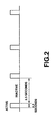
- the mode changeover controller 8 intermittently operates the PWM control circuit 6 so as to turn on the switching element 5 at a given repetition interval and for a given time period.
- This repetition interval is shorter than a time for decreasing an output voltage from the rectifying and smoothing circuit 20 down to a guaranteed load operating voltage due to power consumption of the load and the rectifying and smoothing circuit 20 in the standby mode and is longer than a time for entering a sonic frequency band.
- the time period is longer than a time for stabilizing an output from the DC output means and is longer than a time for entering a sonic frequency band.
- the photo-couplers 11 and 12 are signal couplers for returning a signal from the secondary side to the primary side. These couplers are low power-consuming, normally closed photo-couplers using optical MOS devices for saving currents on standby.
- the AC rectifier 3 is supplied with an AC current from the commercial power input terminal 1 via the AC input filter 2.
- the AC rectifier 3 outputs a DC power by rectifying and smoothing the supplied AC power.
- the DC power activates the startup circuit 4 to supply an activation signal to the PWM control circuit 6.
- the PWM control circuit 6 starts oscillation at a frequency of approximately 100 kHz.
- An oscillation output from the PWM control circuit 6 allows the switching element 5 to perform a switching operation.
- the switching element 5 switches a DC current supplied from the AC rectifier 3 to the primary coil 10A of the converter transformer 10.
- the converter transformer 10 generates a secondary output and a ternary output at the secondary coil 10B and the ternary coil 10C, respectively.
- the ternary output generated at the converter transformer 10's ternary coil 10C is used as a drive power for the PWM control circuit 6 and the mode changeover controller 8.
- the secondary output generated at the converter transformer 10's secondary coil 10B is rectified and smoothed in the rectifying and smoothing circuit 20. This output is used as a drive power for the secondary voltage controller 24 and the mode changeover control signal generator 26. The secondary output is supplied to the load circuit 30 via the current detection resistor 25.
- the secondary voltage controller 24 detects a DC output voltage rectified and smoothed by the rectifying and smoothing circuit 20 via the voltage detection resistor 23. The secondary voltage controller 24 compares this DC output voltage with the reference voltage to obtain an error voltage. The secondary voltage controller 24 returns a control output corresponding to this error voltage to the PWM control circuit 6 via the photo-coupler 11.
- the PWM control circuit 6 PWM-controls switching operations of the switching element 5 by varying oscillation output pulse widths according to the control output, namely the error voltage returned from the secondary voltage controller 24.
- This switching power-supply unit operates in the normal operation mode as mentioned above.
- the mode changeover control signal generator 26 detects via the current detection resistor 25 that a current to the load circuit 30, namely a load consumption current, falls below a specified value, say, 2 mA.
- the mode changeover control signal generator 26 is supplied with a standby signal via the standby signal input terminal 27. In these cases, the mode changeover control signal generator 26 supplies the mode changeover controller 8 via the photo-coupler 12 with a mode changeover control signal for enabling the standby mode.
- the mode changeover controller 8 makes preparations for switching from the normal operation mode to the standby mode.
- the mode changeover control signal is supplied for a specified time, say, 2 seconds, the mode changeover controller 8 controls to change the normal operation mode to the standby mode.
- the mode changeover controller 8 supplies a standby signal indicating the standby mode to the startup circuit 4 and the PWM control circuit 6, then stops the startup circuit 4 to place the PWM control circuit 6 into a standby state.
- the mode changeover control signal generator 26 checks if a current supplied to the load circuit 30. namely a load consumption current increases. Alternatively, the mode changeover control signal generator 26 checks if a standby signal supplied via the standby signal input terminal 27 is released. The mode changeover control signal generator 26 makes these checks through the intermediation of the current detection resistor 25. When a change occurs, the mode changeover control signal generator 26 supplies a mode changeover control signal enabling the normal operation mode to the mode changeover controller 8 via the photo-coupler 12.
- the mode changeover controller 8 controls operation modes using interrupt processing. Namely, when receiving an interrupt by a mode changeover control signal for enabling the normal operation mode, the mode changeover controller 8 immediately supplies the startup circuit 4 and the PWM control circuit 6 with a wakeup signal for enabling the normal operation mode. The mode changeover controller 8 then restores operations of the startup circuit 4 and the PWM control circuit 6 to the normal operation mode.
- an inactive state may continue for a specified period, say, 2.5 seconds or more to apply no interrupt to a mode changeover control signal for enabling the normal operation mode.
- the mode changeover controller 8 forcibly supplies a wakeup signal to the startup circuit 4 and the PWM control circuit 6 for, say, 0.2 seconds to operate these circuits for stabilizing a secondary output voltage.
- various signals such as an increased load current, a signal from the set, and the like.
- this switching power-supply unit operates as a PWM-controlled switching regulator by using a basic oscillation frequency at approximately 100 kHz as the first frequency.
- the switching power-supply unit performs a switching operation with the fixed ON duty at the second frequency which is fixed to a very longer cycle than for the first frequency. This minimizes power consumption in the standby mode.
- the second frequency in this example uses the frequency of 0.37 Hz and the ON duty of 7.5%.
- the second frequency and the ON duty depend on the relationship between an available amount of energy stored in the primary capacitor and a time capable of maintaining a secondary output voltage using that amount of energy.
- the average power consumption is 59 mW.
- the power consumption in the standby mode becomes approximately half or less of that for the 264 V AC input.
- a switching frequency in the standby mode is extremely low at 0.37 Hz. This is outside the sonic frequency band and does not generate a grating noise.
- the frequency and the ON duty are determined as follows, assuming that an input capacity is 47 ⁇ F/400V; a secondary output capacitor size is 1,200 ⁇ F/16V; and a control power capacity is 1,000 ⁇ F/35V.
- This example uses 2.5 seconds with an allowance.
- An effective power in operation is 360 mW. Even if a power supply is soft-started, a power output becomes stable within approximately 10 ms. Thereafter, PWM control is performed to stabilize the secondary output voltage. This operation time can be just 10 ms or more.
- the mode changeover controller 8 using the one-chip microcomputer performs the following steps at the operation startup: setting the CPU environment (step S1), setting the watchdog timer (WDT) (step S2), setting an interrupt (step S3), setting an input/output port (step S4), and pulling up input (step S5).
- a header file is used to set the WDT to 2.5 seconds.
- a port B0 is set to output (step S6).
- a port B1 is set to input (step S7).
- the port B0 output is then turned on (step S8) to activate the startup circuit 4 and the PWM control circuit 6.
- the mode changeover controller waits (step S9) until expiration of a time (0.2 seconds) for forcibly operating the PWM control circuit 6.
- the port B1 is prevented against input chattering (step S10).
- the chattering prevention processing accepts this input at the port B1 as an effective input (new STB). Effective inputs may be decided by majority.
- step S11 results in NO
- the normal operation mode takes effect.
- the port B0 output is turned on (step S12) to restart the WDT (step S13). Control then returns to step S6 and repeats processing from steps S6 to S13.
- step S11 results in YES
- the standby mode takes effect.
- the port B0 output is turned off (step S14) to restart the WDT (step S15).
- the mode changeover controller waits in the sleep mode (step S16). After 2.5 seconds, control returns to step S6 and repeats processing from steps S6 to S16.
- This switching power-supply unit uses the mode changeover controller 8 based on the programmable one-chip microcomputer. By modifying the program software, it is possible to freely set control times and provide a general-purpose power supply. If a program executes erratically, a soft reset is performed using the WDT. The switching power-supply unit resumes automatically.
Landscapes
- Engineering & Computer Science (AREA)
- Power Engineering (AREA)
- Dc-Dc Converters (AREA)
Abstract
Description
Claims (3)
- A switching power-supply unit having a rectifier circuit for converting an alternating current from an alternating power supply to a direct current, a switching element for switching a current rectified by this rectifier circuit, and a primary coil for supplying a current to be switched by this switching element, comprising:a transformer having a secondary coil for inducing power corresponding to current supplied to this primary coil;DC output means for rectifying and smoothing a power induced at this transformer's secondary coil to output a secondary direct current power;switching control means for controlling a switching operation of said switching element so as to output a specified voltage from this DC output means; andcontrol means for controlling operations of said switching control means,wherein said control means, in the normal operation mode, continuously operates said switching control means so as to operate said switching element at a basic oscillation frequency, wherein said control means, in the standby mode, intermittently operates said switching control means so as to turn on said switching element at a given repetition interval and for a given time period, wherein that repetition interval is shorter than a time for decreasing an output voltage from said DC output means down to a guaranteed load operating voltage due to power consumption of the load and said DC output means in the standby mode and is longer than a time for entering a sonic frequency band, and wherein that time period is longer than a time for stabilizing an output from said DC output means and is longer than a time for entering a sonic frequency band.
- The switching power-supply unit according to claim 1. further comprising current detection means for detecting that a load current becomes below a specified value.
wherein said control means performs a control operation for a standby mode when said current detection means detects a load current below a specified value for a specified period in a normal operation mode. - The switching power-supply unit according to claim 1, wherein said control means comprises said microcomputer and uses program software to variably set a control time such as a repetition interval in said standby mode.
Applications Claiming Priority (2)
| Application Number | Priority Date | Filing Date | Title |
|---|---|---|---|
| JP2000027414A JP2001218461A (en) | 2000-01-31 | 2000-01-31 | Switching power supply |
| JP2000027414 | 2000-01-31 |
Publications (3)
| Publication Number | Publication Date |
|---|---|
| EP1122874A2 true EP1122874A2 (en) | 2001-08-08 |
| EP1122874A3 EP1122874A3 (en) | 2004-01-21 |
| EP1122874B1 EP1122874B1 (en) | 2006-11-15 |
Family
ID=18552986
Family Applications (1)
| Application Number | Title | Priority Date | Filing Date |
|---|---|---|---|
| EP01300573A Expired - Lifetime EP1122874B1 (en) | 2000-01-31 | 2001-01-23 | Switching power-supply units |
Country Status (7)
| Country | Link |
|---|---|
| US (1) | US6549429B2 (en) |
| EP (1) | EP1122874B1 (en) |
| JP (1) | JP2001218461A (en) |
| KR (1) | KR100746843B1 (en) |
| CN (1) | CN1177403C (en) |
| DE (1) | DE60124436T2 (en) |
| TW (1) | TW512580B (en) |
Cited By (3)
| Publication number | Priority date | Publication date | Assignee | Title |
|---|---|---|---|---|
| DE102005044723A1 (en) * | 2005-09-19 | 2007-03-22 | Endress + Hauser Flowtec Ag | Switching power supply for operating e.g. measuring devices, has watch dog circuit arranged on secondary side of switching unit, and monitoring switching activity of switching units |
| WO2012094483A3 (en) * | 2011-01-07 | 2013-03-21 | Ysi Incorporated | Switch-mode power supply with isolation transformer and standby mode |
| EP3065507A1 (en) * | 2015-03-03 | 2016-09-07 | Helvar Oy Ab | Method and apparatus for controlling a primary stage of a light driver device |
Families Citing this family (56)
| Publication number | Priority date | Publication date | Assignee | Title |
|---|---|---|---|---|
| JP3578124B2 (en) * | 2001-08-31 | 2004-10-20 | ソニー株式会社 | Switching power supply |
| JP2004088959A (en) * | 2002-08-28 | 2004-03-18 | Sharp Corp | Switching power supply |
| KR100484160B1 (en) * | 2002-09-06 | 2005-04-19 | 삼성전자주식회사 | Apparatus for measuring consumption power |
| JP3954481B2 (en) * | 2002-11-29 | 2007-08-08 | ローム株式会社 | DC-AC converter and its controller IC |
| US7492620B2 (en) * | 2002-11-29 | 2009-02-17 | Rohm Co., Ltd. | DC-AC converter and controller IC thereof |
| DE10330605A1 (en) * | 2003-07-07 | 2005-01-27 | Deutsche Thomson-Brandt Gmbh | Switching Power Supply |
| US7019995B2 (en) * | 2003-11-15 | 2006-03-28 | Hewlett-Packard Development Company, L.P. | Power supply having reduced-power mode |
| KR101020243B1 (en) * | 2004-06-16 | 2011-03-07 | 페어차일드코리아반도체 주식회사 | Switching-mode power supplies |
| JP2006050760A (en) * | 2004-08-04 | 2006-02-16 | New Japan Radio Co Ltd | Switching power supply circuit and control method therefor |
| US7542257B2 (en) * | 2004-09-10 | 2009-06-02 | Philips Solid-State Lighting Solutions, Inc. | Power control methods and apparatus for variable loads |
| JP4536467B2 (en) * | 2004-09-17 | 2010-09-01 | 株式会社エヌ・ティ・ティ・ドコモ | Flat circuit housing |
| JP4578198B2 (en) * | 2004-09-30 | 2010-11-10 | 株式会社リコー | Switching regulator |
| JP2006129687A (en) * | 2004-10-01 | 2006-05-18 | Nec Tokin Corp | Ac adapter |
| US6995989B1 (en) * | 2004-10-20 | 2006-02-07 | Niko Semiconductor Co., Ltd. | Half-bridge-type control signal generating circuit and method thereof |
| TWI255985B (en) * | 2004-12-06 | 2006-06-01 | Benq Corp | A standby mode power saving electronic apparatus, power supply and method of powering the standby mode power saving electronic apparatus |
| US7596367B2 (en) * | 2005-02-09 | 2009-09-29 | Sony Corporation | System and method for standby mode in directional signal receiver |
| CN100433520C (en) * | 2005-03-04 | 2008-11-12 | 崇贸科技股份有限公司 | Switching type control device for primary side control output current of power supply |
| JP4212569B2 (en) | 2005-04-01 | 2009-01-21 | 株式会社デンソー | Switching device |
| JP4498967B2 (en) | 2005-04-01 | 2010-07-07 | 株式会社日本自動車部品総合研究所 | Switching device |
| JP4578303B2 (en) | 2005-04-01 | 2010-11-10 | 株式会社日本自動車部品総合研究所 | Switching device |
| KR100710086B1 (en) * | 2005-08-22 | 2007-04-20 | 한국전기연구원 | Switch mode power supply and its power consumption reduction method |
| US20070085574A1 (en) * | 2005-10-11 | 2007-04-19 | Atron Lo | Audio signal detection utilizing low power standby power supply |
| JP4844151B2 (en) * | 2006-02-10 | 2011-12-28 | サンケン電気株式会社 | Switching power supply |
| JP5167705B2 (en) * | 2007-07-02 | 2013-03-21 | 富士電機株式会社 | Switching power supply |
| US8903577B2 (en) | 2009-10-30 | 2014-12-02 | Lsi Industries, Inc. | Traction system for electrically powered vehicles |
| US7598683B1 (en) | 2007-07-31 | 2009-10-06 | Lsi Industries, Inc. | Control of light intensity using pulses of a fixed duration and frequency |
| US8604709B2 (en) | 2007-07-31 | 2013-12-10 | Lsi Industries, Inc. | Methods and systems for controlling electrical power to DC loads |
| KR100920956B1 (en) * | 2007-10-18 | 2009-10-09 | 엘지이노텍 주식회사 | Power supply |
| JP5561916B2 (en) * | 2008-07-11 | 2014-07-30 | ミツミ電機株式会社 | Battery status monitoring device |
| TWI382302B (en) * | 2008-07-18 | 2013-01-11 | Hon Hai Prec Ind Co Ltd | Power supply circuit for pwm controller |
| WO2010036202A1 (en) * | 2008-09-23 | 2010-04-01 | Stl Energy Technology (S) Pte Ltd | Battery pack and method of battery pack power management |
| TWI390818B (en) * | 2009-07-14 | 2013-03-21 | Richpower Microelectronics | Apparatus and method for improving the standby efficiency of a charger, and ultra low standby power charge |
| TWI398764B (en) * | 2009-07-21 | 2013-06-11 | Richpower Microelectronics | Apparatus and method for reducing the standby power consumption of a display, and display with low standby power consumption |
| CN102983750B (en) * | 2009-07-23 | 2015-03-04 | 台达电子工业股份有限公司 | Switching power conversion circuit and its applicable power supply |
| CN101964599B (en) * | 2009-07-23 | 2013-04-17 | 台达电子工业股份有限公司 | Switching power conversion circuit and its applicable power supply |
| CN102142773A (en) * | 2010-02-03 | 2011-08-03 | 通嘉科技股份有限公司 | Power management integrated circuit and power management method |
| KR20130061678A (en) | 2010-04-16 | 2013-06-11 | 가부시키가이샤 한도오따이 에네루기 켄큐쇼 | Power source circuit |
| US9331565B2 (en) | 2010-07-14 | 2016-05-03 | Delta Electronics (Shanghai) Co., Ltd. | Switching power conversion circuit and power supply using same |
| US8704504B2 (en) | 2010-09-03 | 2014-04-22 | Semiconductor Energy Laboratory Co., Ltd. | Power supply circuit comprising detection circuit including reference voltage circuits as reference voltage generation circuits |
| US8953341B2 (en) * | 2011-05-09 | 2015-02-10 | Infineon Technologies Ag | Converter with reduced power consumption |
| JP5660575B2 (en) * | 2011-07-08 | 2015-01-28 | 新電元工業株式会社 | Control circuit and switching power supply |
| US9461546B2 (en) * | 2013-02-08 | 2016-10-04 | Advanced Charging Technologies, LLC | Power device and method for delivering power to electronic devices |
| JP6460592B2 (en) | 2013-07-31 | 2019-01-30 | 株式会社半導体エネルギー研究所 | DC-DC converter and semiconductor device |
| KR102151935B1 (en) * | 2013-11-12 | 2020-09-04 | 삼성전자주식회사 | Electronic apparatus and power controlling method thereof |
| US20160056724A1 (en) * | 2014-08-21 | 2016-02-25 | Texas Instruments Incorporated | Switching Power Supplies And Methods Of Operating Switching Power Supplies |
| TWI556563B (en) | 2014-09-12 | 2016-11-01 | Alpha & Omega Semiconductor Cayman Ltd | Fixed on-time switching type switching device |
| TWI581555B (en) | 2014-09-12 | 2017-05-01 | Alpha And Omega Semiconductor (Cayman) Ltd | Fixed on-time switching converter |
| TWI549412B (en) | 2014-09-12 | 2016-09-11 | Alpha & Omega Semiconductor Cayman Ltd | Fixed on-time switching type switching device |
| TWI565211B (en) | 2014-09-12 | 2017-01-01 | Alpha And Omega Semiconductor (Cayman) Ltd | Constant on-time switching converter |
| US20170117813A1 (en) * | 2015-10-21 | 2017-04-27 | Quanta Computer Inc. | Method and system for testing a power supply unit |
| JP6700772B2 (en) * | 2015-12-18 | 2020-05-27 | キヤノン株式会社 | Power supply device and image forming apparatus |
| US10326371B2 (en) | 2017-08-23 | 2019-06-18 | Semiconductor Components Industries, Llc | Providing adaptive output power |
| US10320301B2 (en) * | 2017-09-15 | 2019-06-11 | Semiconductor Components Industries, Llc | Power converter responsive to device connection status |
| US11211874B2 (en) * | 2019-02-08 | 2021-12-28 | Dialog Semiconductor (Uk) Limited | Flyback converter with no-load power control for reduced power consumption |
| CN110855279A (en) * | 2019-12-11 | 2020-02-28 | 贵州航天凯山石油仪器有限公司 | A circuit breaker for regularly cutting off the power supply |
| US20240334569A1 (en) * | 2023-03-29 | 2024-10-03 | ERP Power, LLC | Lighting system including a fast low-power startup circuit |
Family Cites Families (14)
| Publication number | Priority date | Publication date | Assignee | Title |
|---|---|---|---|---|
| DE3731644A1 (en) * | 1987-09-19 | 1989-03-30 | Thomson Brandt Gmbh | CIRCUIT ARRANGEMENT FOR A REGULATED SWITCHING POWER SUPPLY |
| US4937728A (en) * | 1989-03-07 | 1990-06-26 | Rca Licensing Corporation | Switch-mode power supply with burst mode standby operation |
| US5119284A (en) * | 1990-04-05 | 1992-06-02 | General Electric Company | Efficient power supply post regulation |
| DE4212472B4 (en) * | 1992-04-14 | 2006-02-09 | Deutsche Thomson-Brandt Gmbh | Free-running switching power supply |
| DE19518863A1 (en) * | 1995-05-23 | 1996-11-28 | Thomson Brandt Gmbh | Switching power supply with standby mode |
| US5764495A (en) * | 1996-05-01 | 1998-06-09 | Compaq Computer Corporation | Variable-frequency variable-input-voltage converter with minimum frequency limit |
| JPH1023354A (en) * | 1996-06-29 | 1998-01-23 | Matsushita Electric Ind Co Ltd | Power supply for television receiver |
| US5956240A (en) * | 1996-11-15 | 1999-09-21 | Thomson Consumer Electronics, Inc. | Quick-reset circuit for auxiliary power supply |
| US6104622A (en) * | 1997-04-30 | 2000-08-15 | Fidelix Y.K. | Power supply apparatus for reduction of power consumption |
| US6005377A (en) * | 1997-09-17 | 1999-12-21 | Lucent Technologies Inc. | Programmable digital controller for switch mode power conversion and power supply employing the same |
| JP2000116027A (en) * | 1998-03-10 | 2000-04-21 | Fiderikkusu:Kk | Power supply device |
| JP3497075B2 (en) * | 1998-03-20 | 2004-02-16 | シャープ株式会社 | Switching power supply circuit |
| DE19826152A1 (en) * | 1998-06-12 | 1999-12-16 | Thomson Brandt Gmbh | Arrangement with a switching power supply and a microprocessor |
| US6018467A (en) * | 1999-07-28 | 2000-01-25 | Philips Electronics North America Corporation | Resonant mode power supply having an efficient low power stand-by mode |
-
2000
- 2000-01-31 JP JP2000027414A patent/JP2001218461A/en not_active Withdrawn
-
2001
- 2001-01-23 DE DE60124436T patent/DE60124436T2/en not_active Expired - Fee Related
- 2001-01-23 EP EP01300573A patent/EP1122874B1/en not_active Expired - Lifetime
- 2001-01-29 TW TW090101655A patent/TW512580B/en not_active IP Right Cessation
- 2001-01-30 KR KR1020010004254A patent/KR100746843B1/en not_active Expired - Fee Related
- 2001-01-31 US US09/774,898 patent/US6549429B2/en not_active Expired - Fee Related
- 2001-01-31 CN CNB011017511A patent/CN1177403C/en not_active Expired - Fee Related
Cited By (3)
| Publication number | Priority date | Publication date | Assignee | Title |
|---|---|---|---|---|
| DE102005044723A1 (en) * | 2005-09-19 | 2007-03-22 | Endress + Hauser Flowtec Ag | Switching power supply for operating e.g. measuring devices, has watch dog circuit arranged on secondary side of switching unit, and monitoring switching activity of switching units |
| WO2012094483A3 (en) * | 2011-01-07 | 2013-03-21 | Ysi Incorporated | Switch-mode power supply with isolation transformer and standby mode |
| EP3065507A1 (en) * | 2015-03-03 | 2016-09-07 | Helvar Oy Ab | Method and apparatus for controlling a primary stage of a light driver device |
Also Published As
| Publication number | Publication date |
|---|---|
| DE60124436T2 (en) | 2007-09-27 |
| EP1122874A3 (en) | 2004-01-21 |
| US20010010638A1 (en) | 2001-08-02 |
| CN1177403C (en) | 2004-11-24 |
| JP2001218461A (en) | 2001-08-10 |
| KR100746843B1 (en) | 2007-08-09 |
| KR20010078158A (en) | 2001-08-20 |
| EP1122874B1 (en) | 2006-11-15 |
| TW512580B (en) | 2002-12-01 |
| US6549429B2 (en) | 2003-04-15 |
| DE60124436D1 (en) | 2006-12-28 |
| CN1319940A (en) | 2001-10-31 |
Similar Documents
| Publication | Publication Date | Title |
|---|---|---|
| EP1122874B1 (en) | Switching power-supply units | |
| US6608471B2 (en) | Off-line converter with digital control | |
| US5359281A (en) | Quick-start and overvoltage protection for a switching regulator circuit | |
| JP3652351B2 (en) | Switching power supply | |
| KR100273439B1 (en) | Apparatus and method for reducing power consumption of a power supply | |
| US20050041360A1 (en) | Systems and methods for achieving low power standby through interaction between a microcontroller and a switching mode power supply | |
| US20090256534A1 (en) | Power supply control method and apparatus | |
| JP2009159727A (en) | Converter power supply circuit and converter power supply driving method | |
| JP3697218B2 (en) | Power supply | |
| JP3425403B2 (en) | Semiconductor device and switching power supply device using this semiconductor device | |
| JPH07143741A (en) | Switching power supply | |
| JPH07170729A (en) | Switching power supply | |
| JP2004120826A (en) | Switching power supply, image forming apparatus, and method for reducing power consumption | |
| JP2001045749A (en) | Switching power supply device and operation method thereof | |
| JP3415566B2 (en) | Switching power supply | |
| JP4834930B2 (en) | Method and apparatus for controlling DC / DC converter | |
| JP3422324B2 (en) | Switching power supply | |
| JP2002315319A (en) | Switching power supply | |
| JP4720013B2 (en) | Electronic electrical equipment | |
| JP4006910B2 (en) | Power supply | |
| JP2000324817A (en) | Power supply circuit | |
| JPH10337019A (en) | Switching power supply | |
| JP2682406B2 (en) | Constant voltage power supply | |
| JP2002199613A (en) | Rechargeable battery charging circuit | |
| JPH11168884A (en) | Dc power supply circuit |
Legal Events
| Date | Code | Title | Description |
|---|---|---|---|
| PUAI | Public reference made under article 153(3) epc to a published international application that has entered the european phase |
Free format text: ORIGINAL CODE: 0009012 |
|
| AK | Designated contracting states |
Kind code of ref document: A2 Designated state(s): AT BE CH CY DE DK ES FI FR GB GR IE IT LI LU MC NL PT SE TR |
|
| AX | Request for extension of the european patent |
Free format text: AL;LT;LV;MK;RO;SI |
|
| PUAL | Search report despatched |
Free format text: ORIGINAL CODE: 0009013 |
|
| AK | Designated contracting states |
Kind code of ref document: A3 Designated state(s): AT BE CH CY DE DK ES FI FR GB GR IE IT LI LU MC NL PT SE TR |
|
| AX | Request for extension of the european patent |
Extension state: AL LT LV MK RO SI |
|
| 17P | Request for examination filed |
Effective date: 20040705 |
|
| AKX | Designation fees paid |
Designated state(s): DE GB |
|
| 17Q | First examination report despatched |
Effective date: 20050404 |
|
| GRAP | Despatch of communication of intention to grant a patent |
Free format text: ORIGINAL CODE: EPIDOSNIGR1 |
|
| GRAS | Grant fee paid |
Free format text: ORIGINAL CODE: EPIDOSNIGR3 |
|
| GRAA | (expected) grant |
Free format text: ORIGINAL CODE: 0009210 |
|
| AK | Designated contracting states |
Kind code of ref document: B1 Designated state(s): DE GB |
|
| REG | Reference to a national code |
Ref country code: GB Ref legal event code: FG4D |
|
| REF | Corresponds to: |
Ref document number: 60124436 Country of ref document: DE Date of ref document: 20061228 Kind code of ref document: P |
|
| PGFP | Annual fee paid to national office [announced via postgrant information from national office to epo] |
Ref country code: GB Payment date: 20070117 Year of fee payment: 7 |
|
| PGFP | Annual fee paid to national office [announced via postgrant information from national office to epo] |
Ref country code: DE Payment date: 20070118 Year of fee payment: 7 |
|
| PLBE | No opposition filed within time limit |
Free format text: ORIGINAL CODE: 0009261 |
|
| STAA | Information on the status of an ep patent application or granted ep patent |
Free format text: STATUS: NO OPPOSITION FILED WITHIN TIME LIMIT |
|
| 26N | No opposition filed |
Effective date: 20070817 |
|
| GBPC | Gb: european patent ceased through non-payment of renewal fee |
Effective date: 20080123 |
|
| PG25 | Lapsed in a contracting state [announced via postgrant information from national office to epo] |
Ref country code: DE Free format text: LAPSE BECAUSE OF NON-PAYMENT OF DUE FEES Effective date: 20080801 |
|
| PG25 | Lapsed in a contracting state [announced via postgrant information from national office to epo] |
Ref country code: GB Free format text: LAPSE BECAUSE OF NON-PAYMENT OF DUE FEES Effective date: 20080123 |