EP1122815A2 - An antenna for a handset - Google Patents
An antenna for a handset Download PDFInfo
- Publication number
- EP1122815A2 EP1122815A2 EP01300548A EP01300548A EP1122815A2 EP 1122815 A2 EP1122815 A2 EP 1122815A2 EP 01300548 A EP01300548 A EP 01300548A EP 01300548 A EP01300548 A EP 01300548A EP 1122815 A2 EP1122815 A2 EP 1122815A2
- Authority
- EP
- European Patent Office
- Prior art keywords
- antenna device
- branches
- conducting layer
- antenna
- frequency bands
- Prior art date
- Legal status (The legal status is an assumption and is not a legal conclusion. Google has not performed a legal analysis and makes no representation as to the accuracy of the status listed.)
- Ceased
Links
- 230000008878 coupling Effects 0.000 claims description 10
- 238000010168 coupling process Methods 0.000 claims description 10
- 238000005859 coupling reaction Methods 0.000 claims description 10
- 238000001746 injection moulding Methods 0.000 claims 1
- 230000009977 dual effect Effects 0.000 description 5
- ZMHWQAHZKUPENF-UHFFFAOYSA-N 1,2-dichloro-3-(4-chlorophenyl)benzene Chemical compound C1=CC(Cl)=CC=C1C1=CC=CC(Cl)=C1Cl ZMHWQAHZKUPENF-UHFFFAOYSA-N 0.000 description 3
- 230000001413 cellular effect Effects 0.000 description 2
- 230000005684 electric field Effects 0.000 description 2
- 230000001939 inductive effect Effects 0.000 description 2
- 238000006073 displacement reaction Methods 0.000 description 1
- 230000000694 effects Effects 0.000 description 1
- 230000005672 electromagnetic field Effects 0.000 description 1
- 230000013011 mating Effects 0.000 description 1
- 230000002093 peripheral effect Effects 0.000 description 1
Images


Classifications
-
- H—ELECTRICITY
- H01—ELECTRIC ELEMENTS
- H01Q—ANTENNAS, i.e. RADIO AERIALS
- H01Q21/00—Antenna arrays or systems
- H01Q21/30—Combinations of separate antenna units operating in different wavebands and connected to a common feeder system
-
- H—ELECTRICITY
- H01—ELECTRIC ELEMENTS
- H01Q—ANTENNAS, i.e. RADIO AERIALS
- H01Q1/00—Details of, or arrangements associated with, antennas
- H01Q1/12—Supports; Mounting means
- H01Q1/22—Supports; Mounting means by structural association with other equipment or articles
- H01Q1/24—Supports; Mounting means by structural association with other equipment or articles with receiving set
- H01Q1/241—Supports; Mounting means by structural association with other equipment or articles with receiving set used in mobile communications, e.g. GSM
- H01Q1/242—Supports; Mounting means by structural association with other equipment or articles with receiving set used in mobile communications, e.g. GSM specially adapted for hand-held use
- H01Q1/243—Supports; Mounting means by structural association with other equipment or articles with receiving set used in mobile communications, e.g. GSM specially adapted for hand-held use with built-in antennas
-
- H—ELECTRICITY
- H01—ELECTRIC ELEMENTS
- H01Q—ANTENNAS, i.e. RADIO AERIALS
- H01Q1/00—Details of, or arrangements associated with, antennas
- H01Q1/36—Structural form of radiating elements, e.g. cone, spiral, umbrella; Particular materials used therewith
- H01Q1/38—Structural form of radiating elements, e.g. cone, spiral, umbrella; Particular materials used therewith formed by a conductive layer on an insulating support
-
- H—ELECTRICITY
- H01—ELECTRIC ELEMENTS
- H01Q—ANTENNAS, i.e. RADIO AERIALS
- H01Q5/00—Arrangements for simultaneous operation of antennas on two or more different wavebands, e.g. dual-band or multi-band arrangements
- H01Q5/30—Arrangements for providing operation on different wavebands
- H01Q5/307—Individual or coupled radiating elements, each element being fed in an unspecified way
- H01Q5/342—Individual or coupled radiating elements, each element being fed in an unspecified way for different propagation modes
- H01Q5/357—Individual or coupled radiating elements, each element being fed in an unspecified way for different propagation modes using a single feed point
- H01Q5/364—Creating multiple current paths
- H01Q5/371—Branching current paths
-
- H—ELECTRICITY
- H01—ELECTRIC ELEMENTS
- H01Q—ANTENNAS, i.e. RADIO AERIALS
- H01Q9/00—Electrically-short antennas having dimensions not more than twice the operating wavelength and consisting of conductive active radiating elements
- H01Q9/04—Resonant antennas
- H01Q9/0407—Substantially flat resonant element parallel to ground plane, e.g. patch antenna
- H01Q9/0442—Substantially flat resonant element parallel to ground plane, e.g. patch antenna with particular tuning means
Definitions
- the invention relates to a dual band antenna for a handset.
- Such an antenna includes a metallic plate or layer acting as ground plane for the antenna, a resonator plate or layer acting as radiating element(s), and a feeding point supplying the signal to the antenna.
- This phone has a dielectric antenna body covered by a metallic pattern forming two radiating elements - one for each band.
- the dielectric antenna body is inside the phone snapped onto a metallic shield acting as resonator plane.
- the antenna used in Nokia 3210TM is a PIFA (Planar Inverted F-Antennas) antenna and is described in GB 9828533.1, GB 9828364.1, and GB 9828535.6 - all filed in December 1998.
- PIFA Planar Inverted F-Antennas
- WO 95/24746 describes a single band internal antenna having a dielectric body coated with a metallic layer on two substantially parallel surfaces.
- US 5.764.190 describes a capacity loaded PIFA according to which an extra plate is interposed in between the ground plane and the radiating element.
- US 5.764.190 describes how to provide a longitudinal slit in the resonator layer in order to obtain two radiating elements. A capacitive feeding concept is used.
- GSM works in the 900 MHz band (uplink: 890-915 MHz (mobile to base-station), and downlink: 935-960 MHz (base-station to mobile)) and in the 1800 MHz band (uplink: 1710-1785 MHz (mobile to base-station), and downlink: 1805-1880 MHz (base-station to mobile)).
- An object of the invention is to provide a dual band antenna having a reduced overall size.
- a dual band antenna device having a first conducting layer acting as resonator plane for the antenna device, a second conducting layer, that is substantial parallell with the first conducting layer, and acting as ground plane, and a dielectric body on which said first conducting layer is provided.
- the first conducting layer comprises two branches, and both branches will contribute to the matching of the antenna device in both hands.
- the full patch area may be used either for radiaing an electromagnetic field or for mating the antenna.
- the first one of said two branches is quarter-wave resonant in a first one of said two bands, and half-wave resonant in a second one of said two bands, while the second one of said two branches provides a resonant matching in said first one of said two bands, and will appear as a quarter-wave resonant stub in said second one of said two bands.
- the two bands wil have center frequencies in approximately 920 MHz and in approximately 1800 MHz, respectively.
- the antenna elements constituted by the branches have been folded in order to reduce the RF coupling between the two branches. This can be done by locating the open ends away from each other, as well as aligning the currents of the two at 90 degrees angle. Hereby the capacitive coupling between the open ends of the stubs (electrical field) will be reduced. Furthermore the inductive coupling between the branches where the currents are strong (close to the feed and at 1800 MHz at the middle of the 900 MHz as well) will be reduced. Locating the feed close to the edge of the PCB will also increase bandwidth.
- the layout distributes the currents in a large area of the patch, which is desirable.
- Fig. 1 and 2 shows a preferred embodiment of a phone according to the invention, and it will be seen that the phone, which is generally designated by 1, comprises a user interface having a keypad 2, a display 3, an on/off button 4, a speaker 5, and a microphone 6 (only openings are shown).
- the phone 1 according to the preferred embodiment is adapted for communication via a cellular network, but could have been designed for a cordless network as well.
- the keypad 2 has a first group 7 of keys as alphanumeric keys, two soft keys 8, two call handling keys 9, and a cursor navigation key 10.
- the present functionality of the soft keys 8 is shown in separate fields in the display 3 just above the keys 8, and the call handling keys 9 are used for establishing a call or a conference call, terminating a call or rejecting an incoming call.
- Fig. 3 schematically shows the most important parts of a preferred embodiment of the phone, said parts being essential to the understanding of the invention.
- the preferred embodiment of the phone of the invention is adapted for use in connection with a GSM 900 MHz and a GSM 1800 MHz network.
- the processor 18 controls the communication with the network via the transmitter/receiver circuit 19 and an internal antenna 20 that will be discussed in details below.
- the microphone 6 transforms the user's speech into analog signals, the analog signals formed thereby are A/D converted in an A/D converter (not shown) before the speech is encoded in an audio part 14.
- the encoded speech signal is transferred to the processor 18, which i.a. supports the GSM terminal software.
- the processor 18 also forms the interface to the peripheral units of the apparatus, including a RAM memory 17a and a Flash ROM memory 17b, a SIM card 16, the display 3 and the keypad 2 (as well as data, power supply, etc.).
- the audio part 14 speech-decodes the signal, which is transferred from the processor 18 to the earpiece 5 via a D/A converter (not shown).
- the antenna is based upon the PIFA principle.
- the patch 24 consists of two branches 25, 26 connected in parallel to the feed of the antenna.
- One branch 26 is quarter-wave resonant at approximately 920 MHz (centre of GSM 900 MHz band)
- the other branch 25 provides a resonant matching at approximately 1800 MHz (centre of 1800 MHz band).
- the 900 MHz branch 26 will basically be half-wave resonant, whereas the 1800 MHz branch 25 will appear as a quarter-wave resonant stub.
- both branches 25, 26 will in both bands contribute to the matching of the antenna 20.
- the patches In order to reduce the size of the antenna without sacrificing bandwidth, the patches have been folded in a specific manner. Bandwidth will benefit from reducing the RF coupling between the two branches25, 26. What is desired is to reduce the capacitive coupling between the open ends 27, 28 of the stubs (electrical field) and reduce the inductive coupling between the branches where the currents are strong (close to the feed 29 and at 1800 MHz at the middle of the 900 MHz as well). This can be done by locating the open ends away from each other, as well as aligning the currents of the two at 90 degrees angle. Locating the feed 29 close to the edge of the PCB will also increase bandwidth.
- the layout distributes the currents in a large area of the patch, which is desirable.
- the two branches 25, 26 will influence each other regarding tuning of the centre frequencies.
- the obvious way of tuning the antenna is to increase/decrease the length of the branches, but this will not provide optimum tuning since they both affect the 900 MHz as well as the 1800MHz frequencies.
- capacitive coupling between the two branches as well as between the first part and the end 28 of the 900 MHz branch 26 has been used.
- the inductance along the length of the patches has been carefully tuned for achieving best bandwidth as well as centering both bands of operation.
- the feeding of the patch consists of two strips 29, 30 - one of these strips 29 is connected to the RF feed provided on the PCB 22 via a not shown standard spring connector, and the other strip 30 is connected to ground of the PCB 22, and a screw 21 is used for ensuring a sufficient mechanical pressure.
- the strips 29, 30 have been located close together in order to reduce the Q-value of the antenna 20 and hence increase the bandwidth of the antenna. Also this arrangement provides better flexibility for the patch layout since the feed occupies less area on the patch.
- the antenna 20 is provided with guide pins 30 to prevent the antenna 20 against a displacement relative to the PCB 22. It has been verified that the antenna as claimed fulfills the requirements for type approval for a GSM 900/1800 MHz phone. This means that the antenna provides a sufficient gain in both frequency bands.
- the overall width W of the antenna is 36 mm, the length L of the antenna is 19 mm and the height H is 9 mm.
Landscapes
- Engineering & Computer Science (AREA)
- Computer Networks & Wireless Communication (AREA)
- Waveguide Aerials (AREA)
- Support Of Aerials (AREA)
Abstract
Description
- The invention relates to a dual band antenna for a handset. Such an antenna includes a metallic plate or layer acting as ground plane for the antenna, a resonator plate or layer acting as radiating element(s), and a feeding point supplying the signal to the antenna.
- The applicant launched recently a new GSM dual band phone named Nokia 3210™. This phone has a dielectric antenna body covered by a metallic pattern forming two radiating elements - one for each band. The dielectric antenna body is inside the phone snapped onto a metallic shield acting as resonator plane. The antenna used in Nokia 3210™ is a PIFA (Planar Inverted F-Antennas) antenna and is described in GB 9828533.1, GB 9828364.1, and GB 9828535.6 - all filed in December 1998.
- WO 95/24746 describes a single band internal antenna having a dielectric body coated with a metallic layer on two substantially parallel surfaces.
- US 5.764.190 describes a capacity loaded PIFA according to which an extra plate is interposed in between the ground plane and the radiating element.
- US 5.764.190 describes how to provide a longitudinal slit in the resonator layer in order to obtain two radiating elements. A capacitive feeding concept is used.
- A letter by Z. D. Lui and P. S. Hall, "Dual-Frequency Planar Inverted-F Antenna", is published in IEEE Transactions on Antennas and Propagation, October 1997, Volume 45,
Number 10. This letter describes a number of solutions - one of these having a rectangular patch for the 900 MHz band. This patch is provided with an L-shaped slot separating one quarter of the 900 MHz band for acting as resonating element in 1800 MHz band. - GSM works in the 900 MHz band (uplink: 890-915 MHz (mobile to base-station), and downlink: 935-960 MHz (base-station to mobile)) and in the 1800 MHz band (uplink: 1710-1785 MHz (mobile to base-station), and downlink: 1805-1880 MHz (base-station to mobile)).
- An object of the invention is to provide a dual band antenna having a reduced overall size.
- This object is achieved by a dual band antenna device having a first conducting layer acting as resonator plane for the antenna device, a second conducting layer, that is substantial parallell with the first conducting layer, and acting as ground plane, and a dielectric body on which said first conducting layer is provided. The first conducting layer comprises two branches, and both branches will contribute to the matching of the antenna device in both hands. Hereby the full patch area may be used either for radiaing an electromagnetic field or for mating the antenna.
- Preferably the first one of said two branches is quarter-wave resonant in a first one of said two bands, and half-wave resonant in a second one of said two bands, while the second one of said two branches provides a resonant matching in said first one of said two bands, and will appear as a quarter-wave resonant stub in said second one of said two bands. When the antenna device is used in a GSM dual band phone the two bands wil have center frequencies in approximately 920 MHz and in approximately 1800 MHz, respectively.
- By placing the strips of the feeding means in parallel close together the Q-value of the antenna will be reduced and hence the bandwidth of the antenna will be increased. Also this arrangement provides better flexibility for the patch layout since the feed occupies less area on the patch.
- According to the referred embodiment the antenna elements constituted by the branches have been folded in order to reduce the RF coupling between the two branches. This can be done by locating the open ends away from each other, as well as aligning the currents of the two at 90 degrees angle.
Hereby the capacitive coupling between the open ends of the stubs (electrical field) will be reduced. Furthermore the inductive coupling between the branches where the currents are strong (close to the feed and at 1800 MHz at the middle of the 900 MHz as well) will be reduced. Locating the feed close to the edge of the PCB will also increase bandwidth. - Besides minimizing the coupling voltage/voltage and current/current of the two branches, the layout distributes the currents in a large area of the patch, which is desirable.
- For a better understanding of the present invention and to understand how the same may be brought into effect reference will now be made, by way of example only, to accompanying drawings, in which:-
- Fig. 1 and 2 illustrates in perspective a preferred embodiment of a hand portable phone according to the invention seen from the front and rear side, respectively.
- Fig. 3 schematically shows the essential parts of a telephone for communication with a cellular or cordless network.
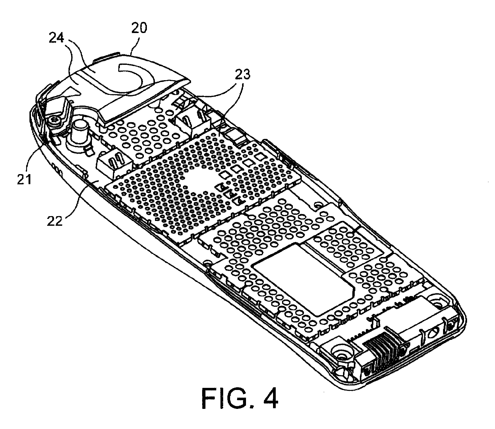
- Fig. 4 shows in perspective view the antenna body mounted onto a metallic inner cover of the phone shown in fig. 1 and 2.
- Fig. 5 and 6 illustrates in perspective details of the antenna body according to the invention seen from the front and rear side, respectively.
-
- Fig. 1 and 2 shows a preferred embodiment of a phone according to the invention, and it will be seen that the phone, which is generally designated by 1, comprises a user interface having a
keypad 2, adisplay 3, an on/off button 4, aspeaker 5, and a microphone 6 (only openings are shown). The phone 1 according to the preferred embodiment is adapted for communication via a cellular network, but could have been designed for a cordless network as well. - According to the preferred embodiment the
keypad 2 has a first group 7 of keys as alphanumeric keys, twosoft keys 8, twocall handling keys 9, and acursor navigation key 10. The present functionality of thesoft keys 8 is shown in separate fields in thedisplay 3 just above thekeys 8, and thecall handling keys 9 are used for establishing a call or a conference call, terminating a call or rejecting an incoming call. - Fig. 3 schematically shows the most important parts of a preferred embodiment of the phone, said parts being essential to the understanding of the invention. The preferred embodiment of the phone of the invention is adapted for use in connection with a GSM 900 MHz and a GSM 1800 MHz network. The
processor 18 controls the communication with the network via the transmitter/receiver circuit 19 and aninternal antenna 20 that will be discussed in details below. - The
microphone 6 transforms the user's speech into analog signals, the analog signals formed thereby are A/D converted in an A/D converter (not shown) before the speech is encoded in anaudio part 14. The encoded speech signal is transferred to theprocessor 18, which i.a. supports the GSM terminal software. Theprocessor 18 also forms the interface to the peripheral units of the apparatus, including aRAM memory 17a and aFlash ROM memory 17b, aSIM card 16, thedisplay 3 and the keypad 2 (as well as data, power supply, etc.). Theaudio part 14 speech-decodes the signal, which is transferred from theprocessor 18 to theearpiece 5 via a D/A converter (not shown). - According to the preferred embodiment of the invention the antenna is based upon the PIFA principle. In order to achieve optimum performance at two frequency bands, the GSM 900 MHz band and GSM 1800 MHz band, according to the preferred embodiment shown in fig. 4, 5 and 6, the
patch 24 consists of twobranches 25, 26 connected in parallel to the feed of the antenna. Onebranch 26 is quarter-wave resonant at approximately 920 MHz (centre of GSM 900 MHz band), the other branch 25 provides a resonant matching at approximately 1800 MHz (centre of 1800 MHz band). At 1800 MHz, the 900MHz branch 26 will basically be half-wave resonant, whereas the 1800 MHz branch 25 will appear as a quarter-wave resonant stub. However, bothbranches 25, 26 will in both bands contribute to the matching of theantenna 20. - In fig. 4 the rear cover of the phone shown in fig. 1 and 2 has been removed in order to expose the internal parts of the phone. It is seen how the
antenna 20 is fixed to a PrintedCircuit Board 22 of the phone by means of ascrew 21. Theantenna 20 is coated withmetallic patches 24 constituting the radiating antenna elements, whilemetallic shielding cans 23 provides the ground plane of the PIFA antenna. - In order to reduce the size of the antenna without sacrificing bandwidth, the patches have been folded in a specific manner. Bandwidth will benefit from reducing the RF coupling between the two branches25, 26. What is desired is to reduce the capacitive coupling between the
open ends feed 29 and at 1800 MHz at the middle of the 900 MHz as well). This can be done by locating the open ends away from each other, as well as aligning the currents of the two at 90 degrees angle. Locating thefeed 29 close to the edge of the PCB will also increase bandwidth. - Besides minimizing the coupling voltage/voltage and current/current of the two
branches 25, 26, the layout distributes the currents in a large area of the patch, which is desirable. - The two
branches 25, 26 will influence each other regarding tuning of the centre frequencies. The obvious way of tuning the antenna is to increase/decrease the length of the branches, but this will not provide optimum tuning since they both affect the 900 MHz as well as the 1800MHz frequencies. In order to simultaneously matchs both bands, capacitive coupling between the two branches as well as between the first part and theend 28 of the 900MHz branch 26 has been used. Also, the inductance along the length of the patches has been carefully tuned for achieving best bandwidth as well as centering both bands of operation. The feeding of the patch consists of twostrips 29, 30 - one of thesestrips 29 is connected to the RF feed provided on thePCB 22 via a not shown standard spring connector, and theother strip 30 is connected to ground of thePCB 22, and ascrew 21 is used for ensuring a sufficient mechanical pressure. Thestrips antenna 20 and hence increase the bandwidth of the antenna. Also this arrangement provides better flexibility for the patch layout since the feed occupies less area on the patch. - From fig. 6 it is seen how the
antenna 20 is provided with guide pins 30 to prevent theantenna 20 against a displacement relative to thePCB 22. It has been verified that the antenna as claimed fulfills the requirements for type approval for a GSM 900/1800 MHz phone. This means that the antenna provides a sufficient gain in both frequency bands. The overall width W of the antenna is 36 mm, the length L of the antenna is 19 mm and the height H is 9 mm.
Claims (13)
- An antenna device having:a first conducting layer acting as resonator plane for the antenna device;a second conducting layer, that is substantially parallel with the first conducting layer, and acting as ground plane;a dielectric body on which said first conducting layer is provided;said first conducting layer comprises two branches, and both branches will contribute to the matching of the antenna device in two frequency bands.
- An antenna device according to claim 1, wherein a first one of said two branches acts as a quarter-wave resonant antenna element in a first one of two frequency bands, and as half-wave resonant antenna element in a second one of said two frequency bands.
- An antenna device according to claim 2, wherein a second one of said two branches provides a resonant matching element for the resonant antenna element provided by the first one of said two branches in each of said two frequency bands.
- An antenna device according to claim 3, wherein said second one of said two branches provides a resonant matching in said first one of said two frequency bands and a quarter-wave resonant stub in said second one of said two frequency bands.
- An antenna device according to one of the claims 1-4, wherein said two frequency bands have center frequencies at approximately 920 MHz and at approximately 1800 MHz, respectively.
- An antenna device according to claim 1, wherein the branches have been folded in order to reduce the RF coupling between the two branches.
- An antenna device according to claim 6, wherein the open ends of the antenna elements constituted by the branches are located away from each other.
- An antenna device according to claim 6, wherein the currents running in the two antenna elements constituted by the branches are aligned at 90 degrees angle.
- An antenna device according to claim 1, wherein the dielectric body is provided by a two shots injection-molding process.
- An antenna device according to claim 9, wherein the conducting layer acting as resonator plane is coated onto a dielectric body.
- An antenna device according to claim 9, wherein the feeding means of the antenna device comprises two strips - one connecting the conducting layer to ground and one connecting the conducting layer to a signal source.
- An antenna device according to claim 9, wherein the feeding means of the antenna device are located in parallel close together.
- A handportable phone having an antenna device comprising:a first conducting layer acting as resonator plane for the antenna device;a second conducting layer, that is in substantial parallel with the first conducting layer, and acting as ground plane;a dielectric body on which said first conducting layer is provided;said first conducting layer comprises two branches, and both branches will at two frequency bands contribute to the matching of the antenna device.
Applications Claiming Priority (2)
| Application Number | Priority Date | Filing Date | Title |
|---|---|---|---|
| GB0002406 | 2000-02-02 | ||
| GB0002406A GB2358963A (en) | 2000-02-02 | 2000-02-02 | Mobile 'phone antenna |
Publications (2)
| Publication Number | Publication Date |
|---|---|
| EP1122815A2 true EP1122815A2 (en) | 2001-08-08 |
| EP1122815A3 EP1122815A3 (en) | 2003-05-21 |
Family
ID=9884839
Family Applications (1)
| Application Number | Title | Priority Date | Filing Date |
|---|---|---|---|
| EP01300548A Ceased EP1122815A3 (en) | 2000-02-02 | 2001-01-22 | An antenna for a handset |
Country Status (3)
| Country | Link |
|---|---|
| US (1) | US6392605B2 (en) |
| EP (1) | EP1122815A3 (en) |
| GB (1) | GB2358963A (en) |
Cited By (2)
| Publication number | Priority date | Publication date | Assignee | Title |
|---|---|---|---|---|
| US6621455B2 (en) | 2001-12-18 | 2003-09-16 | Nokia Corp. | Multiband antenna |
| US7532164B1 (en) | 2007-05-16 | 2009-05-12 | Motorola, Inc. | Circular polarized antenna |
Families Citing this family (15)
| Publication number | Priority date | Publication date | Assignee | Title |
|---|---|---|---|---|
| TW512558B (en) * | 2002-01-16 | 2002-12-01 | Accton Technology Corp | Surface-mountable dual-band monopole antenna for WLAN application |
| US6809691B2 (en) * | 2002-04-05 | 2004-10-26 | Matsushita Electric Industrial Co., Ltd. | Directivity controllable antenna and antenna unit using the same |
| USD488148S1 (en) | 2002-12-23 | 2004-04-06 | Cingular Wireless, Llc | Auxiliary antenna for a fixed antenna handset |
| TWM241906U (en) * | 2003-05-16 | 2004-08-21 | Asustek Comp Inc | Electronic product with hidden antenna |
| US8264412B2 (en) | 2008-01-04 | 2012-09-11 | Apple Inc. | Antennas and antenna carrier structures for electronic devices |
| TW201008023A (en) * | 2008-08-04 | 2010-02-16 | Wistron Neweb Corp | Broadband antenna and an electronic device having the broadband antenna thereof |
| CN107278029A (en) * | 2012-12-21 | 2017-10-20 | 华为终端有限公司 | Electronic installation and grid array module |
| US9680202B2 (en) | 2013-06-05 | 2017-06-13 | Apple Inc. | Electronic devices with antenna windows on opposing housing surfaces |
| US9450289B2 (en) | 2014-03-10 | 2016-09-20 | Apple Inc. | Electronic device with dual clutch barrel cavity antennas |
| US9653777B2 (en) | 2015-03-06 | 2017-05-16 | Apple Inc. | Electronic device with isolated cavity antennas |
| US10268236B2 (en) | 2016-01-27 | 2019-04-23 | Apple Inc. | Electronic devices having ventilation systems with antennas |
| US10923818B2 (en) | 2017-09-21 | 2021-02-16 | City University Of Hong Kong | Dual-fed dual-frequency hollow dielectric antenna |
| TWM559516U (en) * | 2017-11-01 | 2018-05-01 | 綠億科技股份有限公司 | Dual antenna device |
| US11515621B2 (en) * | 2019-12-05 | 2022-11-29 | Dell Products, Lp | System and method for operating an antenna within an antenna vent being co-located with an audio or thermal vent |
| CN216391527U (en) * | 2021-12-02 | 2022-04-26 | 瑞典爱立信有限公司 | Printed circuit board assembly, radio unit and base station |
Citations (1)
| Publication number | Priority date | Publication date | Assignee | Title |
|---|---|---|---|---|
| EP0867967A2 (en) * | 1997-03-27 | 1998-09-30 | Nokia Mobile Phones Ltd. | Antenna for wireless communications devices |
Family Cites Families (31)
| Publication number | Priority date | Publication date | Assignee | Title |
|---|---|---|---|---|
| US4167010A (en) * | 1978-03-13 | 1979-09-04 | The United States Of America As Represented By The Secretary Of The Army | Terminated microstrip antenna |
| US4320401A (en) * | 1978-05-16 | 1982-03-16 | Ball Corporation | Broadband microstrip antenna with automatically progressively shortened resonant dimensions with respect to increasing frequency of operation |
| US4356492A (en) * | 1981-01-26 | 1982-10-26 | The United States Of America As Represented By The Secretary Of The Navy | Multi-band single-feed microstrip antenna system |
| FR2552937B1 (en) * | 1983-10-04 | 1987-10-16 | Dassault Electronique | RADIANT DEVICE WITH MICROBAND STRUCTURE WITH INTERFERENCE ELEMENT |
| US4990927A (en) * | 1988-03-25 | 1991-02-05 | Takashi Nakamura | Microstrip antenna |
| CA1307842C (en) * | 1988-12-28 | 1992-09-22 | Adrian William Alden | Dual polarization microstrip array antenna |
| US5241321A (en) * | 1992-05-15 | 1993-08-31 | Space Systems/Loral, Inc. | Dual frequency circularly polarized microwave antenna |
| DE4329123A1 (en) * | 1993-08-30 | 1995-03-09 | Ant Nachrichtentech | Microstrip antenna |
| CN1094663C (en) | 1994-03-08 | 2002-11-20 | 泰利泰尔有限责任公司 | Hand-held transmitting and/or receiving apparatus |
| DE69722835T2 (en) * | 1996-02-19 | 2004-05-06 | Murata Mfg. Co., Ltd., Nagaokakyo | Antenna and radio with such an antenna |
| US5764190A (en) | 1996-07-15 | 1998-06-09 | The Hong Kong University Of Science & Technology | Capacitively loaded PIFA |
| JPH1093332A (en) * | 1996-09-13 | 1998-04-10 | Nippon Antenna Co Ltd | Multiple resonance inverted F antenna |
| WO1998044588A1 (en) * | 1997-03-31 | 1998-10-08 | Qualcomm Incorporated | Dual-frequency-band patch antenna with alternating active and passive elements |
| US6114996A (en) * | 1997-03-31 | 2000-09-05 | Qualcomm Incorporated | Increased bandwidth patch antenna |
| US6008762A (en) * | 1997-03-31 | 1999-12-28 | Qualcomm Incorporated | Folded quarter-wave patch antenna |
| SE511295C2 (en) * | 1997-04-30 | 1999-09-06 | Moteco Ab | Antenna for radio communication device |
| US5926139A (en) * | 1997-07-02 | 1999-07-20 | Lucent Technologies Inc. | Planar dual frequency band antenna |
| FI113212B (en) * | 1997-07-08 | 2004-03-15 | Nokia Corp | Dual resonant antenna design for multiple frequency ranges |
| US5949383A (en) * | 1997-10-20 | 1999-09-07 | Ericsson Inc. | Compact antenna structures including baluns |
| WO1999028990A1 (en) * | 1997-12-01 | 1999-06-10 | Kabushiki Kaisha Toshiba | Multifrequency inverted f-type antenna |
| FR2772518B1 (en) * | 1997-12-11 | 2000-01-07 | Alsthom Cge Alcatel | SHORT-CIRCUIT ANTENNA MADE ACCORDING TO MICRO-TAPE TECHNIQUE AND DEVICE INCLUDING THIS ANTENNA |
| JP3340374B2 (en) * | 1998-01-27 | 2002-11-05 | 株式会社東芝 | Multi-frequency antenna |
| US6184833B1 (en) * | 1998-02-23 | 2001-02-06 | Qualcomm, Inc. | Dual strip antenna |
| US6166694A (en) * | 1998-07-09 | 2000-12-26 | Telefonaktiebolaget Lm Ericsson (Publ) | Printed twin spiral dual band antenna |
| FI105061B (en) * | 1998-10-30 | 2000-05-31 | Lk Products Oy | Planar antenna with two resonant frequencies |
| GB2345195A (en) | 1998-12-23 | 2000-06-28 | Nokia Mobile Phones Ltd | Dual band antenna for a handset |
| EP1018777B1 (en) * | 1998-12-22 | 2007-01-24 | Nokia Corporation | Dual band antenna for a hand portable telephone and a corresponding hand portable telephone |
| GB2345022B (en) | 1998-12-23 | 2003-06-11 | Nokia Mobile Phones Ltd | Method for manufacturing an antenna body for a phone |
| GB2345194B (en) | 1998-12-22 | 2003-08-06 | Nokia Mobile Phones Ltd | Dual band antenna for a handset |
| EP1026774A3 (en) * | 1999-01-26 | 2000-08-30 | Siemens Aktiengesellschaft | Antenna for wireless operated communication terminals |
| US6225951B1 (en) * | 2000-06-01 | 2001-05-01 | Telefonaktiebolaget L.M. Ericsson | Antenna systems having capacitively coupled internal and retractable antennas and wireless communicators incorporating same |
-
2000
- 2000-02-02 GB GB0002406A patent/GB2358963A/en not_active Withdrawn
-
2001
- 2001-01-22 EP EP01300548A patent/EP1122815A3/en not_active Ceased
- 2001-02-02 US US09/773,525 patent/US6392605B2/en not_active Expired - Lifetime
Patent Citations (1)
| Publication number | Priority date | Publication date | Assignee | Title |
|---|---|---|---|---|
| EP0867967A2 (en) * | 1997-03-27 | 1998-09-30 | Nokia Mobile Phones Ltd. | Antenna for wireless communications devices |
Cited By (3)
| Publication number | Priority date | Publication date | Assignee | Title |
|---|---|---|---|---|
| US6621455B2 (en) | 2001-12-18 | 2003-09-16 | Nokia Corp. | Multiband antenna |
| US7532164B1 (en) | 2007-05-16 | 2009-05-12 | Motorola, Inc. | Circular polarized antenna |
| US7839339B2 (en) | 2007-05-16 | 2010-11-23 | Motorola Mobility, Inc. | Circular polarized antenna |
Also Published As
| Publication number | Publication date |
|---|---|
| GB2358963A (en) | 2001-08-08 |
| US20010050646A1 (en) | 2001-12-13 |
| EP1122815A3 (en) | 2003-05-21 |
| US6392605B2 (en) | 2002-05-21 |
| GB0002406D0 (en) | 2000-03-22 |
Similar Documents
| Publication | Publication Date | Title |
|---|---|---|
| US6600450B1 (en) | Balanced multi-band antenna system | |
| US6417816B2 (en) | Dual band bowtie/meander antenna | |
| US6392605B2 (en) | Antenna for a handset | |
| US6552686B2 (en) | Internal multi-band antenna with improved radiation efficiency | |
| US6894649B2 (en) | Antenna arrangement and portable radio communication device | |
| US6980154B2 (en) | Planar inverted F antennas including current nulls between feed and ground couplings and related communications devices | |
| AU749390B2 (en) | A portable electronic communication device with multi-band antenna system | |
| US6822611B1 (en) | Wideband internal antenna for communication device | |
| US8044863B2 (en) | Low profile, folded antenna assembly for handheld communication devices | |
| US7012571B1 (en) | Multiple ground plane section antenna systems and methods | |
| US6442400B1 (en) | Portable electronic communication device with dual-band antenna system | |
| JP2002517923A (en) | Multi-frequency band antenna | |
| CN101512835A (en) | Multiband antenna arrangement | |
| US6563466B2 (en) | Multi-frequency band inverted-F antennas with coupled branches and wireless communicators incorporating same | |
| US8193993B2 (en) | Antenna sub-assembly for electronic device | |
| Ali et al. | A triple-band internal antenna for mobile hand-held terminals | |
| WO2008010149A1 (en) | Antenna with reduced sensitivity to user finger position | |
| US9680210B2 (en) | Antenna arrangement | |
| WO2007043138A9 (en) | Foldable portable wireless device | |
| JP2002330023A (en) | Antenna device and wireless device using the same | |
| EP1923951A1 (en) | Antenna sub-assembly for electronic device |
Legal Events
| Date | Code | Title | Description |
|---|---|---|---|
| PUAI | Public reference made under article 153(3) epc to a published international application that has entered the european phase |
Free format text: ORIGINAL CODE: 0009012 |
|
| AK | Designated contracting states |
Kind code of ref document: A2 Designated state(s): AT BE CH CY DE DK ES FI FR GB GR IE IT LI LU MC NL PT SE TR |
|
| AX | Request for extension of the european patent |
Free format text: AL;LT;LV;MK;RO;SI |
|
| RAP1 | Party data changed (applicant data changed or rights of an application transferred) |
Owner name: NOKIA CORPORATION |
|
| PUAL | Search report despatched |
Free format text: ORIGINAL CODE: 0009013 |
|
| AK | Designated contracting states |
Designated state(s): AT BE CH CY DE DK ES FI FR GB GR IE IT LI LU MC NL PT SE TR |
|
| AX | Request for extension of the european patent |
Extension state: AL LT LV MK RO SI |
|
| 17P | Request for examination filed |
Effective date: 20031121 |
|
| AKX | Designation fees paid |
Designated state(s): AT BE CH CY DE DK ES FI FR GB GR IE IT LI LU MC NL PT SE TR |
|
| 17Q | First examination report despatched |
Effective date: 20040127 |
|
| STAA | Information on the status of an ep patent application or granted ep patent |
Free format text: STATUS: THE APPLICATION HAS BEEN REFUSED |
|
| 18R | Application refused |
Effective date: 20060621 |