EP1122771A2 - Raised silicide source/drain MOS transistors and method - Google Patents
Raised silicide source/drain MOS transistors and method Download PDFInfo
- Publication number
- EP1122771A2 EP1122771A2 EP01300938A EP01300938A EP1122771A2 EP 1122771 A2 EP1122771 A2 EP 1122771A2 EP 01300938 A EP01300938 A EP 01300938A EP 01300938 A EP01300938 A EP 01300938A EP 1122771 A2 EP1122771 A2 EP 1122771A2
- Authority
- EP
- European Patent Office
- Prior art keywords
- contact material
- electrode
- silicide
- source
- drain
- Prior art date
- Legal status (The legal status is an assumption and is not a legal conclusion. Google has not performed a legal analysis and makes no representation as to the accuracy of the status listed.)
- Withdrawn
Links
Images





Classifications
-
- H—ELECTRICITY
- H10—SEMICONDUCTOR DEVICES; ELECTRIC SOLID-STATE DEVICES NOT OTHERWISE PROVIDED FOR
- H10P—GENERIC PROCESSES OR APPARATUS FOR THE MANUFACTURE OR TREATMENT OF DEVICES COVERED BY CLASS H10
- H10P10/00—Bonding of wafers, substrates or parts of devices
-
- H—ELECTRICITY
- H10—SEMICONDUCTOR DEVICES; ELECTRIC SOLID-STATE DEVICES NOT OTHERWISE PROVIDED FOR
- H10D—INORGANIC ELECTRIC SEMICONDUCTOR DEVICES
- H10D30/00—Field-effect transistors [FET]
- H10D30/01—Manufacture or treatment
- H10D30/021—Manufacture or treatment of FETs having insulated gates [IGFET]
- H10D30/0223—Manufacture or treatment of FETs having insulated gates [IGFET] having source and drain regions or source and drain extensions self-aligned to sides of the gate
-
- H—ELECTRICITY
- H10—SEMICONDUCTOR DEVICES; ELECTRIC SOLID-STATE DEVICES NOT OTHERWISE PROVIDED FOR
- H10D—INORGANIC ELECTRIC SEMICONDUCTOR DEVICES
- H10D30/00—Field-effect transistors [FET]
- H10D30/01—Manufacture or treatment
- H10D30/021—Manufacture or treatment of FETs having insulated gates [IGFET]
- H10D30/031—Manufacture or treatment of FETs having insulated gates [IGFET] of thin-film transistors [TFT]
- H10D30/0321—Manufacture or treatment of FETs having insulated gates [IGFET] of thin-film transistors [TFT] comprising silicon, e.g. amorphous silicon or polysilicon
- H10D30/0323—Manufacture or treatment of FETs having insulated gates [IGFET] of thin-film transistors [TFT] comprising silicon, e.g. amorphous silicon or polysilicon comprising monocrystalline silicon
-
- H—ELECTRICITY
- H10—SEMICONDUCTOR DEVICES; ELECTRIC SOLID-STATE DEVICES NOT OTHERWISE PROVIDED FOR
- H10D—INORGANIC ELECTRIC SEMICONDUCTOR DEVICES
- H10D30/00—Field-effect transistors [FET]
- H10D30/60—Insulated-gate field-effect transistors [IGFET]
- H10D30/67—Thin-film transistors [TFT]
- H10D30/6704—Thin-film transistors [TFT] having supplementary regions or layers in the thin films or in the insulated bulk substrates for controlling properties of the device
- H10D30/6713—Thin-film transistors [TFT] having supplementary regions or layers in the thin films or in the insulated bulk substrates for controlling properties of the device characterised by the properties of the source or drain regions, e.g. compositions or sectional shapes
-
- H—ELECTRICITY
- H10—SEMICONDUCTOR DEVICES; ELECTRIC SOLID-STATE DEVICES NOT OTHERWISE PROVIDED FOR
- H10D—INORGANIC ELECTRIC SEMICONDUCTOR DEVICES
- H10D30/00—Field-effect transistors [FET]
- H10D30/60—Insulated-gate field-effect transistors [IGFET]
- H10D30/67—Thin-film transistors [TFT]
- H10D30/674—Thin-film transistors [TFT] characterised by the active materials
- H10D30/6741—Group IV materials, e.g. germanium or silicon carbide
- H10D30/6743—Silicon
- H10D30/6744—Monocrystalline silicon
-
- H—ELECTRICITY
- H10—SEMICONDUCTOR DEVICES; ELECTRIC SOLID-STATE DEVICES NOT OTHERWISE PROVIDED FOR
- H10D—INORGANIC ELECTRIC SEMICONDUCTOR DEVICES
- H10D64/00—Electrodes of devices having potential barriers
- H10D64/20—Electrodes characterised by their shapes, relative sizes or dispositions
- H10D64/23—Electrodes carrying the current to be rectified, amplified, oscillated or switched, e.g. sources, drains, anodes or cathodes
- H10D64/251—Source or drain electrodes for field-effect devices
- H10D64/258—Source or drain electrodes for field-effect devices characterised by the relative positions of the source or drain electrodes with respect to the gate electrode
-
- H—ELECTRICITY
- H10—SEMICONDUCTOR DEVICES; ELECTRIC SOLID-STATE DEVICES NOT OTHERWISE PROVIDED FOR
- H10D—INORGANIC ELECTRIC SEMICONDUCTOR DEVICES
- H10D64/00—Electrodes of devices having potential barriers
- H10D64/20—Electrodes characterised by their shapes, relative sizes or dispositions
- H10D64/23—Electrodes carrying the current to be rectified, amplified, oscillated or switched, e.g. sources, drains, anodes or cathodes
- H10D64/251—Source or drain electrodes for field-effect devices
- H10D64/258—Source or drain electrodes for field-effect devices characterised by the relative positions of the source or drain electrodes with respect to the gate electrode
- H10D64/259—Source or drain electrodes being self-aligned with the gate electrode and having bottom surfaces higher than the interface between the channel and the gate dielectric
-
- H—ELECTRICITY
- H10—SEMICONDUCTOR DEVICES; ELECTRIC SOLID-STATE DEVICES NOT OTHERWISE PROVIDED FOR
- H10W—GENERIC PACKAGES, INTERCONNECTIONS, CONNECTORS OR OTHER CONSTRUCTIONAL DETAILS OF DEVICES COVERED BY CLASS H10
- H10W20/00—Interconnections in chips, wafers or substrates
- H10W20/01—Manufacture or treatment
- H10W20/031—Manufacture or treatment of conductive parts of the interconnections
- H10W20/0698—Local interconnections
Definitions
- This invention relates generally to semiconductor technology and more particularly to the method of forming silicide electrodes in active semiconductor devices, such as MOS transistors.
- Planar transistors such as metal oxide semiconductor (MOS) transistors are particularly suited to use in high density integrated circuits.
- MOS transistors and other active devices decrease the dimensions of the source, drain, and gate electrodes and the channel region of each device decreases correspondingly.
- Shallow junctions are necessary to avoid lateral diffusion of implantation dopants into the channel during annealing and other process steps. Lateral diffusion is undesirable because it contributes to higher leakage currents and poor breakdown performance.
- Shallow source/drain regions for example less than 1000 ⁇ , and preferably less than 500 ⁇ , are necessary for acceptable performance in short-channel devices.
- Metal-silicide contacts are a typical means of effecting such connections to source/drain electrodes.
- conductive metal is deposited on the silicon electrodes and annealed to form a metal-silicon compound on the surface of the electrodes.
- the compound, called silicide is electrically and physically bonded to the electrode and has a substantially lower sheet resistance than the doped silicon on which it is formed.
- silicide contacts formed in this manner on small devices is that silicide is only formed where the deposited metal is in contact with silicon.
- the metal is readily removed from the non-silicided area.
- the silicide regions are automatically aligned over only the electrode surfaces where underlying silicon is exposed on the source/drain regions. This self-aligned silicide process is generally referred to as the "salicide" process.
- the salicide process consumes a portion of the surface silicon that forms the underlying source/drain. This is because the metal-silicide is formed by a chemical reaction that occurs during an annealing step, when the deposited metal reacts with the underlying silicon. Electrodes with very thin junction depths have less silicon to sacrifice to the formation of silicide and can only permit a very thin layer of silicide to be formed. But thin silicide films are known to be thermally unstable and have an undesirably high sheet resistance. In the case of extremely thin junction depths, less than 500 ⁇ , the sacrifice of silicon from the underlying junction will also significantly degrade junction performance.
- the silicide layer provided a larger area to allow for subsequent contacts to be formed over the source/drain region.
- a method for forming MOS transistor structures on a silicon substrate.
- the method comprises defining a plurality of active areas on the substrate by forming one or more isolation regions to electrically isolate adjacent active areas from one another. Source and drain regions are formed in each active area.
- Electrode structures having electrodes and sidewalls are also formed on the substrate.
- the electrode structures can be either gate electrode structures, in which the electrode overlies a gate insulating layer, or interconnecting electrodes for connecting to active areas.
- a contact material is deposited over the substrate and electrode structures.
- the contact material is preferably a deposited silicide.
- the contact material could initially be polycrystalline silicon.
- the contact material is planed until level to remove excess contact material.
- the contact material is then electrically isolated from the electrodes.
- the electrical isolation can be accomplished by a selective etch back process, or continued planing to a predetermined level.
- One preferred method comprises defining active areas on the substrate by forming one or more active area isolation regions to isolate adjacent active areas from each other. Source and drain regions are formed in each active area. Electrode structures are formed on the substrate, including a gate electrode structure in each active area, and interconnect electrode structures. The electrode structures preferably include electrode caps. Silicide is deposited over the entire wafer until it reaches a thickness at least equal to the height of the highest structure. The silicide is then planed until level. The silicide is then selectively etched with an etchant that etches the silicide faster than the electrode caps. The selective etch continues until the silicide reaches a level no higher than the top of the lowest electrode.
- the method is suitable for forming silicided electrodes on a semiconductor substrate where devices such as MOS transistors are formed.
- the MOS transistor structure comprises a plurality of active areas formed on the substrate and isolated from adjacent active areas by isolation regions.
- a source region and a drain region are typically within an active area on opposite sides of a gate electrode.
- a source silicide region covers the source region and extends at least partially over the adjacent isolation regions.
- a drain silicide region covers the drain region and extends partially over the adjacent isolation regions.
- the silicide material deposited to form the MOS transistor structures is preferably a combination of silicon and one or more metals selected from the group consisting of refractory and noble metals. Suitable examples of silicide materials used with the present invention include, but are not limited to, TiSi 2 , TaSi 2 , WSi 2 , CoSi 2 , NiSi or a combination thereof.
- the silicide material is preferably deposited to a thickness of between approximately 2000 ⁇ and 5000 ⁇ over the entire area of the substrate using a chemical vapor deposition (CVD) process.
- CVD chemical vapor deposition
- the step of planing the silicide is preferably carried out using a chemical mechanical polish (CMP) process.
- CMP chemical mechanical polish
- the CMP process preferably stops at the level of the highest electrode structure.
- the silicide is then selectively etched to allow for subsequent exposure of the gate electrodes.
- the silicide will be etched until it is no higher than the lowest gate electrode.
- the etchant must be selective such that the silicide is etched faster than the electrode cap, so that a sufficient portion of every electrode remains to allow for subsequent contact upon completion of the etching process.
- the device can be masked to protect the areas where silicide is desired.
- the silicide can then be patterned, such that the remaining, unwanted, silicide can then be etched. This will typically leave silicide over the source region and the drain region.
- the silicide will extend over the isolation regions to form larger source/drain contact regions. Subsequently, standard processes can be employed to complete formation of the desired device.
- silicide is preferred, it would also be possible to initially deposit polycrystalline silicon, perform the planing, isolating, patterning, and etching steps described for deposited silicide, and subsequently depositing a silicidation material, and anneal to form a polycide.
- FIG. 1 is a schematic cross-sectional view showing the results of preliminary steps in the formation of MOS transistor structures on a LOCOS isolated substrate (prior art).
- FIG. 2 is a schematic cross-sectional view as in FIG. 1 illustrating the results of depositing contact material over the substrate and transistor structures.
- FIG. 3 is a schematic cross-sectional view as in FIG. 2 illustrating the results of planing the contact material.
- FIG. 4 is a schematic cross-sectional view as in FIG. 3 illustrating the results of etching the contact material.
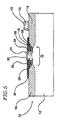
- FIG. 5 is a schematic cross-sectional view as in FIG. 4 illustrating the results of selectively removing the contact material from unwanted regions.
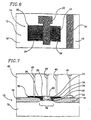
- FIG. 6 is a top view of the substrate and transistor structures in FIG. 5 showing the contact material extending partially over the isolation regions adjacent the source and drain regions, as well as a gate electrode structure and an interconnect electrode structure.
- FIG. 7 is a schematic cross-sectional view following subsequent processing to provide a passivation layer and electrical contacts.
- FIG. 8 is a schematic cross-sectional view illustrating an alternative method of planing using spin-on glass.
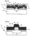
- FIG. 9 is a schematic cross-sectional view, similar to FIG. 2, illustrating the application of an alternative embodiment of the present invention to a trench isolated structure.
- FIG. 10 is a schematic cross-sectional view, similar to FIG. 5, illustrating the result of continuing the planing process to provide electrical isolation followed by selective patterning and etching.
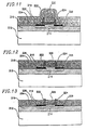
- FIG. 11 is a schematic cross-sectional view, similar to FIG. 2, illustrating the application of an alternative embodiment of the present invention to a SOI/SIMOX isolated structure without an electrode cap.
- FIG. 12 is a schematic cross-sectional view, similar to FIG. 4, illustrating the result of planing the contact material.
- FIG. 13 is a schematic cross-sectional view illustrating the result of etching the contact material and electrode to provide electrical isolation.
- FIG. 14 is a schematic cross-sectional view, similar to FIG. 5, illustrating the result of etching the contact material and electrode to provide electrical isolation followed by selective patterning and etching.
- FIG. 15 is a schematic cross-sectional view illustrating the deposition of silicidation material over polycrystalline silicon contact material.
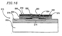
- FIG. 16 is a schematic cross-sectional view, similar to FIG. 5, illustrating the result of rapid thermal annealing to convert a polycrystalline silicon contact material into silicide.
- FIG. 17 is a flow chart summarizing the steps in the method of the present invention.
- FIG. 1 shows the result of several well known preliminary steps in the formation of metal oxide semiconductor (MOS) transistor structures 10 on a silicon substrate 12.
- MOS metal oxide semiconductor
- the processing of silicon substrate 12 includes isolating an active area 14 by bounding it with one or more isolation regions 16.
- isolation regions 16 One preferred structure for forming the isolation regions is a local-oxidation of silicon (LOCOS) structure.
- LOCS local-oxidation of silicon
- the gate electrode structure 19 typically includes a gate insulating layer 18 overlying silicon substrate 12.
- a gate electrode 20 overlies gate insulating layer 18.
- a first sidewall 22 and a second sidewall 24 are provided for isolation on either side of gate electrode 20,
- a source region 26 and a drain region 28 are formed by the implantation of doping impurities, either n + or p + , as is well known in the art.
- lightly doped drain/source (LDD) regions may also be formed prior to, or in conjunction with, formation of source region 26 and drain region 28.
- LDD lightly doped drain/source
- Interconnecting electrode structure 29 is formed on isolation regions 16 to provide connections to other active areas on the substrate (not shown).
- Interconnecting electrode structure 29 is intended to illustrate conductive interconnect lines and similar structures that, for example, could connect to, and be part of, a gate structure of an adjacent transistor (not shown).
- Interconnecting electrode structure 29 is formed in a manner similar to gate electrode structure 19, including an interconnecting electrode 30, first sidewall 31 and second sidewall 33.
- Electrode structures 19 and 29 as shown in FIGS. 1 - 3 include electrode caps 32 over electrodes 20 and 30. Electrode caps 32 are formed by depositing silicon dioxide, also known as oxide, or silicon nitride, photolithographic patterning and etching. Electrode caps 32 are present to protect underlying gate electrode 20 and interconnecting electrode 30 during subsequent processing. Although electrode caps 32 are preferable, especially in connection with LOCOS isolated structures, they are not required in all cases, as will be described below.
- the deposited contact material is preferably a refractory metal silicon compound, also known as silicide, formed by combining silicon and one or more metals selected from the group consisting of refractory and noble metals.
- Suitable examples of silicide materials used with the present invention include, TiSi 2 , TaSi 2 , WSi 2 , CoSi 2 , NiSi, or a combination thereof.
- contact material 34 is deposited over the entire wafer. It would, however, also be possible to apply contact material over only selected portions of the wafer. Contact material 34 is deposited to a thickness at least equal to the height of the highest electrode structure above silicon substrate 12. In FIG.
- interconnecting electrode structure 29 has a top 35 that is the highest electrode structure, because it is further from the surface of the substrate than any other structure.
- top 35 is the highest electrode structure, because it is further from the surface of the substrate than any other structure.
- the thickness is at least equal to the sum of thicknesses of gate insulating layer 18, gate electrode 20 and electrode cap 32 over the source/drain regions.
- Contact material 34 is deposited by any known method, including non-selective chemical vapor deposition (CVD).
- FIG. 3 shows MOS transistor structure 10 following leveling, also referred to herein as "planing", of contact material 34.
- Contact material 34 can be leveled using any appropriate planarization or etching process, including chemical mechanical polish (CMP) techniques.
- CMP chemical mechanical polish
- contact material 34 will be planarized using CMP until it is substantially level with the highest of the structures on silicon substrate 12, which as illustrated in FIG. 3 is top 35 of interconnecting electrode structure 29.
- other structures may be higher, although typically it will be either a gate electrode structure or an interconnecting electrode structure.
- electrodes 20 and 30 should be electrically isolated from contact material 34.
- a preferred method of electrically isolating the electrodes from the contact material is to etch the contact material back to a level no higher than the lowest electrode, whether a gate electrode or an interconnect electrode, This process is sometimes referred to herein as "etch back.”
- An etchant is used on the substrate and will typically etch the surfaces of all materials, but at different rates for different materials.
- the preferred method of etching contact material 34 is to use an etchant that has a selectivity of contact material to electrode cap material sufficient to etch back contact material 34 while allowing a sufficient portion of all gate electrodes 20 and interconnecting electrodes 30 to remain.
- contact material 34 will be etched back to a level such that a small portion of electrode caps 32 will remain.
- the selectivity is preferably sufficient to remove a thickness of contact material 34 at least equal to the sum of the thickness of one of the electrode caps 32 and the height of isolation regions 16 above silicon substrate 12, without completely removing any of the electrode caps 32.
- contact material 34 is no higher than the top of gate electrode 20.
- the minimum selectivity ratio which is the ratio of the etch rate of contact material to the etch rate of electrode caps 32, i.e. the etch rate of silicide to oxide or silicon nitride, is at least one in this embodiment, but preferably five or greater.
- contact material 34 has been planarized and etched back, contact material 34 remains substantially covering the entire wafer.
- Contact material 34 should then be removed from selected areas, in part, to allow for electrical isolation of adjacent structures, such as individual active devices.
- a suitable method of removing contact material 34 from selected areas is to apply photoresist to silicon substrate 12, as is well known in art. The photoresist is patterned to protect areas of contact material 34 that should remain following further processing. The unwanted contact material is then selectively etched to remove it. The remaining photoresist is then stripped, leaving only desired portions covered with contact material 34 as shown in FIGS. 5 and 6.
- the remaining contact material 34 preferably covers source region 26 and drain region 28 and extends over isolation regions 16 adjacent to each, forming source contact region 36 and drain contact region 38.
- the remaining contact material 34 preferably covers source region 26 and drain region 28 and extends over isolation regions 16 adjacent to each, forming source contact region 36 and drain contact region 38.
- FIG. 7 shows a cross-sectional view of a completed device, with electrical contacts 40 extending through a passivation layer 42 to contact source contact region 36, drain contact region 38, gate electrode 20, and interconnecting electrode 30.
- FIG. 8 shows an alternative method for leveling contact material 34.
- the step illustrated by FIG. 8 would occur between the steps described above with respect to FIGS. 2 and 3.
- a layer of glass 50 is spin coated over contact material 34.
- the glass fills in the troughs left by the contact material.
- the surface can then be etched such that the glass and the contact material are brought to a level approximating the level of the highest structure, similar to the results shown in FIG. 3.
- An etchant with an etch ratio of glass to contact material as close to one as possible should be used for this step. Since, an etchant with a glass to contact material etch ratio of exactly one is not known to applicants, the resulting surface using this alternative method will not be as level or uniform as the preferred CMP planarization method discussed previously.
- the resulting surface will instead be wavy and uneven. Although not ideal, this surface is still adequate for further processing according to the present invention.
- applying glass and subsequently etching the glass and contact material is considered a planing process, even though a smooth plane may not be produced.
- level does not require a perfectly flat or smooth plane, level refers to the elimination of the contact material above a desired height.
- the remaining steps of the present invention are as shown in FIGS. 4, 5, 6, and 7, as well as FIGS. 10, 13, 14, 15 and 16 described below.
- the method of the present invention can be performed on devices fabricated with a variety of isolation structures, including, trench isolated bulk silicon devices, mesa structures using silicon on insulator (SOI) structures or separation by implanted oxygen (SIMOX) structures.
- isolation structures including, trench isolated bulk silicon devices, mesa structures using silicon on insulator (SOI) structures or separation by implanted oxygen (SIMOX) structures.
- the electrical isolation may be obtained by etching back the contact material with an etchant that has a lower contact material to electrode cap etch ratio than in the first embodiment of FIGS 1-7.
- the contact material may only need to be etched an amount slightly greater than the thickness of the electrode caps.
- the selectivity ratio which is the ratio of the etch rate of electrode cap versus contact material, may be approximately one or greater in cases where there is only slight variation in the height of electrode structures.
- FIGS. 9-10 An alternative embodiment of processing in accordance with the present invention is shown in FIGS. 9-10.
- a MOS transistor structure 110 has been formed on a substrate 112 having an active area 114 bounded by trench isolation regions 116.
- FIG. 9, is analogous to FIG. 2 and shows an electrode structure 119 covered by a deposited contact material 134.
- the electrode structure 119 has tapered sidewalls 122 and 124 on either side of an electrode 120. The tapered sidewall 122 and 124 get thicker towards the substrate.
- the sidewalls are planed away along with the contact material, until a level is reached at which the sidewalls are thick enough to provide adequate electrical isolation between the electrode and the contact material. Accordingly, the contact material does not need to deposited to a height equal to the height of the electrode structure, but rather only to a height equal to or greater than the height at which the planing process is to be stopped. It should be noted that although an electrode cap 132 is shown, it is not necessary to the invention since the planing process in this embodiment of the invention removes electrode cap 132.
- FIG. 10 is analogous to FIG. 5, showing the results of planing the contact material, electrically isolating electrode 120 from contact material 134 by continued planing of electrode structures 119 and contact material 134, and subsequently selectively etching away a portion of the remaining contact material 134 to form a source contact region 136 and a drain contact region 138.
- MOS transistor structure 210 are formed on a SOI/SIMOX isolated structure having an isolation layer 216 overlying a silicon substrate 212.
- a source region 226 and a drain region 228 are formed within an active area 214 formed by depositing a layer of silicon over isolation layer 216 and doping the desired areas as is well known in the art.
- a SOI/SIMOX isolated structure and a trench isolated structure are generally interchangeable since the electrode structures are at approximately the same height.
- An electrode structure 219 is shown, having sidewalls 222 and 224 on either side of an electrode 220, but without an electrode cap.
- electrode 220 is a gate electrode.
- Contact material 234 has been deposited to a thickness at least equal to the height of electrode structure 219 above isolation layer 216. Contact material 234 is then planed until level, using CMP or other planing methodology disclosed herein, preferably stopping at the top of electrode structure 219 as shown in FIG. 12.
- electrode 220 and contact material 234 are electrically isolated by selectively etching using an etchant with a contact material to sidewall etch ratio of at least one.
- contact material 234 could be deposited silicide, as described above, here for illustration purposes contact material 234 and electrode 220 are both polycrystalline silicon, or poly. The other embodiments described above could also use polycrystalline silicon provided that the silicidation process described below is performed. Since electrode 220 and contact material 234 are the same material, poly, the etch ratio will be equal to one. However, the etch ratio of the contact material to the sidewalls should be greater than one. The etch should continue until the height of contact material 234 is low enough that sidewalls 222 and 224 are able to provide electrical isolation.
- FIG. 13 shows the sidewalls 222 and 224 with the upper portion removed for illustration purposes.
- electrical isolation is provided by the thickness of sidewalls 222 and 224 at the level of contact material 234, similar to the configuration shown in FIG. 10.
- contact material 234 remains, potentially covering the entire substrate.
- Contact material 234 should typically be removed from selected areas, in part, to allow for continued electrical isolation of adjacent structures.
- a photoresist can be applied to the silicon substrate and patterned, as is well known in the art. The unwanted contact material can then be selectively etched to remove it. The remaining photoresist can then be stripped, leaving only desired portions covered with contact material as shown in FIG. 14.
- the remaining contact material 234 covers source region 226, drain region 228 and extends over isolation region 216 adjacent to each forming a source contact region 236 and a drain contact region 238.
- a layer of silicidation material 260 is deposited over areas covered by contact material 234. Generally for ease of process, the silicidation material is deposited over the entire substrate.
- the silicidation material is selected from refractory metals and noble metals, including Co, Ti, Ni, W, Pt, Pd, Mo, Ta or a combination thereof.
- the next step is rapid thermal annealing. The substrate is annealed in a suitable annealing chamber at a temperature and for a duration sufficient to react the silicidation material with the underlying polycrystalline silicon material underneath to form a silicide layer 270. The temperatures and times are known by those skilled in the art. Where the silicidation material does not overly silicon, no silicidation occurs.
- the silicide lay 270 is formed, the remaining silicidation material is removed.
- the silicide layer 270 remains over the contact material 234, which is polycrystalline silicon.
- the combination of a layer of silicide over an underlying layer of polycrystalline silicon is referred to as a polycide.
- Polycide forms source contact region 236, drain contact ' region 238 and electrode 220.
- electrode 220 as shown is a gate electrode, the same process would apply to interconnecting electrodes (not shown).
- FIG. 16 shows the resulting structure following the silicidation process.
- the steps in the method of the present invention are illustrated schematically in FIG. 17.
- the first step 310 is to provide a substrate with appropriate transistor structures.
- Step 320 is depositing contact material over the substrate and structures.
- the contact material can be a deposited silicide material, a polycrystalline silicon (subject to a subsequent silicidation process) or other appropriate material.
- Step 330 is the planing of the deposited contact material and other structures, if necessary.
- the planing process is preferably accomplished using a CMP process, however, spin coating a layer of glass over the contact material and then etching the glass and contact material is also within the scope of the present invention.
- Step 340 is the electrical isolation of the electrodes from the contact material. This step can be accomplished by etching, or continued planing, depending on the variation in height of the electrode structures.
- Step 350 is the patterning and final etch step to remove contact material to allow for isolation of adjacent structures or active areas.
- the patterning and final etch also leaves contact material over the source region and the drain region to form a source contact region and a drain contact region.
Landscapes
- Electrodes Of Semiconductors (AREA)
- Insulated Gate Type Field-Effect Transistor (AREA)
- Thin Film Transistor (AREA)
- Internal Circuitry In Semiconductor Integrated Circuit Devices (AREA)
Abstract
Description
Claims (23)
- A method of forming MOS transistor structures on a silicon substrate comprising the steps of:a) defining a plurality of active areas on the substrate by forming one or more active area isolation regions, whereby adjacent active areas are isolated from each other;b) in each active area, forming source and drain regions;c) on the substrate, forming electrode structures comprising an electrode and insulating sidewalls;d) depositing contact material on the substrate and structures;e) planing; andf) in each active area, electrically isolating the electrode from the deposited contact material.
- The method as in claim 1, wherein the sidewalls are tapered and thinner at the top, and the source region, the drain region, and the electrode are electrically isolated by continuing the planing process to a level at which the sidewalls are thick enough to provide electrical isolation.
- The method as in claim 1, wherein the source region, the drain region, and the electrode are electrically isolated by selectively etching the contact material.
- The method as in claim 3, wherein the contact material is selectively etched with an etchant that etches the contact material at least as fast as the sidewalls until the contact material is etched to a level at which the sidewalls are thick enough to provide electrical isolation.
- The method as in claim 3, wherein the contact material is selectively etched with an etchant that etches the contact material faster than the sidewalls whereby a portion of the sidewalls extend higher than the contact material to provide electrical isolation,
- , The method as in claim 3, wherein the electrode structure further comprises electrode caps over the electrodes, and the contact material is selectively etched with an etchant that etches the contact material at least as fast as the electrode caps until the contact material reaches a level no higher than the lowest electrode.
- The method as in claim 6, wherein the etching step has a contact material to electrode cap etch ratio of at least 1.
- The method as in claim 6, wherein the isolation regions are formed by LOCOS isolated structure.
- The method as in claim 8, wherein the etching step has a contact material to electrode cap etch ratio larger than 5.
- The method as in claim 8, wherein the etching step has a contact material to electrode cap etch ratio sufficient to etch the contact material comprised of silicide to depth below the lowest electrode cap without completely etching away any electrode.
- The method as in claim 10, further comprising depositing silicidation material over the contact material comprised of polysilicon following removal of selected areas of the remaining polysilicon, rapid thermal annealing to form silicide in regions covered by polysilicon, whereby a polycide is formed over the regions covered by polysilicon, and removing remaining silicidation material.
- The method as in claim 1, wherein the silicidation material is at least one refractory metal.
- The method as in claim 12, wherein the silicidation material is at least one refractory metal selected from the group consisting of Co, Ti, Ni, W, Pt, Pd, Mo and Ta.
- The method as in claim 1, farther comprising removing selected areas of the remaining contact material to provide source/drain contact regions in each active area.
- The method as in claim 14, wherein the contact material is polysilicon.
- The method as in claim 14, wherein each source/drain contact region extends over a portion of the adjacent isolation regions, whereby the area of each source/drain contact region is larger than the respective source/drain region to facilitate subsequent interconnections.
- The method as in claim 1, wherein the contact material is applied over the entire substrate.
- The method as in claim 1, the contact material is at least one refractory metal silicon compound.
- The method as in claim 18, wherein the contact material is at least one refractory metal silicon compound chosen from the group consisting of TiSi2, TaSi2, WSi2, CoSi2 and NiSi.
- The method as in claim 1, wherein the planing is accomplished by chemical mechanical polish.
- A method of forming MOS transistor structures on a silicon substrate comprising the following steps:a) defining a plurality of active areas on the substrate by forming one or more active area isolation regions, whereby adjacent active areas are isolated from each other;b) in each active area, forming source and drain regions;c) forming electrodes on the substrate, including a gate electrode in each active area, and interconnect electrodes;d) forming insulating sidewalls along the gate electrode;e) forming silicon nitride electrode caps overlying the electrodes;f) depositing silicide over the entire substrate to a thickness sufficient to allow for subsequent planarization of the silicide layer;g) planing the silicide layer;h) selectively etching silicide to reduce silicide thickness to at least the level of the gate electrode without completely removing any electrode; andi) forming a mask pattern to define an area where silicide remains, including the source and drain regions in each active area, interconnects and a portion of the isolation regions adjacent to the source and drain regions, and removing unmasked silicide, whereby silicide extends from the source and drain regions over the adjacent isolation regions to provide a larger area for subsequent electrical connections.
- A MOS transistor structure formed on a silicon substrate comprising:a) a plurality of active areas on the substrate isolated from adjacent active areas by isolation regions;b) a source region, a drain region and a gate electrode within an active area;c) a source silicide region over the source region and extending over the isolation regions adjacent to the source region;d) a drain silicide region over the drain region and extending over the isolation regions adjacent to the drain region; ande) wherein the source silicide region and the drain silicide region do not extend above the gate electrode.
- A method of forming a contact to a device region of a MOS transistor structure provided on a substrate, said structure further including an electrode structure projecting from the substrate surface, the method including depositing a contact material on the substrate so as to cover the electrode structure, planing the contact material and reducing the thickness thereof so as to expose the electrode structure and electrically isolate it from the contact material, and selectively removing portions of the remaining contact material layer so as to leave a portion thereof which is electrically isolated from the electrode structure and is in contact with the device region.
Applications Claiming Priority (2)
| Application Number | Priority Date | Filing Date | Title |
|---|---|---|---|
| US09/497,626 US6352899B1 (en) | 2000-02-03 | 2000-02-03 | Raised silicide source/drain MOS transistors having enlarged source/drain contact regions and method |
| US497626 | 2000-02-03 |
Publications (2)
| Publication Number | Publication Date |
|---|---|
| EP1122771A2 true EP1122771A2 (en) | 2001-08-08 |
| EP1122771A3 EP1122771A3 (en) | 2001-11-28 |
Family
ID=23977627
Family Applications (1)
| Application Number | Title | Priority Date | Filing Date |
|---|---|---|---|
| EP01300938A Withdrawn EP1122771A3 (en) | 2000-02-03 | 2001-02-02 | Raised silicide source/drain MOS transistors and method |
Country Status (5)
| Country | Link |
|---|---|
| US (1) | US6352899B1 (en) |
| EP (1) | EP1122771A3 (en) |
| JP (1) | JP2001237427A (en) |
| KR (1) | KR100395734B1 (en) |
| TW (1) | TW480604B (en) |
Cited By (7)
| Publication number | Priority date | Publication date | Assignee | Title |
|---|---|---|---|---|
| DE102004004846A1 (en) * | 2004-01-30 | 2005-09-08 | Advanced Micro Devices, Inc., Sunnyvale | A method for depositing a layer of a material on a substrate |
| WO2007064473A1 (en) * | 2005-11-30 | 2007-06-07 | Advanced Micro Devices, Inc. | Low resistivity compound refractory metal silicides with high temperature stability |
| US7271455B2 (en) * | 2004-07-14 | 2007-09-18 | International Business Machines Corporation | Formation of fully silicided metal gate using dual self-aligned silicide process |
| US7340658B2 (en) | 2004-02-27 | 2008-03-04 | Advanced Micro Devices, Inc. | Technique for combining scan test and memory built-in self test |
| US9871059B2 (en) | 2011-12-23 | 2018-01-16 | Semiconductor Energy Laboratory Co., Ltd. | Semiconductor device and method for manufacturing the same |
| US10224433B2 (en) | 2011-11-30 | 2019-03-05 | Semiconductor Energy Laboratory Co., Ltd. | Method for manufacturing semiconductor device |
| TWI906253B (en) * | 2020-01-31 | 2025-12-01 | 美商蘭姆研究公司 | Alloy film etch |
Families Citing this family (5)
| Publication number | Priority date | Publication date | Assignee | Title |
|---|---|---|---|---|
| US7002208B2 (en) * | 2001-07-02 | 2006-02-21 | Oki Electric Industry Co., Ltd. | Semiconductor device and manufacturing method of the same |
| KR100403540B1 (en) * | 2001-12-22 | 2003-10-30 | 동부전자 주식회사 | Method For Manufacturing Semiconductor Devices |
| US7078298B2 (en) * | 2003-05-20 | 2006-07-18 | Sharp Laboratories Of America, Inc. | Silicon-on-nothing fabrication process |
| US7247530B2 (en) * | 2005-02-01 | 2007-07-24 | Sharp Laboratories Of America, Inc. | Ultrathin SOI transistor and method of making the same |
| KR102401486B1 (en) | 2015-04-22 | 2022-05-24 | 삼성전자주식회사 | A semiconductor device having a contact structure and method of manufacturing the semiconductor device |
Family Cites Families (15)
| Publication number | Priority date | Publication date | Assignee | Title |
|---|---|---|---|---|
| US4471522A (en) | 1980-07-08 | 1984-09-18 | International Business Machines Corporation | Self-aligned metal process for field effect transistor integrated circuits using polycrystalline silicon gate electrodes |
| FR2568723B1 (en) * | 1984-08-03 | 1987-06-05 | Commissariat Energie Atomique | INTEGRATED CIRCUIT, IN PARTICULAR OF THE MOS TYPE, AND ITS MANUFACTURING METHOD |
| JPH0628266B2 (en) * | 1986-07-09 | 1994-04-13 | 株式会社日立製作所 | Method for manufacturing semiconductor device |
| US5376578A (en) | 1993-12-17 | 1994-12-27 | International Business Machines Corporation | Method of fabricating a semiconductor device with raised diffusions and isolation |
| US5491099A (en) | 1994-08-29 | 1996-02-13 | United Microelectronics Corporation | Method of making silicided LDD with recess in semiconductor substrate |
| US5683924A (en) * | 1994-10-31 | 1997-11-04 | Sgs-Thomson Microelectronics, Inc. | Method of forming raised source/drain regions in a integrated circuit |
| US5516710A (en) | 1994-11-10 | 1996-05-14 | Northern Telecom Limited | Method of forming a transistor |
| US5571733A (en) * | 1995-05-12 | 1996-11-05 | Micron Technology, Inc. | Method of forming CMOS integrated circuitry |
| US5682055A (en) * | 1995-06-07 | 1997-10-28 | Sgs-Thomson Microelectronics, Inc. | Method of forming planarized structures in an integrated circuit |
| US5804846A (en) * | 1996-05-28 | 1998-09-08 | Harris Corporation | Process for forming a self-aligned raised source/drain MOS device and device therefrom |
| US5830775A (en) | 1996-11-26 | 1998-11-03 | Sharp Microelectronics Technology, Inc. | Raised silicided source/drain electrode formation with reduced substrate silicon consumption |
| US5918132A (en) | 1996-12-31 | 1999-06-29 | Intel Corporation | Method for narrow space formation and self-aligned channel implant |
| US5866459A (en) | 1997-02-20 | 1999-02-02 | National Semiconductor Corporation | Method of fabricating a contact structure for an MOS transistor entirely on isolation oxide |
| US5998269A (en) * | 1998-03-05 | 1999-12-07 | Taiwan Semiconductor Manufacturing Company, Ltd. | Technology for high performance buried contact and tungsten polycide gate integration |
| US5915183A (en) | 1998-06-26 | 1999-06-22 | International Business Machines Corporation | Raised source/drain using recess etch of polysilicon |
-
2000
- 2000-02-03 US US09/497,626 patent/US6352899B1/en not_active Expired - Fee Related
-
2001
- 2001-02-02 EP EP01300938A patent/EP1122771A3/en not_active Withdrawn
- 2001-02-02 JP JP2001027567A patent/JP2001237427A/en not_active Withdrawn
- 2001-02-03 KR KR10-2001-0005263A patent/KR100395734B1/en not_active Expired - Fee Related
- 2001-02-05 TW TW090102359A patent/TW480604B/en not_active IP Right Cessation
Cited By (10)
| Publication number | Priority date | Publication date | Assignee | Title |
|---|---|---|---|---|
| DE102004004846A1 (en) * | 2004-01-30 | 2005-09-08 | Advanced Micro Devices, Inc., Sunnyvale | A method for depositing a layer of a material on a substrate |
| DE102004004846B4 (en) * | 2004-01-30 | 2006-06-14 | Advanced Micro Devices, Inc., Sunnyvale | A method for depositing a layer of a material on a substrate |
| US7338872B2 (en) | 2004-01-30 | 2008-03-04 | Advanced Micro Devices, Inc. | Method of depositing a layer of a material on a substrate |
| US7340658B2 (en) | 2004-02-27 | 2008-03-04 | Advanced Micro Devices, Inc. | Technique for combining scan test and memory built-in self test |
| US7271455B2 (en) * | 2004-07-14 | 2007-09-18 | International Business Machines Corporation | Formation of fully silicided metal gate using dual self-aligned silicide process |
| US7785999B2 (en) | 2004-07-14 | 2010-08-31 | International Business Machines Corporation | Formation of fully silicided metal gate using dual self-aligned silicide process |
| WO2007064473A1 (en) * | 2005-11-30 | 2007-06-07 | Advanced Micro Devices, Inc. | Low resistivity compound refractory metal silicides with high temperature stability |
| US10224433B2 (en) | 2011-11-30 | 2019-03-05 | Semiconductor Energy Laboratory Co., Ltd. | Method for manufacturing semiconductor device |
| US9871059B2 (en) | 2011-12-23 | 2018-01-16 | Semiconductor Energy Laboratory Co., Ltd. | Semiconductor device and method for manufacturing the same |
| TWI906253B (en) * | 2020-01-31 | 2025-12-01 | 美商蘭姆研究公司 | Alloy film etch |
Also Published As
| Publication number | Publication date |
|---|---|
| KR20010078326A (en) | 2001-08-20 |
| KR100395734B1 (en) | 2003-08-25 |
| EP1122771A3 (en) | 2001-11-28 |
| JP2001237427A (en) | 2001-08-31 |
| TW480604B (en) | 2002-03-21 |
| US6352899B1 (en) | 2002-03-05 |
Similar Documents
| Publication | Publication Date | Title |
|---|---|---|
| US6153485A (en) | Salicide formation on narrow poly lines by pulling back of spacer | |
| US5780349A (en) | Self-aligned MOSFET gate/source/drain salicide formation | |
| US5464782A (en) | Method to ensure isolation between source-drain and gate electrode using self aligned silicidation | |
| US7211515B2 (en) | Methods of forming silicide layers on source/drain regions of MOS transistors | |
| US5736419A (en) | Method of fabricating a raised source/drain MOSFET using self-aligned POCl3 for doping gate/source/drain regions | |
| US7067379B2 (en) | Silicide gate transistors and method of manufacture | |
| US5744395A (en) | Low resistance, self-aligned, titanium silicide structures, using a single rapid thermal anneal procedure | |
| US6657244B1 (en) | Structure and method to reduce silicon substrate consumption and improve gate sheet resistance during silicide formation | |
| US6806534B2 (en) | Damascene method for improved MOS transistor | |
| CN100461463C (en) | Semiconductor structure and method of forming a metal oxide semiconductor structure | |
| JPH1126757A (en) | Semiconductor device and manufacturing method thereof | |
| US6258648B1 (en) | Selective salicide process by reformation of silicon nitride sidewall spacers | |
| EP0849783A2 (en) | Directionally deposited silicide on transistor electrodes and method for same | |
| US20070222000A1 (en) | Method of forming silicided gate structure | |
| US6271133B1 (en) | Optimized Co/Ti-salicide scheme for shallow junction deep sub-micron device fabrication | |
| US6352899B1 (en) | Raised silicide source/drain MOS transistors having enlarged source/drain contact regions and method | |
| US6838366B2 (en) | MOS transistors and methods for manufacturing the same | |
| US6232188B1 (en) | CMP-free disposable gate process | |
| US5866459A (en) | Method of fabricating a contact structure for an MOS transistor entirely on isolation oxide | |
| US6395606B1 (en) | MOSFET with metal in gate for reduced gate resistance | |
| US5858846A (en) | Salicide integration method | |
| US6653227B1 (en) | Method of cobalt silicidation using an oxide-Titanium interlayer | |
| JPH08213610A (en) | Field effect type semiconductor device and method of manufacturing the same | |
| US7563700B2 (en) | Method for improving self-aligned silicide extendibility with spacer recess using an aggregated spacer recess etch (ASRE) integration | |
| US6218690B1 (en) | Transistor having reverse self-aligned structure |
Legal Events
| Date | Code | Title | Description |
|---|---|---|---|
| PUAI | Public reference made under article 153(3) epc to a published international application that has entered the european phase |
Free format text: ORIGINAL CODE: 0009012 |
|
| AK | Designated contracting states |
Kind code of ref document: A2 Designated state(s): DE FR GB Kind code of ref document: A2 Designated state(s): AT BE CH CY DE DK ES FI FR GB GR IE IT LI LU MC NL PT SE TR |
|
| AX | Request for extension of the european patent |
Free format text: AL;LT;LV;MK;RO;SI |
|
| PUAL | Search report despatched |
Free format text: ORIGINAL CODE: 0009013 |
|
| AK | Designated contracting states |
Kind code of ref document: A3 Designated state(s): AT BE CH CY DE DK ES FI FR GB GR IE IT LI LU MC NL PT SE TR |
|
| AX | Request for extension of the european patent |
Free format text: AL;LT;LV;MK;RO;SI |
|
| 17P | Request for examination filed |
Effective date: 20020307 |
|
| AKX | Designation fees paid |
Free format text: AT BE CH LI |
|
| RBV | Designated contracting states (corrected) |
Designated state(s): DE FR GB |
|
| REG | Reference to a national code |
Ref country code: DE Ref legal event code: 8566 |
|
| 17Q | First examination report despatched |
Effective date: 20080610 |
|
| STAA | Information on the status of an ep patent application or granted ep patent |
Free format text: STATUS: THE APPLICATION IS DEEMED TO BE WITHDRAWN |
|
| 18D | Application deemed to be withdrawn |
Effective date: 20081021 |