EP1122579A2 - Scanning optical device and image forming apparatus - Google Patents
Scanning optical device and image forming apparatus Download PDFInfo
- Publication number
- EP1122579A2 EP1122579A2 EP01101721A EP01101721A EP1122579A2 EP 1122579 A2 EP1122579 A2 EP 1122579A2 EP 01101721 A EP01101721 A EP 01101721A EP 01101721 A EP01101721 A EP 01101721A EP 1122579 A2 EP1122579 A2 EP 1122579A2
- Authority
- EP
- European Patent Office
- Prior art keywords
- scanning direction
- variation
- caused
- imaging position
- scanning optical
- Prior art date
- Legal status (The legal status is an assumption and is not a legal conclusion. Google has not performed a legal analysis and makes no representation as to the accuracy of the status listed.)
- Granted
Links
Images









Classifications
-
- G—PHYSICS
- G02—OPTICS
- G02B—OPTICAL ELEMENTS, SYSTEMS OR APPARATUS
- G02B27/00—Optical systems or apparatus not provided for by any of the groups G02B1/00 - G02B26/00, G02B30/00
- G02B27/42—Diffraction optics, i.e. systems including a diffractive element being designed for providing a diffractive effect
- G02B27/4205—Diffraction optics, i.e. systems including a diffractive element being designed for providing a diffractive effect having a diffractive optical element [DOE] contributing to image formation, e.g. whereby modulation transfer function MTF or optical aberrations are relevant
- G02B27/4211—Diffraction optics, i.e. systems including a diffractive element being designed for providing a diffractive effect having a diffractive optical element [DOE] contributing to image formation, e.g. whereby modulation transfer function MTF or optical aberrations are relevant correcting chromatic aberrations
-
- G—PHYSICS
- G02—OPTICS
- G02B—OPTICAL ELEMENTS, SYSTEMS OR APPARATUS
- G02B26/00—Optical devices or arrangements for the control of light using movable or deformable optical elements
- G02B26/08—Optical devices or arrangements for the control of light using movable or deformable optical elements for controlling the direction of light
- G02B26/10—Scanning systems
- G02B26/12—Scanning systems using multifaceted mirrors
- G02B26/125—Details of the optical system between the polygonal mirror and the image plane
-
- G—PHYSICS
- G02—OPTICS
- G02B—OPTICAL ELEMENTS, SYSTEMS OR APPARATUS
- G02B27/00—Optical systems or apparatus not provided for by any of the groups G02B1/00 - G02B26/00, G02B30/00
- G02B27/0025—Optical systems or apparatus not provided for by any of the groups G02B1/00 - G02B26/00, G02B30/00 for optical correction, e.g. distorsion, aberration
- G02B27/0031—Optical systems or apparatus not provided for by any of the groups G02B1/00 - G02B26/00, G02B30/00 for optical correction, e.g. distorsion, aberration for scanning purposes
-
- G—PHYSICS
- G02—OPTICS
- G02B—OPTICAL ELEMENTS, SYSTEMS OR APPARATUS
- G02B27/00—Optical systems or apparatus not provided for by any of the groups G02B1/00 - G02B26/00, G02B30/00
- G02B27/0025—Optical systems or apparatus not provided for by any of the groups G02B1/00 - G02B26/00, G02B30/00 for optical correction, e.g. distorsion, aberration
- G02B27/0037—Optical systems or apparatus not provided for by any of the groups G02B1/00 - G02B26/00, G02B30/00 for optical correction, e.g. distorsion, aberration with diffracting elements
-
- G—PHYSICS
- G02—OPTICS
- G02B—OPTICAL ELEMENTS, SYSTEMS OR APPARATUS
- G02B27/00—Optical systems or apparatus not provided for by any of the groups G02B1/00 - G02B26/00, G02B30/00
- G02B27/42—Diffraction optics, i.e. systems including a diffractive element being designed for providing a diffractive effect
- G02B27/4205—Diffraction optics, i.e. systems including a diffractive element being designed for providing a diffractive effect having a diffractive optical element [DOE] contributing to image formation, e.g. whereby modulation transfer function MTF or optical aberrations are relevant
- G02B27/4216—Diffraction optics, i.e. systems including a diffractive element being designed for providing a diffractive effect having a diffractive optical element [DOE] contributing to image formation, e.g. whereby modulation transfer function MTF or optical aberrations are relevant correcting geometrical aberrations
-
- G—PHYSICS
- G02—OPTICS
- G02B—OPTICAL ELEMENTS, SYSTEMS OR APPARATUS
- G02B27/00—Optical systems or apparatus not provided for by any of the groups G02B1/00 - G02B26/00, G02B30/00
- G02B27/42—Diffraction optics, i.e. systems including a diffractive element being designed for providing a diffractive effect
- G02B27/4205—Diffraction optics, i.e. systems including a diffractive element being designed for providing a diffractive effect having a diffractive optical element [DOE] contributing to image formation, e.g. whereby modulation transfer function MTF or optical aberrations are relevant
- G02B27/4227—Diffraction optics, i.e. systems including a diffractive element being designed for providing a diffractive effect having a diffractive optical element [DOE] contributing to image formation, e.g. whereby modulation transfer function MTF or optical aberrations are relevant in image scanning systems
-
- G—PHYSICS
- G02—OPTICS
- G02B—OPTICAL ELEMENTS, SYSTEMS OR APPARATUS
- G02B27/00—Optical systems or apparatus not provided for by any of the groups G02B1/00 - G02B26/00, G02B30/00
- G02B27/42—Diffraction optics, i.e. systems including a diffractive element being designed for providing a diffractive effect
- G02B27/4283—Diffraction optics, i.e. systems including a diffractive element being designed for providing a diffractive effect having a diffractive element with major temperature dependent properties
Definitions
- the present invention relates to a scanning optical device and image forming apparatus and, more particularly, to a compact image forming apparatus suitable for high-resolution printing with, e.g., a color electrophotographic process, such as a laser beam printer (LBP) or color digital copying machine, in which an imaging position variation caused by the wavelength fluctuation of a light source means, an aberration variation upon an environmental fluctuation, and the like in each scanning optical device are compensated by a compensation means in a color image forming apparatus having a plurality of scanning optical devices, thereby suppressing an imaging position deviation in especially the main scanning direction, and reducing color misregistration, and image density nonuniformity at low cost with a simple arrangement.
- a color electrophotographic process such as a laser beam printer (LBP) or color digital copying machine
- a beam modulated and emitted by a light source means in accordance with an image signal is periodically deflected by an optical deflector formed from, e.g., a rotary polyhedral mirror (polygon mirror), and converged into a spot on a photosensitive recording medium (photosensitive drum) surface by an imaging optical system (scanning optical system) having an f- ⁇ characteristic.
- an optical deflector formed from, e.g., a rotary polyhedral mirror (polygon mirror), and converged into a spot on a photosensitive recording medium (photosensitive drum) surface by an imaging optical system (scanning optical system) having an f- ⁇ characteristic. This surface is optically scanned to record an image.
- Fig. 24 is a schematic view showing the main part of a conventional scanning optical device.
- a divergent beam emitted by a light source means 91 is converted into a nearly collimated beam by a collimator lens 92.
- the beam is limited by a stop 93, and enters a cylindrical lens 94 having a predetermined refracting power in only the sub scanning direction.
- a cylindrical lens 94 having a predetermined refracting power in only the sub scanning direction.
- light components in the main scanning plane directly emerge as a nearly collimated beam.
- light components are converged to form an almost line image on a deflection surface (reflection surface) 95a of an optical deflector 95 formed from a rotary polyhedral mirror (polygon mirror).
- the beam deflected and reflected by the deflection surface 95a of the optical deflector 95 is guided onto a photosensitive drum surface 98 as a surface to be scanned via an imaging optical element (f- ⁇ lens) 96 having f- ⁇ characteristics.
- an imaging optical element (f- ⁇ lens) 96 having f- ⁇ characteristics.
- Fig. 25 is a schematic view showing the main part of a conventional color image forming apparatus.
- the color image forming apparatus simultaneously uses a plurality of scanning optical devices 111 to 114 like the above-described one to record pieces of image information of respective colors on corresponding photosensitive drums 121 to 124, thereby forming a color image.
- this color image forming apparatus it is important to reduce not only an imaging position deviation represented by jitter of a single color but also scanning line deviations (to be referred to as "misregistration" hereinafter) between colors, and image density nonuniformity between colors in order to align a plurality of scanning lines and form an image.
- the scanning optical device must satisfy the following conditions.
- jitter by a plurality of beams occurs owing to the wavelength difference between the light-emitting portions, greatly degrading the image quality.
- (1) compensation of a spot position deviation and (4) compensation of a spot imaging position deviation not accompanied by any environmental fluctuation become more important.
- Such a scanning optical device has conventionally used a glass lens or glass mirror which hardly exhibits a characteristic fluctuation caused by an environmental fluctuation.
- an aberration variation caused by the wavelength fluctuation of a semiconductor laser remains, advanced aberration correction by an aspherical surface cannot be performed, and the cost is high.
- demands have arisen for compensation of a wavelength fluctuation, environmental fluctuation, or the like by a scanning optical device using a plastic material.
- Japanese Patent Application Laid-Open No. 3-231218 discloses a scanning optical device in which a scanning optical system is constituted by a glass spherical lens and plastic toric lens.
- a scanning optical system is constituted by a glass spherical lens and plastic toric lens.
- an imaging position deviation in the main scanning direction caused by a wavelength variation of 5 nm is 64.6 ⁇ m
- a focus deviation in the sub scanning direction at a temperature elevated by 25°C is +1.7 mm.
- a color image forming apparatus using a plurality of such scanning optical devices suffers misregistration or image nonuniformity between colors.
- Japanese Patent Application Laid-Open No. 7-128603 discloses an example in which a glass lens and glass cylinder mirror are used as the scanning optical system of a scanning optical device used in a color image forming apparatus.
- all the scanning optical systems are made of a glass material.
- An aberration variation caused by the wavelength fluctuation of a semiconductor laser remains.
- Aberration correction by an aspherical surface cannot be performed, so the optical path is long.
- the cost is high.
- Japanese Patent Application Laid-Open No. 10-232347 discloses an example in which a scanning optical system is formed from two toric lenses.
- all the scanning optical systems are made of a plastic, which is advantageous for aberration correction.
- the laser wavelength increases as the temperature is elevated.
- the refractive index of the scanning optical system decreases, the laser wavelength varies in a direction in which the focal length of a scanning lens increases. As a result, the imaging position in the main scanning direction greatly deviates.
- a scanning optical device comprises light source means, and an optical element having a refraction element and a diffraction element, wherein powers of said refraction element and said diffraction element are set such that an imaging position deviation in a main scanning direction on a surface to be scanned that is caused by a wavelength variation of a beam emitted by said light source means along with an environmental fluctuation of said scanning optical device, and an imaging position deviation in the main scanning direction on the surface to be scanned that is caused by a refractive index variation of a material of said optical element along with an environmental fluctuation are set to be in opposite directions at two ends of an effective scanning region.
- said optical element includes an element which forms the beam emitted by said light source means into an image on the surface to be scanned, and letting ⁇ Lm and ⁇ Dm be powers of said refraction element and diffraction element constituting said optical element in the main scanning direction, and ⁇ L be an Abbe number of a material of said refraction element, the powers satisfy a condition: ⁇ L/6.90 ⁇ ⁇ Lm/ ⁇ Dm ⁇ ⁇ L/3.45
- an imaging position variation per unit mode hopping of said light source means is not more than 3 ⁇ m at the two ends of the effective scanning region.
- a focus position deviation in a sub scanning direction on the surface to be scanned that is caused by the wavelength variation of the beam emitted by said light source means along with the environmental fluctuation, and a focus position deviation in the sub scanning direction on the surface to be scanned that is caused by the refractive index variation of the material of said optical element along with the environmental fluctuation are substantially compensated within the effective scanning region.
- the environmental fluctuation includes an atmospheric variation of said scanning optical device and a temperature variation caused by self-temperature elevation.
- said refraction element includes a toric lens
- said diffraction element includes a composite optical element obtained by integrating a refraction surface and a diffraction surface.
- said refraction element and diffraction element constituting said optical element are formed from a plastic material.
- said light source means includes a multi-beam laser source having a plurality of light-emitting portions.
- ⁇ Ls and ⁇ Ds be powers of said refraction element and diffraction element constituting said optical element in a sub scanning direction, the powers satisfy a condition: 1.0 ⁇ ⁇ Ls/ ⁇ Ds ⁇ 2.6
- the powers of said refraction element and said diffraction element are set to compensate for an imaging position variation in the main scanning direction on the surface to be scanned that is caused by a wavelength fluctuation of the beam emitted by said light source means.
- an image forming apparatus comprises a plurality of pairs of scanning optical devices defined in claim 1 and corresponding image carriers, guides beams emitted by said scanning optical devices to corresponding image carriers, scans surfaces of said image carriers to form images of different colors on the surfaces of said image carriers, and forms a color image by the images formed on the surfaces of said image carriers.
- a scanning optical device guides a beam emitted by light source means to a surface to be scanned, and scans the surface with the beam
- said scanning optical device comprises compensation means having a refraction element and a diffraction element so as to compensate for an imaging position deviation in a main scanning direction on the surface to be scanned that is caused by a wavelength fluctuation of the beam emitted by said light source means, and letting ⁇ Lm and ⁇ Dm be powers of said refraction element and said diffraction element in the main scanning direction, the powers satisfy a condition: 5.8 ⁇ ⁇ Lm/ ⁇ Dm ⁇ 20
- a focus position variation in a sub scanning direction on the surface to be scanned that is caused by an environmental fluctuation of said scanning optical device is compensated by power variations of said refraction element and said diffraction element, and a wavelength variation of the beam emitted by said light source means.
- said refraction element is formed from a plastic material.
- said compensation means includes means for forming the beam emitted by said light source means into an image on the surface to be scanned.
- said light source means includes a multi-beam laser source having a plurality of light-emitting portions.
- said compensation means includes means for compensating for an imaging position variation in the main scanning direction on the surface to be scanned that is caused by the wavelength fluctuation of the beam emitted by said light source means, and a scanning interval fluctuation in the main scanning direction on the surface to be scanned that is caused by a wavelength difference between beams emitted by a plurality of light-emitting portions.
- an image forming apparatus comprises a plurality of pairs of scanning optical devices set out in the foregoing and corresponding image carriers, guides beams emitted by said scanning optical devices to corresponding image carriers, scans surfaces of said image carriers to form images of different colors on the surfaces of said image carriers, and forms a color image by the images formed on the surfaces of said image carriers.
- an image forming apparatus comprises a scanning optical device set out in the foregoing and a printer controller for converting code data input from an external device into an image signal and inputting the converted image signal to said scanning optical device.
- Fig. 1 is a schematic view showing the main part of a color image forming apparatus according to the first embodiment of the present invention.
- scanning optical devices 11, 12, 13, and 14, photosensitive drums 21, 22, 23, and 24 serving as image carriers, and developing units 31, 32, 33, and 34 are arranged along a convey belt 41.
- the four scanning optical devices (11, 12, 13, and 14) in which an imaging position variation caused by the wavelength fluctuation of a beam emitted by a light source (to be simply referred to as the "wavelength fluctuation of the light source” hereinafter) or an aberration variation upon an environmental variation (temperature variation) are arranged respectively correspond to four, C (Cyan), M (Magenta), Y (Yellow), and B (Black) colors, and record image signals (image information) on the surfaces of the photosensitive drums 21, 22, 23, and 24 in parallel with each other, thereby printing a color image at a high speed.
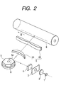
- Fig. 2 is a schematic view showing the main part of one scanning optical device and a corresponding image carrier
- Fig. 3 is a sectional view (sectional view of main scanning) showing the main part of the optical system shown in Fig. 2 in the main scanning direction.
- a light source means (laser source) 1 is formed from, e.g., a semiconductor laser.
- a collimator lens 2 serving as a first optical element converts a divergent beam emitted by the light source means 1 into a nearly collimated beam.
- An aperture stop 3 limits a passing beam (light quantity).
- a cylindrical lens (cylinder lens) 4 serving as a second optical element has a predetermined refracting power in only the sub scanning direction, and forms the beam having passed through the aperture stop 3 into an almost line image on a deflection surface (reflection surface) 5a of an optical deflector 5 (to be described later).
- the optical deflector 5 serving as a deflection element is formed from, e.g., a polygon mirror (rotary polyhedral mirror), and rotated by a driving means (not shown) such as a motor at a predetermined speed in a direction indicated by an arrow A in Fig. 2.
- a driving means such as a motor at a predetermined speed in a direction indicated by an arrow A in Fig. 2.
- a scanning optical element 6 as a third optical element (compensation means) having an f- ⁇ characteristic has a refraction element 61 and diffraction element 62.
- the refraction element 61 is formed from a single plastic toric lens having different powers in the main scanning direction and sub scanning direction. Two lens surfaces 61a and 61b of the toric lens 61 in the main scanning direction are aspherical.
- the diffraction element 62 is formed from an elongated composite optical element having different powers in the main scanning direction and sub scanning direction.
- An incident-side surface 62a of the composite optical element 62 is an aspherical surface having a predetermined power in only the main scanning direction (surface in the sub scanning direction is flat), whereas an exit-side surface 62b is a diffraction surface with a diffraction grating 81 added to a flat surface.
- the grating shape of the diffraction grating 81 is preferably a Fresnel grating shape of a sawtooth-like diffraction grating by surface cutting, or a stepped diffraction grating shape by photoetching.
- the composite optical element 62 in this embodiment is made of a plastic prepared by injection molding. The same effects can also be obtained by forming a diffraction grating from a replica on a glass substrate.
- the toric lens 61 is disposed on the polygon mirror 5 side with respect to the midpoint between the rotating shaft of the polygon mirror 5 and a surface 8 to be scanned, and the composite optical element 62 is disposed on the surface 8 side.
- Each optical element has different powers in the main scanning direction and sub scanning direction, as described above. These optical elements form a deflected beam from the polygon mirror 5 into an image on the surface 8, and correct the face tangle error of the deflection surface of the polygon mirror.
- the surface 8 to be scanned is a photosensitive drum surface.
- the color image forming apparatus in this embodiment forms latent images on the surfaces of the corresponding photosensitive drums 21, 22, 23, and 24 by the four scanning optical devices 11, 12, 13, and 14 using beams based on modulated signals.
- the color image forming apparatus forms C (Cyan), M (Magenta), Y (Yellow), and B (Black) latent images on the surfaces of the corresponding photosensitive drums 21, 22, 23, and 24, and multiple-transfers the latent images on a recording medium to form one full-color image.
- a divergent beam emitted by the semiconductor laser 1 is converted into a nearly collimated beam by the collimator lens 2.
- the beam (light quantity) is limited by the aperture stop, and enters the cylindrical lens 4.
- the nearly collimated beam that enters the cylindrical lens 4 light components in the main scanning section directly emerge as a nearly collimated beam.
- the sub scanning section light components are converged to form an almost line image (elongated line image in the main scanning direction) on the deflection surface 5a of the optical deflector 5.
- the beam deflected by the deflection surface 5a of the optical deflector 5 is guided onto the photosensitive drum surface 8 via the toric lens 61 and composite optical element 62.
- the beam scans the photosensitive drum surface 8 in a direction indicated by an arrow B (main scanning direction).
- C Cyan
- M Magnetic
- Y Yellow
- B Black
- the toric lens 61 and composite optical element 62 which constitute the third optical element (scanning optical element) 6 of the scanning optical device in the first embodiment have the following shapes.
- the intersection between the refraction surface and the optical axis is defined as the origin.
- the x-axis is set along the optical axis direction
- the y-axis is set along an axis perpendicular to the optical axis in the main scanning section
- the z-axis is set along an axis perpendicular to the optical axis in the sub scanning section.
- the power layout of the toric lens 61 made of a plastic (polyolefin material: available from Zeonex) and the composite optical element 62 can be appropriately set to compensate for both an imaging position variation caused by the wavelength fluctuation of the light source in the main scanning direction and a focus variation caused by the environmental fluctuation (particularly temperature elevation) of the device in the sub scanning direction.
- the chromatic aberration of magnification of the scanning optical system is compensated in the main scanning direction by the refraction element (refraction portion) 61 having a positive dispersion and the diffraction element (diffraction portion) 62 having a negative dispersion (chromatic compensation of magnification).
- the Abbe number has a limited range of values.
- the power ratio of the refraction element 61 to the diffraction element 62 in the main scanning direction desirably satisfies a condition: 5.8 ⁇ ⁇ Lm/ ⁇ Dm ⁇ 20
- Condition (1) is related to the power ratio of the refraction element 61 to the diffraction element 62 in the main scanning direction that constitute the scanning optical element 6.
- a power layout which does not satisfy condition (1) is undesirable because it becomes difficult to correct an imaging position variation in the main scanning direction on the surface 8 to be scanned that is caused by the wavelength variation of the semiconductor laser 1.
- the refractive index variation of the optical element caused by the environmental fluctuation (particularly temperature elevation) of the device is compensated by the wavelength variation of the semiconductor laser 1 caused by the same environmental fluctuation, thereby canceling focus movement (temperature compensation).
- the power layout is desirably set to 1.0 ⁇ ⁇ Ls/ ⁇ Ds ⁇ 2.6 where
- Condition (2) is related to the power ratio of the refraction element 61 to the diffraction element 62 in the sub scanning direction that constitute the scanning optical element 6.
- a power layout which does not satisfy condition (2) is undesirable because it becomes difficult to correct a focus variation in the sub scanning direction along with the environmental fluctuation of the scanning optical device.
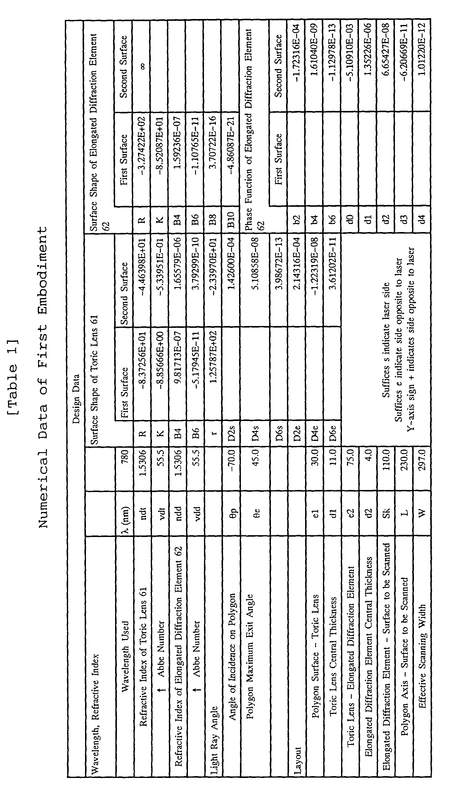
- Table 1 shows the optical layout in the first embodiment, aspherical coefficients of the toric lens 61, and aspherical coefficients and phase terms of the composite optical element 62.
- Fig. 4 is a graph showing an imaging position variation in the main scanning direction caused by the wavelength variation of the semiconductor laser 1 in the first embodiment.
- Fig. 4 shows a difference (5 nm) from the initial wavelength of the semiconductor laser 1.
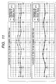
- Fig. 5 is a graph showing paraxial aberration (curvature of field in the main scanning direction and sub scanning direction) before and after an environmental fluctuation in the first embodiment.
- the solid line represents a characteristic (design value) before an environmental fluctuation, and the broken line represents a characteristic (effective value) when the temperature is elevated by 25°C.
- an imaging position deviation in the main scanning direction caused by the wavelength fluctuation of a semiconductor laser must be suppressed to 50 ⁇ m or less, and focus deviations in the main scanning direction and sub scanning direction caused by the environmental fluctuation (temperature fluctuation) of the device must be suppressed to ⁇ 1.0 mm or less, in order that misregistration between colors and image density nonuniformity between colors may be visually inconspicuous.
- an imaging position deviation caused by a wavelength difference of +5 nm is 41 ⁇ m in the first embodiment, and corresponds to a pixel (position) deviation suppressed within about one pixel in, e.g., a printer having a resolution of 600 dpi.
- the initial wavelength deviation of a semiconductor laser between a plurality of colors, or mode hopping in activation is permitted by about 5 nm.
- the initial wavelength deviation of a semiconductor laser between a plurality of colors means the individual difference between the wavelengths of respective semiconductor lasers in an image forming apparatus (so-called 4-drum color printer) which scans a plurality of image carrier surfaces with beams from a plurality of scanning optical devices.
- the focus movement amount in the sub scanning direction at a temperature elevated by 25°C is 0.2 mm, and is suppressed to a visually negligible level both in the sub scanning direction and main scanning direction.
- the first embodiment compensates for all these environmental fluctuations using a plastic optical element. This can simultaneously reduce the manufacturing cost by molding and shorten the optical path by large-field-angle aberration correction using an aspherical surface.
- the first embodiment uses the plastic toric lens 61 and composite optical element 62 as the scanning optical element 6 of the scanning optical device, and records images on a plurality of photosensitive drums by a plurality of scanning optical devices.
- a color image forming apparatus in which misregistration between colors caused by a wavelength fluctuation or environmental fluctuation, and density nonuniformity between colors are reduced can be implemented with a simple arrangement at low cost.
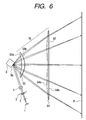
- Fig. 6 is a sectional view of the main part of an optical system in the main scanning direction showing one of a plurality of scanning optical devices constituting a color image forming apparatus according to the second embodiment of the present invention, and a corresponding photosensitive drum.
- the same reference numerals as in Fig. 3 denote the same parts.
- the second embodiment is different from the first embodiment in that a plastic toric lens as a refraction element is made of a material such as polycarbonate (PC) having a large dispersion, and that the power ratio of the refraction element to the diffraction element is optimized along with this change.
- PC polycarbonate
- a scanning optical element 16 as a third optical element (compensation means) having an f- ⁇ characteristic has a refraction element 63 and diffraction element 64.
- the refraction element 63 is formed from a single plastic toric lens of a material such as polycarbonate (PC) having a large dispersion with different powers in the main scanning direction and sub scanning direction.
- Two lens surfaces 63a and 63b of the toric lens 63 in the main scanning direction are aspherical.
- the diffraction element 64 is formed from an elongated composite optical element having different powers in the main scanning direction and sub scanning direction.
- An incident-side surface 64a of the composite optical element 64 is an aspherical surface having a predetermined power in only the main scanning direction (surface in the sub scanning direction is flat), whereas an exit-side surface 64b is a diffraction surface with a diffraction grating 82 added to a flat surface.
- Table 2 shows the optical layout in the second embodiment, aspherical coefficients of the toric lens 63, and aspherical coefficients and phase terms of the composite optical element 64.
- the power layout of the plastic toric lens 63 and composite optical element 64 can be appropriately set to compensate for both an imaging position variation caused by the wavelength variation of a semiconductor laser 1 in the main scanning direction and a focus variation caused by the environmental fluctuation (particularly temperature elevation) of the device in the sub scanning direction.
- Fig. 7 is a graph showing an imaging position variation in the main scanning direction caused by the wavelength variation of the semiconductor laser 1 in the second embodiment.
- Fig. 7 shows a difference (5 nm) from the initial wavelength of the semiconductor laser 1.
- Fig. 8 is a graph showing paraxial aberration (curvature of field in the main scanning direction and sub scanning direction) before and after an environmental fluctuation in the second embodiment.
- the solid line represents a characteristic (design value) before an environmental fluctuation, and the broken line represents a characteristic (effective value) when the temperature is elevated by 25°C.
- an imaging position deviation caused by a wavelength difference of +5 nm is 40 ⁇ m (value when an image height with a landscape A3-size width of ⁇ 148.5 mm is measured) in the second embodiment, and corresponds to a pixel (position) deviation suppressed within about one pixel in, e.g., a printer having a resolution of 600 dpi.
- the initial wavelength deviation of the semiconductor laser 1 between a plurality of colors, or mode hopping in activation is permitted by about 5 nm.
- the focus movement amount in the sub scanning direction at a temperature elevated by 25°C is 0.2 mm, and is suppressed to a visually negligible level both in the sub scanning direction and main scanning direction.
- the second embodiment compensates for all these environmental fluctuations using a plastic optical element. This can simultaneously reduce the manufacturing cost by molding and shorten the optical path by large-field-angle aberration correction using an aspherical surface.
- the refraction element 63 is made of a material such as polycarbonate (PC) having a large dispersion. Therefore, the power of the diffraction element 64 can be relatively increased, which is effective in aberration correction and enables high-precision aberration correction.
- PC polycarbonate
- the second embodiment uses the plastic toric lens 63 and composite optical element 64 as the scanning optical element 16 of the scanning optical device, and records images on a plurality of photosensitive drums by a plurality of scanning optical devices.
- a color image forming apparatus in which misregistration between colors caused by a wavelength fluctuation or environmental fluctuation, and density nonuniformity between colors are reduced can be implemented with a simple arrangement at low cost.
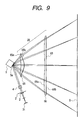
- Fig. 9 is a sectional view of the main part of an optical system in the main scanning direction showing one of a plurality of scanning optical devices constituting a color image forming apparatus according to the third embodiment of the present invention, and a corresponding photosensitive drum.
- the same reference numerals as in Fig. 3 denote the same parts.
- the third embodiment is different from the first embodiment in that a multi-semiconductor laser having a plurality of light-emitting portions (light-emitting points) is adopted as a light source means and that an imaging position deviation in the main scanning direction caused by the wavelength variation of the light source is compensated at high precision along with this change.
- the remaining arrangement and optical operation are almost the same as in the first embodiment, and provide the same effects.
- a light source means 31 is formed from a multi-semiconductor laser (multi-beam laser source) having a plurality of light-emitting portions (two in the third embodiment), and emits a plurality of beams (only one beam is shown in Fig. 9) modulated independently.
- multi-semiconductor laser multi-beam laser source
- a scanning optical element 26 as a third optical element (compensation means) having an f- ⁇ characteristic has a refraction element 65 and diffraction element 66.
- the refraction element 65 is formed from a single plastic toric lens having different powers in the main scanning direction and sub scanning direction. Two lens surfaces 65a and 65b of the toric lens 65 in the main scanning direction are aspherical.
- the diffraction element 66 is formed from an elongated composite optical element having different powers in the main scanning direction and sub scanning direction.
- An incident-side surface 66a of the composite optical element 66 is an aspherical surface having a predetermined power in only the main scanning direction (surface in the sub scanning direction is flat), whereas an exit-side surface 66b is a diffraction surface with a diffraction grating 83 added to a flat surface.
- two beams emitted by the light source means 31 pass through the same path as in the first embodiment, and simultaneously scan a surface 8 in the sub scanning direction at a predetermined interval.
- Table 3 shows the optical layout in the third embodiment, aspherical coefficients of the toric lens 65, and aspherical coefficients and phase terms of the composite optical element 66.
- the power layout of the plastic toric lens 65 and composite optical element 66 can be appropriately set to compensate for both an imaging position variation caused by the wavelength fluctuation of the multi-semiconductor laser 31 in the main scanning direction and a focus variation caused by the environmental fluctuation (particularly temperature elevation) of the device in the sub scanning direction.
- the third embodiment can also compensate for a scanning interval variation (jitter) in the main scanning direction on the photosensitive drum surface 8 caused by the wavelength difference between a plurality of light-emitting portions.
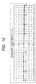
- Fig. 10 is a graph showing an imaging position variation in the main scanning direction caused by the wavelength variation of the multi-semiconductor laser 31 in the third embodiment.
- Fig. 10 shows a difference (5 nm) from the initial wavelength of the multi-semiconductor laser 31.
- Fig. 11 is a graph showing paraxial aberration (curvature of field in the main scanning direction and sub scanning direction) before and after an environmental fluctuation in the third embodiment.
- the solid line represents a characteristic (design value) before an environmental fluctuation, and the broken line represents a characteristic (effective value) when the temperature is elevated by 25°C.
- an imaging position deviation caused by a wavelength difference of +5 nm is 11 ⁇ m in the third embodiment, and corresponds to a pixel (position) deviation suppressed within about 1/4 pixel in, e.g., a printer having a resolution of 600 dpi.
- the initial wavelength deviation of the multi-semiconductor laser between a plurality of colors, the initial wavelength deviation between a plurality of light-emitting portions, or mode hopping in activation is permitted by about 5 nm.
- the focus movement amount in the sub scanning direction at a temperature elevated by 25°C is 0.2 mm, and is suppressed to a visually negligible level both in the sub scanning direction and main scanning direction.
- the third embodiment compensates for all these environmental fluctuations using a plastic optical element. This can simultaneously reduce the manufacturing cost by molding and shorten the optical path by large-field-angle aberration correction using an aspherical surface.
- the chromatic aberration of magnification (imaging position variation in the main scanning direction) caused by the wavelength fluctuation of the multi-semiconductor laser 31 is corrected at higher precision. Jitter caused by the wavelength difference between a plurality of light-emitting portions can also be reduced.
- the third embodiment uses the plastic toric lens 65 and composite optical element 66 as the scanning optical element 26 of the scanning optical device, and records images on a plurality of photosensitive drums by a plurality of scanning optical devices.
- a color image forming apparatus in which jitter in the use of the multi-semiconductor laser is suppressed, and misregistration between colors caused by a wavelength fluctuation or environmental fluctuation, and density nonuniformity between colors are reduced can be implemented with a simple arrangement at low cost.
- a focus position variation in the sub scanning direction on a surface to be scanned that is caused by the environmental fluctuation of the device is compensated by the power variation of the refraction element and diffraction element and the wavelength variation of the light source means.
- a focus position variation in the main scanning direction on a surface to be scanned that is caused by an environmental fluctuation is also compensated by the power variation of the refraction element and diffraction element and the wavelength variation of the light source means.
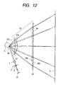
- Fig. 12 is a sectional view (sectional view of main scanning) of the main part of an optical system showing one of a plurality of scanning optical devices constituting a color image forming apparatus in the main scanning direction according to the fourth embodiment of the present invention, and a corresponding photosensitive drum.
- the same reference numerals as in Fig. 3 denote the same parts.
- the fourth embodiment is different from the first embodiment in that a multi-semiconductor laser (multi-beam laser source) having a plurality of light-emitting portions (light-emitting points) is adopted as a light source means, that the power ratio of the refraction element to diffraction element of a scanning optical element (third optical element) is appropriately set to compensate for an aberration variation along with an environmental fluctuation, and that an imaging position deviation caused by a wavelength variation not accompanied by any environmental fluctuation is set to a desired value or less.
- the remaining arrangement and optical action are almost the same as in the first embodiment, and provide the same effects.
- a scanning optical element 36 as a third optical element having an f- ⁇ characteristic has a refraction element 67 and diffraction element 68.
- the refraction element 67 is formed from a single plastic toric lens having different powers in the main scanning direction and sub scanning direction.
- Two lens surfaces 67a and 67b of the toric lens 67 in the main scanning direction are aspherical.
- the diffraction element 68 is formed from an elongated composite optical element having different powers in the main scanning direction and sub scanning direction.
- An incident-side surface 68a of the composite optical element 68 is an aspherical surface having a predetermined power in only the main scanning direction (surface in the sub scanning direction is flat), whereas an exit-side surface 68b is a diffraction surface with a diffraction grating 84 added to a flat surface.
- the power layout of the plastic toric lens 67 and composite optical element 68 is appropriately set.
- an imaging position deviation caused by a wavelength variation along with an environmental fluctuation, and an imaging position deviation caused by the refractive index variation of the material of the scanning optical element are set to opposite directions at the two ends of an effective image region (effective scanning region).
- an imaging position deviation caused by the refractive index variation of the material of the scanning optical element are set to opposite directions at the two ends of an effective image region (effective scanning region).
- an effective image region effective scanning region
- a focus variation caused by an environmental fluctuation is compensated.
- the environmental fluctuation means the temperature variation of the scanning optical device determined by self-temperature elevation in the scanning optical device, heat generation from another building component (fixing unit or the like) in the image forming apparatus, or an atmospheric variation at the installation location of the image forming apparatus.
- the chromatic aberration of magnification of the entire scanning optical element 36 is compensated by excessive correction in the main scanning direction by the refraction element 67 having a positive dispersion and the diffraction element 68 having a negative dispersion.
- the reason of slightly excessively correcting the chromatic aberration of magnification is to change a wavelength variation along with the above-mentioned environmental fluctuation and an imaging position variation in the main scanning direction caused by a refractive index variation to directions in which these variations cancel each other. This increases the refracting power in the scanning optical system, and enhances the aberration correction effect by the diffraction element.
- the power layout desirably satisfies ⁇ Lm/ ⁇ L + ⁇ Dm/ ⁇ D ⁇ 0
- the Abbe number has a limited range of values.
- the power ratio of the refraction element 67 to the diffraction element 68 in the main scanning direction desirably satisfies a condition: ⁇ L/(2 x 3.45) ⁇ ⁇ Lm/ ⁇ Dm ⁇ ⁇ L/3.45 ⁇ ⁇ L/6.90 ⁇ ⁇ Lm/ ⁇ Dm ⁇ ⁇ L/3.45
- the imaging position in the main scanning direction varies due to a variation such as the initial wavelength deviation of the multi-semiconductor laser not accompanied by any environmental fluctuation, a discrete wavelength variation by mode hopping, or the wavelength deviation between a plurality of light sources of the multi-semiconductor laser.
- a wavelength variation by mode hopping of the multi-semiconductor laser is a discrete variation with high visibility. For this reason, an imaging position variation in the main scanning direction per unit mode hopping must be set to 3 ⁇ m or less at the two ends of the effective image region.
- the fourth embodiment solves this problem by setting an imaging position variation in the main scanning direction per unit mode hopping of the multi-semiconductor laser to 3 ⁇ m or less at the two ends of the effective image region.
- the mode hopping means a shift of an optical output from a laser during single-mode oscillation from a given longitudinal mode to another longitudinal mode.
- Period mode hopping means "per wavelength variation” caused by a change to an adjacent mode.
- the refractive index variation of the scanning optical element caused by the environmental fluctuation (particularly temperature elevation) of the scanning optical device is compensated by the wavelength variation of the multi-semiconductor laser caused by a similar environmental fluctuation, thereby canceling focus movement (temperature compensation).
- the power layout is desirably set to 1.0 ⁇ ⁇ Ls/ ⁇ Ds ⁇ 2.6 where
- Table 4 shows the optical layout in the fourth embodiment, aspherical coefficients of the toric lens 67, and aspherical coefficients and phase terms of the composite optical element 68.
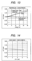
- Fig. 13 is a graph showing an imaging position deviation at the end of the effective image region (most off-axis beam) when the scanning optical device in the fourth embodiment is elevated from room temperature (design temperature).
- the dotted line represents a component generated upon a decrease in the refractive index of the material of the scanning optical element along with temperature elevation.
- the chain line represents a component generated upon the wavelength variation of the multi-semiconductor laser along with temperature elevation.
- the solid line represents an imaging position deviation caused by temperature elevation as the total of these components, both of which are deviation amounts from the design temperature.
- Fig. 14 is a graph showing an imaging position deviation as a function of a wavelength variation not accompanied by temperature elevation at the end of the effective image region (most off-axis beam). Fig. 14 shows a deviation amount from the reference wavelength.
- an imaging position deviation in the main scanning direction per unit mode hopping (0.3 nm in the multi-semiconductor laser of the fourth embodiment) is about 1.3 ⁇ m which is substantially negligible with respect to a discrete wavelength variation.
- Fig. 15 is a graph showing paraxial aberration (focus position in the main scanning direction and sub scanning direction) before and after an environmental fluctuation in the fourth embodiment.
- the solid line represents a characteristic (design value) before an environmental fluctuation, and the broken line represents a characteristic (effective value) when the temperature of the scanning optical device is elevated by 25°C.
- focus deviations in the main scanning direction and sub scanning direction caused by an environmental fluctuation must be suppressed to ⁇ 1.0 mm or less in order that misregistration between colors and image density nonuniformity between colors may be visually inconspicuous.
- the focus movement amount in the sub scanning direction at a temperature elevated by 25°C is 0.2 mm in the fourth embodiment, and is suppressed to a visually negligible level both in the sub scanning direction and main scanning direction.
- the fourth embodiment compensates for all these environmental fluctuations using a plastic optical element. This can simultaneously reduce the manufacturing cost by molding and shorten the optical path by large-field-angle aberration correction using an aspherical surface.
- the fourth embodiment appropriately sets the powers of the refraction element and diffraction element as the scanning optical element of the scanning optical device such that an imaging position deviation in the main scanning direction caused by a wavelength variation along with an environmental fluctuation, and an imaging position deviation caused by the refractive index variation of the material of the scanning optical element are set to opposite directions at the two ends of the effective image region, thereby reducing an imaging position deviation caused by an environmental fluctuation.
- an imaging position deviation caused by a wavelength variation not accompanied by any environmental fluctuation is also set to a desired value or less, thereby implementing a scanning optical device resistant to a wavelength fluctuation or environmental fluctuation.
- the fourth embodiment uses a plurality of scanning optical devices to record images on a plurality of photosensitive drum surfaces.
- a color image forming apparatus in which misregistration between colors caused by a wavelength fluctuation or environmental fluctuation, and density nonuniformity between colors are reduced can be implemented with a simple arrangement at low cost.
- the fourth embodiment has exemplified the use of a multi-beam laser source for a tandem type color image forming apparatus whose precision requirement is the highest.
- this embodiment is effective regardless of the type of scanning optical device such as a color/monochrome device or a single-beam laser source/multi-beam laser source.
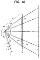
- Fig. 16 is a sectional view (sectional view of main scanning) of the main part of an optical system showing one of a plurality of scanning optical devices constituting a'color image forming apparatus in the main scanning direction according to the fifth embodiment of the present invention, and a corresponding photosensitive drum.
- the same reference numerals as in Fig. 12 denote the same parts.
- the fifth embodiment is different from the fourth embodiment in that a semiconductor laser (single-beam laser source) having a single light-emitting portion is used as a light source means, and that the power ratio of the refraction element to diffraction element of the scanning optical element is optimized.
- the remaining arrangement and optical action are almost the same as in the fourth embodiment, and provide the same effects.
- a scanning optical element 46 as a third optical element having an f- ⁇ characteristic has a refraction element 69 and diffraction element 70.
- the refraction element 69 is formed from a single plastic toric lens having different powers in the main scanning direction and sub scanning direction.
- Two lens surfaces 69a and 69b of the toric lens 69 in the main scanning direction are aspherical.
- the diffraction element 70 is formed from an elongated composite optical element having different powers in the main scanning direction and sub scanning direction.
- An incident-side surface 70a of the composite optical element 70 is an aspherical surface having a predetermined power in only the main scanning direction (surface in the sub scanning direction is flat), whereas an exit-side surface 70b is a diffraction surface with a diffraction grating 85 added to a flat surface.
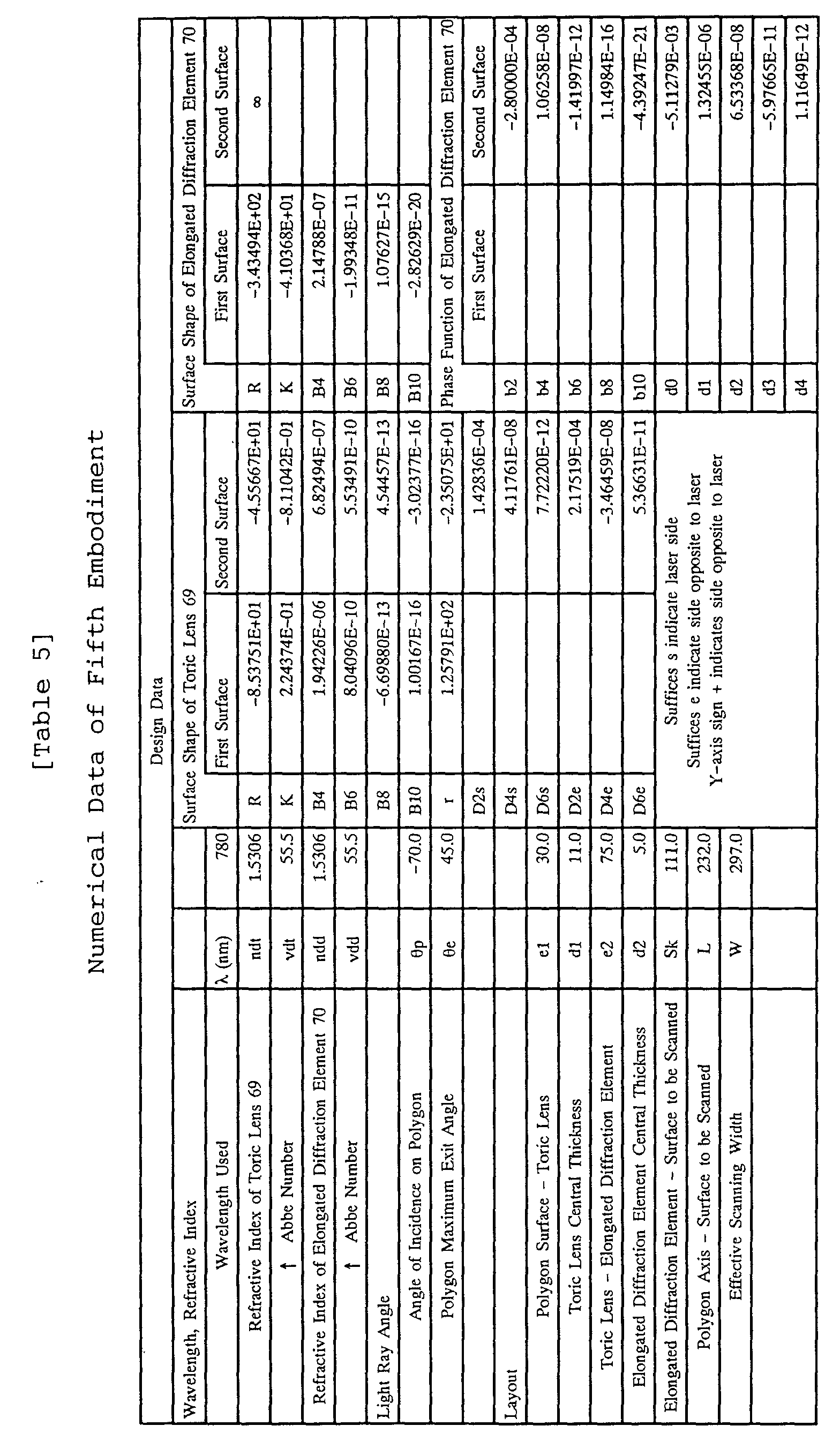
- Table 5 shows the optical layout in the fifth embodiment, aspherical coefficients of the toric lens 69, and aspherical coefficients and phase terms of the composite optical element 70.
- the power layout of the plastic toric lens 69 and composite optical element 70 is appropriately set.
- an imaging position variation caused by a wavelength variation along with an environmental fluctuation, and an imaging position deviation caused by the refractive index variation of the material of the scanning optical element are set to opposite directions at the two ends of the effective image region.
- a focus variation caused by an environmental fluctuation is compensated.
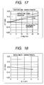
- Fig. 17 is a graph showing an imaging position deviation at the end of the effective image region (most off-axis beam) when the scanning optical device in the fifth embodiment is elevated from room temperature (design temperature).
- the dotted line represents a component generated upon a decrease in the refractive index of the material of the scanning optical element along with temperature elevation.
- the chain line represents a component generated upon the wavelength variation of the semiconductor laser along with temperature elevation.
- the solid line represents an imaging position deviation caused by temperature elevation as the total of these components, both of which are deviation amounts from the design temperature.
- the fifth embodiment relatively increases the power of the diffraction element, thereby increasing an imaging position deviation caused by the wavelength variation of the semiconductor laser along with temperature elevation, and enhancing the correction effect together with a component generated upon a decrease in the refractive index of the material of the scanning optical element.
- Fig. 18 is a graph showing an imaging position deviation as a function of a wavelength variation not accompanied by temperature elevation at the end of the effective image region (most off-axis beam). Fig. 18 shows a deviation amount from the reference wavelength.
- an imaging position deviation in the main scanning direction per unit mode hopping (0.3 nm in the semiconductor laser of the fifth embodiment) is about 2.0 ⁇ m which is substantially negligible with respect to a discrete wavelength variation.
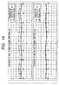
- Fig. 19 is a graph showing paraxial aberration (focus position in the main scanning direction and sub scanning direction) before and after an environmental fluctuation in the fifth embodiment.
- the solid line represents a characteristic (design value) before an environmental fluctuation, and the broken line represents a characteristic (effective value) when the temperature of the scanning optical device is elevated by 25°C.
- the focus movement amount in the sub scanning direction at a temperature elevated by 25°C is 0.2 mm in the fifth embodiment, and is suppressed to a visually negligible level both in the sub scanning direction and main scanning direction.
- the fifth embodiment appropriately sets the powers of the refraction element and diffraction element as the scanning optical element of the scanning optical device such that an imaging position deviation in the main scanning direction caused by a wavelength variation along with an environmental fluctuation, and an imaging position deviation caused by the refractive index variation of the material of the scanning optical element are set to opposite directions at the two ends of the effective image region, thereby reducing an imaging position deviation caused by an environmental fluctuation.
- an imaging position deviation caused by a wavelength variation not accompanied by any environmental fluctuation is also set to a desired value or less, thereby implementing a scanning optical device resistant to a wavelength variation or environmental variation.
- the power of the diffraction element is relatively increased to increase an imaging position deviation caused the wavelength variation of the semiconductor laser along with temperature elevation and to enhance the correction effect together with a component generated upon a decrease in the refractive index of the material of the scanning optical element.
- a scanning optical device more resistant to an environmental variation is implemented.
- the fifth embodiment uses a plurality of scanning optical devices to record images on a plurality of photosensitive drum surfaces.
- a color image forming apparatus in which misregistration between colors caused by a wavelength fluctuation or environmental fluctuation, and density nonuniformity between colors are reduced can be implemented with a simple arrangement at low cost.
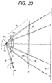
- Fig. 20 is a sectional view (sectional view of main scanning) of the main part of an optical system showing one of a plurality of scanning optical devices constituting a color image forming apparatus in the main scanning direction according to the sixth embodiment of the present invention, and a corresponding photosensitive drum.
- the same reference numerals as in Fig. 12 denote the same parts.
- the sixth embodiment is different from the fifth embodiment in that a plastic toric lens as a refraction element is made of a material such as polycarbonate (PC) having a large dispersion, and that the power ratio of the refraction element to the diffraction element is optimized.
- PC polycarbonate
- a scanning optical element 56 as a third optical element having an f- ⁇ characteristic has a refraction element 71 and diffraction element 72.
- the refraction element 71 is formed from a single plastic toric lens of a material such as polycarbonate (PC) having a large dispersion with different powers in the main scanning direction and sub scanning direction.
- Two lens surfaces 61a and 71b of the toric lens 71 in the main scanning direction are aspherical.
- the diffraction element 72 is formed from an elongated composite optical element having different powers in the main scanning direction and sub scanning direction.
- An incident-side surface 72a of the composite optical element 72 is an aspherical surface having a predetermined power in only the main scanning direction (surface in the sub scanning direction is flat), whereas an exit-side surface 72b is a diffraction surface with a diffraction grating 86 added to a flat surface.
- Table 6 shows the optical layout in the sixth embodiment, aspherical coefficients of the toric lens 71, and aspherical coefficients and phase terms of the composite optical element 72.
- the power layout of the plastic toric lens 71 and composite optical element 72 is appropriately set.
- an imaging position variation caused by a wavelength variation along with an environmental fluctuation, and an imaging position deviation caused by the refractive index variation of the material of the scanning optical element are set to opposite directions at the two ends of the effective image region.
- a focus variation caused by an environmental variation is compensated.
- the refraction element is made of a material such as PC having a large dispersion. Hence, the power of the diffraction element can be relatively increased, which is effective in aberration correction and enables high-precision aberration correction.
- Fig. 21 is a graph showing an imaging position deviation at the end of the effective image region (most off-axis beam) when the scanning optical device in the sixth embodiment is elevated from room temperature (design temperature).
- the dotted line represents a component generated upon a decrease in the refractive index of the material of the scanning optical element along with temperature elevation.
- the chain line represents a component generated upon the wavelength variation of the semiconductor laser along with temperature elevation.
- the solid line represents an imaging position deviation caused by temperature elevation as the total of these components, both of which are deviation amounts from the design temperature.
- Fig. 22 is a graph showing an imaging position deviation as a function of a wavelength variation not accompanied by temperature elevation at the end of the effective image region (most off-axis beam). Fig. 22 shows a deviation amount from the reference wavelength.
- an imaging position deviation in the main scanning direction per unit mode hopping (0.3 nm in the semiconductor laser of the sixth embodiment) is about 1.2 ⁇ m which is substantially negligible with respect to a discrete wavelength variation.
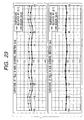
- Fig. 23 is a graph showing paraxial aberration (focus position in the main scanning direction and sub scanning direction) before and after an environmental fluctuation in the sixth embodiment.
- the solid line represents a characteristic (design value) before an environmental fluctuation, and the broken line represents a characteristic (effective value) when the temperature of the scanning optical device is elevated by 25°C.
- the focus movement amount in the sub scanning direction at a temperature elevated by 25°C is 0.2 mm in the sixth embodiment, and is suppressed to a visually negligible level both in the sub scanning direction and main scanning direction.
- the sixth embodiment appropriately sets the powers of the refraction element and diffraction element as the scanning optical element of the scanning optical device such that an imaging position deviation in the main scanning direction caused by a wavelength variation along with an environmental fluctuation, and an imaging position deviation caused by the refractive index variation of the material of the scanning optical element are set to opposite directions at the two ends of the effective image region, thereby reducing an imaging position deviation caused by an environmental variation.
- an imaging position deviation caused by a wavelength variation not accompanied by any environmental fluctuation is also set to a desired value or less, thereby implementing a scanning optical device resistant to a wavelength fluctuation or environmental fluctuation.
- this embodiment can use PC with a large dispersion to increase the power of the diffraction element, thus implementing a scanning optical device which corrects aberration at high precision.
- the sixth embodiment uses a plurality of scanning optical devices to record images on a plurality of photosensitive drum surfaces.
- a color image forming apparatus in which misregistration between colors caused by a wavelength fluctuation or environmental fluctuation, and density nonuniformity between colors are reduced can be implemented with a simple arrangement at low cost.
- Fig. 26 is a schematic view showing the main part of an image forming apparatus.
- This embodiment concerns a tandem type color image forming apparatus in which four scanning optical devices are aligned to record pieces of image information on photosensitive drum surfaces serving as image carriers in parallel with each other.
- a color image forming apparatus 160 comprises scanning optical devices 111, 112, 113, and 114 having any one of the arrangements described in the first to sixth embodiments, photosensitive drums 121, 122, 123, and 124 serving as image carriers, developing units 131, 132, 133, and 134, and a convey belt 151.
- the color image forming apparatus 160 receives R (Red), G (Green), and B (Blue) color signals from an external device 152 such as a personal computer. These color signals are converted into C (Cyan), M (Magenta), Y (Yellow), and B (Black) image data (dot data) by a printer controller 153 in the apparatus. These image data are respectively input to the scanning optical devices 111, 112, 113, and 114.
- the scanning optical devices emit beams 141, 142, 143, and 144 modulated in accordance with these image data.
- the beams scan the photosensitive surfaces of the photosensitive drums 121, 122, 123, and 124 in the main scanning direction.
- the four scanning optical devices (111, 112, 113, and 114) are aligned, respectively correspond to C (Cyan), M (Magenta), Y (Yellow), and B (Black) colors, and record image signals (image information) on the surfaces of the photosensitive drums 121, 122, 123, and 124 in parallel with each other, thereby printing a color image at a high speed.
- the four scanning optical devices 111, 112, 113, and 114 use beams based on their image data to form latent images of the respective colors on the surfaces of the corresponding photosensitive drums 121, 122, 123, and 124. After that, the latent images are multiple-transferred to a recording medium to form one full-color image.
- the external device 152 e.g., a color image reading device having a CCD sensor may be used.
- the color image reading device and the color image forming apparatus 160 constitute a color digital copying machine.
- the present invention can achieve a compact scanning optical device and color image forming apparatus suitable for high-resolution printing in which an imaging position variation caused by the wavelength variation of a light source means, an aberration variation upon an environmental variation (temperature variation), and the like in each scanning optical device are compensated by a compensation means (third optical element) in a color image forming apparatus having a plurality of scanning optical devices, thereby suppressing an imaging position deviation in especially the main scanning direction, and reducing a color deviation and image density nonuniformity at low cost with a simple arrangement.
- the present invention can achieve a scanning optical device and color image forming apparatus in which a refraction element and diffraction element are used as the scanning optical element of a scanning optical device, the powers of the refraction element and diffraction element are set such that an imaging position deviation in the main scanning direction caused by a wavelength variation along with the environmental fluctuation of the scanning optical device and an imaging position deviation caused by the refractive index variation of the material of the scanning optical element are set to opposite directions at the two ends of an effective image region (effective scanning region), thereby reducing an imaging position deviation caused by an environmental fluctuation, and at the same time an imaging position deviation caused by a wavelength variation not accompanied by any environmental fluctuation is also set to a desired value or less, thereby implementing a scanning optical device resistant to a wavelength fluctuation or environmental fluctuation, and in which images are recorded on a plurality of image carriers (photosensitive drums) using a plurality of scanning optical devices, thereby implementing with a simple arrangement at low cost a color image forming apparatus which is
Landscapes
- Physics & Mathematics (AREA)
- General Physics & Mathematics (AREA)
- Optics & Photonics (AREA)
- Geometry (AREA)
- Laser Beam Printer (AREA)
- Facsimile Scanning Arrangements (AREA)
- Mechanical Optical Scanning Systems (AREA)
- Lenses (AREA)
Abstract
Description
The image forming apparatus requires not only stable optical performance in one scanning optical device (single color) but also an arrangement which can prevent misregistration or image nonuniformity between colors even when the light source wavelength (wavelength of a beam emitted by the light source), initial wavelength, or use environment (particularly ambient temperature) of the scanning optical device fluctuates, or even when the light source wavelengths, initial wavelengths, or use environments of a plurality of scanning optical devices differ.
wherein powers of said refraction element and said diffraction element are set such that an imaging position deviation in a main scanning direction on a surface to be scanned that is caused by a wavelength variation of a beam emitted by said light source means along with an environmental fluctuation of said scanning optical device, and an imaging position deviation in the main scanning direction on the surface to be scanned that is caused by a refractive index variation of a material of said optical element along with an environmental fluctuation are set to be in opposite directions at two ends of an effective scanning region.
wherein said scanning optical device comprises compensation means having a refraction element and a diffraction element so as to compensate for an imaging position deviation in a main scanning direction on the surface to be scanned that is caused by a wavelength fluctuation of the beam emitted by said light source means, and
letting Lm and Dm be powers of said refraction element and said diffraction element in the main scanning direction, the powers satisfy a condition:
- Refraction surface ... aspherical shape whose main scanning direction can be represented by a function up to 10th order.
(where r0 is the sagittal radius of curvature on the optical axis, and D2, D4, D6, D8, and D10 are aspherical coefficients.)
- Diffraction surface ... diffraction surface whose
main scanning direction is represented by a function up
to 6th order and sub scanning direction is represented
by a 2nd-order phase function which changes depending
on the position of the main scanning direction, which
is represented by
- Ls:
- power of the refraction element in the sub scanning direction
- Ds:
- power of the diffraction element in the sub scanning direction


The refraction element 67 is formed from a single plastic toric lens having different powers in the main scanning direction and sub scanning direction. Two lens surfaces 67a and 67b of the toric lens 67 in the main scanning direction are aspherical.
- Ls:
- power of the refraction element in the sub scanning direction
- Ds:
- power of the diffraction element in the sub scanning direction


in which images are recorded on a plurality of image carriers (photosensitive drums) using a plurality of scanning optical devices, thereby implementing with a simple arrangement at low cost a color image forming apparatus which is almost free from misregistration between colors caused by a wavelength fluctuation or environmental fluctuation and almost free from density nonuniformity between colors.
Claims (12)
- A scanning optical device including light source means, and an optical element having a refraction element and a diffraction element,
characterized in that powers of said refraction element and said diffraction element are set such that an imaging position deviation in a main scanning direction on a surface to be scanned that is caused by a wavelength variation of a beam emitted by said light source means along with an environmental fluctuation of said scanning optical device, and an imaging position deviation in the main scanning direction on the surface to be scanned that is caused by a refractive index variation of a material of said optical element along with an environmental fluctuation are set to be in opposite directions at two ends of an effective scanning region. - A device according to claim 1, characterized in that said optical element includes an element which forms the beam emitted by said light source means into an image on the surface to be scanned, and letting Lm and Dm be powers of said refraction element and diffraction element constituting said optical element in the main scanning direction, and νL be an Abbe number of a material of said refraction element, the powers satisfy a condition:
- A device according to claim 2, characterized in that an imaging position variation per unit mode hopping of said light source means is not more than 3 µm at the two ends of the effective scanning region.
- A device according to claim 1 or 2, characterized in that a focus position deviation in a sub scanning direction on the surface to be scanned that is caused by the wavelength variation of the beam emitted by said light source means along with the environmental fluctuation, and a focus position deviation in the sub scanning direction on the surface to be scanned that is caused by the refractive index variation of the material of said optical element along with the environmental fluctuation are substantially compensated within the effective scanning region.
- A device according to any one of claims 1 to 3, characterized in that the environmental fluctuation includes an atmospheric variation of said scanning optical device and a temperature variation caused by self-temperature elevation.
- A device according to any one of claims 1 to 4, characterized in that said refraction element includes a toric lens, and said diffraction element includes a composite optical element obtained by integrating a refraction surface and a diffraction surface.
- A device according to any one of claims 1 to 5, characterized in that said refraction element and diffraction element constituting said optical element are formed from a plastic material.
- A device according to any one of claims 1 to 6, characterized in that said light source means includes a multi-beam laser source having a plurality of light-emitting portions.
- A device according to any one of claims 1 to 8, characterized in that letting Ls and Ds be powers of said refraction element and diffraction element constituting said optical element in a sub scanning direction, the powers satisfy a condition:
- A device according to any one of claims 1 to 9, characterized in that the powers of said refraction element and said diffraction element are set to compensate for an imaging position variation in the main scanning direction on the surface to be scanned that is caused by a wavelength fluctuation of the beam emitted by said light source means.
- An image forming apparatus characterized in that said image forming apparatus comprises a plurality of pairs of scanning optical devices defined in any one of claims 1 to 10 and corresponding image carriers, guides beams emitted by said scanning optical devices to corresponding image carriers, scans surfaces of said image carriers to form images of different colors on the surfaces of said image carriers, and forms a color image by the images formed on the surfaces of said image carriers.
- An image forming apparatus characterized by comprising a scanning optical device defined in any one of claims 1 to 10, and a printer controller for converting code data input from an external device into an image signal and inputting the converted image signal to said scanning optical device.
Applications Claiming Priority (2)
| Application Number | Priority Date | Filing Date | Title |
|---|---|---|---|
| JP2000020074 | 2000-01-28 | ||
| JP2000020074A JP2000292718A (en) | 1999-02-02 | 2000-01-28 | Scanning optical device and color image forming apparatus |
Publications (3)
| Publication Number | Publication Date |
|---|---|
| EP1122579A2 true EP1122579A2 (en) | 2001-08-08 |
| EP1122579A3 EP1122579A3 (en) | 2003-10-01 |
| EP1122579B1 EP1122579B1 (en) | 2007-10-03 |
Family
ID=18546691
Family Applications (1)
| Application Number | Title | Priority Date | Filing Date |
|---|---|---|---|
| EP01101721A Expired - Lifetime EP1122579B1 (en) | 2000-01-28 | 2001-01-25 | Scanning optical device and image forming apparatus |
Country Status (3)
| Country | Link |
|---|---|
| US (2) | US6643043B2 (en) |
| EP (1) | EP1122579B1 (en) |
| DE (1) | DE60130694T2 (en) |
Cited By (3)
| Publication number | Priority date | Publication date | Assignee | Title |
|---|---|---|---|---|
| EP1391771A3 (en) * | 2002-08-08 | 2004-06-16 | Canon Kabushiki Kaisha | Optical scanning device and image forming apparatus using the same |
| US7145591B2 (en) * | 2003-03-31 | 2006-12-05 | Canon Kabushiki Kaisha | Multi-beam optical scanning device |
| EP1667420B1 (en) * | 2001-03-05 | 2010-05-19 | Canon Kabushiki Kaisha | Image reading imaging optical system and image reading apparatus using the same |
Families Citing this family (8)
| Publication number | Priority date | Publication date | Assignee | Title |
|---|---|---|---|---|
| JP2000338435A (en) * | 1999-05-25 | 2000-12-08 | Canon Inc | Scanning optical device and image forming apparatus |
| KR100565051B1 (en) * | 2002-09-16 | 2006-03-30 | 삼성전자주식회사 | Optical scanning unit and electrophotographic image forming apparatus employing the same |
| US7411712B2 (en) * | 2003-03-19 | 2008-08-12 | Ricoh Company, Limited | Optical scanner and image formation apparatus |
| WO2005106566A1 (en) * | 2004-04-30 | 2005-11-10 | Nalux Co., Ltd. | Beam shaping optical system and optical system of laser beam printer |
| US7136208B2 (en) * | 2004-11-01 | 2006-11-14 | Canon Kabushiki Kaisha | Light scanning apparatus and image forming apparatus using the same |
| JP5024928B2 (en) * | 2006-09-04 | 2012-09-12 | 株式会社リコー | Optical scanning apparatus and image forming apparatus |
| US7688491B2 (en) * | 2006-09-15 | 2010-03-30 | Ricoh Company, Ltd. | Diffractive-optical element, scanning optical system, optical scanner, and image forming apparatus |
| JP2009122327A (en) * | 2007-11-14 | 2009-06-04 | Canon Inc | Multi-beam optical scanning device and image forming apparatus using the same |
Family Cites Families (14)
| Publication number | Priority date | Publication date | Assignee | Title |
|---|---|---|---|---|
| JP2623147B2 (en) | 1990-02-07 | 1997-06-25 | キヤノン株式会社 | Optical system for light beam scanning |
| US5179465A (en) | 1990-02-07 | 1993-01-12 | Canon Kabushiki Kaisha | Optical system for light beam scanning |
| JP2850724B2 (en) | 1993-11-02 | 1999-01-27 | 富士ゼロックス株式会社 | Color image forming equipment |
| US5691847A (en) * | 1994-08-08 | 1997-11-25 | Hughes Aircraft Company | Athermalized and achromatized optical systems employing diffractive optical element |
| JP3231218B2 (en) | 1995-06-13 | 2001-11-19 | 東光電気株式会社 | Arc extinguishing cover for high pressure air switch |
| US5838480A (en) * | 1996-04-29 | 1998-11-17 | The University Of Rochester | Optical scanning system with diffractive optics |
| JP3432085B2 (en) * | 1996-08-28 | 2003-07-28 | キヤノン株式会社 | Scanning optical device |
| JP3397624B2 (en) | 1996-12-19 | 2003-04-21 | キヤノン株式会社 | Scanning optical device and laser beam printer having the same |
| JP3535686B2 (en) * | 1997-03-03 | 2004-06-07 | 株式会社リコー | Multi-beam laser scanner |
| US6067106A (en) | 1997-04-16 | 2000-05-23 | Canon Kabushiki Kaisha | Scanning optical apparatus |
| US6115164A (en) * | 1997-07-22 | 2000-09-05 | Asahi Kogaku Kogyo Kabushiki Kaisha | Scanning optical system |
| JPH1144854A (en) * | 1997-07-24 | 1999-02-16 | Canon Inc | Optical scanning optical device |
| JPH11223783A (en) * | 1998-02-04 | 1999-08-17 | Canon Inc | Color image forming equipment |
| US6038053A (en) * | 1998-02-04 | 2000-03-14 | Canon Kabushiki Kaisha | Color image forming apparatus |
-
2001
- 2001-01-25 US US09/768,498 patent/US6643043B2/en not_active Expired - Lifetime
- 2001-01-25 EP EP01101721A patent/EP1122579B1/en not_active Expired - Lifetime
- 2001-01-25 DE DE60130694T patent/DE60130694T2/en not_active Expired - Lifetime
-
2003
- 2003-04-03 US US10/405,218 patent/US6816293B2/en not_active Expired - Lifetime
Cited By (6)
| Publication number | Priority date | Publication date | Assignee | Title |
|---|---|---|---|---|
| EP1667420B1 (en) * | 2001-03-05 | 2010-05-19 | Canon Kabushiki Kaisha | Image reading imaging optical system and image reading apparatus using the same |
| EP1391771A3 (en) * | 2002-08-08 | 2004-06-16 | Canon Kabushiki Kaisha | Optical scanning device and image forming apparatus using the same |
| US7034859B2 (en) | 2002-08-08 | 2006-04-25 | Canon Kabushiki Kaisha | Optical scanning device and image forming apparatus using the same |
| US7248279B2 (en) | 2002-08-08 | 2007-07-24 | Canon Kabushiki Kaisha | Optical scanning device and image forming apparatus using the same |
| US7145591B2 (en) * | 2003-03-31 | 2006-12-05 | Canon Kabushiki Kaisha | Multi-beam optical scanning device |
| US7598974B2 (en) | 2003-03-31 | 2009-10-06 | Canon Kabushiki Kaisha | Multi-beam optical scanning device |
Also Published As
| Publication number | Publication date |
|---|---|
| US20010035943A1 (en) | 2001-11-01 |
| US6643043B2 (en) | 2003-11-04 |
| DE60130694D1 (en) | 2007-11-15 |
| EP1122579B1 (en) | 2007-10-03 |
| US20030202230A1 (en) | 2003-10-30 |
| DE60130694T2 (en) | 2008-07-17 |
| EP1122579A3 (en) | 2003-10-01 |
| US6816293B2 (en) | 2004-11-09 |
Similar Documents
| Publication | Publication Date | Title |
|---|---|---|
| EP0872754B1 (en) | Scanning optical apparatus with a diffractive lens for compensating temperature dependent focus changes | |
| US7362486B2 (en) | Optical scanning device with at least one resin lens for controlling a beam waist position shift | |
| EP0827004A2 (en) | Corrected scanning optical apparatus | |
| US6038053A (en) | Color image forming apparatus | |
| US7586661B2 (en) | Optical scanning device and image forming apparatus | |
| US8390908B2 (en) | Optical scanning apparatus, and image forming apparatus | |
| JP2008076557A (en) | Optical scanning device and image forming apparatus using the same | |
| KR100854024B1 (en) | Optical scanning device and method of adjusting the optical scanning device | |
| JP4015249B2 (en) | Multi-beam exposure system | |
| US7554709B2 (en) | Optical scanning apparatus and image forming apparatus employing this apparatus | |
| US7126625B2 (en) | Optical scanning device and image forming apparatus using the same | |
| US6816293B2 (en) | Scanning optical device and image forming apparatus | |
| JP2004070107A (en) | Optical scanning device and image forming apparatus using the same | |
| JP4508458B2 (en) | Optical scanning device and image forming apparatus using the same | |
| JPH11223783A (en) | Color image forming equipment | |
| JP4455309B2 (en) | Optical scanning device and image forming apparatus using the same | |
| JP2000292718A (en) | Scanning optical device and color image forming apparatus | |
| JP2005215188A (en) | Scanning optical device | |
| JPH11223784A (en) | Color image forming equipment | |
| JP7581103B2 (en) | Optical scanning device and image forming device | |
| JP4902279B2 (en) | Image forming apparatus | |
| JP2002333591A (en) | Scanning optical device and color image forming apparatus having the same | |
| JP2001142020A (en) | Tandem scanning optical device | |
| JPH11237568A (en) | Exposure equipment | |
| JP2013246200A (en) | Light guide optical system, manufacturing method of the same, and optical scanner, and image forming apparatus |
Legal Events
| Date | Code | Title | Description |
|---|---|---|---|
| PUAI | Public reference made under article 153(3) epc to a published international application that has entered the european phase |
Free format text: ORIGINAL CODE: 0009012 |
|
| AK | Designated contracting states |
Kind code of ref document: A2 Designated state(s): AT BE CH CY DE DK ES FI FR GB GR IE IT LI LU MC NL PT SE TR |
|
| AX | Request for extension of the european patent |
Free format text: AL;LT;LV;MK;RO;SI |
|
| RIC1 | Information provided on ipc code assigned before grant |
Free format text: 7G 02B 26/10 A |
|
| PUAL | Search report despatched |
Free format text: ORIGINAL CODE: 0009013 |
|
| AK | Designated contracting states |
Kind code of ref document: A3 Designated state(s): AT BE CH CY DE DK ES FI FR GB GR IE IT LI LU MC NL PT SE TR |
|
| AX | Request for extension of the european patent |
Extension state: AL LT LV MK RO SI |
|
| RIC1 | Information provided on ipc code assigned before grant |
Ipc: 7G 02B 26/12 B Ipc: 7G 02B 26/10 A Ipc: 7G 02B 27/00 B |
|
| 17P | Request for examination filed |
Effective date: 20040220 |
|
| AKX | Designation fees paid |
Designated state(s): DE FR GB IT NL |
|
| 17Q | First examination report despatched |
Effective date: 20040924 |
|
| GRAP | Despatch of communication of intention to grant a patent |
Free format text: ORIGINAL CODE: EPIDOSNIGR1 |
|
| GRAS | Grant fee paid |
Free format text: ORIGINAL CODE: EPIDOSNIGR3 |
|
| GRAA | (expected) grant |
Free format text: ORIGINAL CODE: 0009210 |
|
| AK | Designated contracting states |
Kind code of ref document: B1 Designated state(s): DE FR GB IT NL |
|
| REG | Reference to a national code |
Ref country code: GB Ref legal event code: FG4D |
|
| REF | Corresponds to: |
Ref document number: 60130694 Country of ref document: DE Date of ref document: 20071115 Kind code of ref document: P |
|
| ET | Fr: translation filed | ||
| PLBE | No opposition filed within time limit |
Free format text: ORIGINAL CODE: 0009261 |
|
| STAA | Information on the status of an ep patent application or granted ep patent |
Free format text: STATUS: NO OPPOSITION FILED WITHIN TIME LIMIT |
|
| 26N | No opposition filed |
Effective date: 20080704 |
|
| REG | Reference to a national code |
Ref country code: FR Ref legal event code: PLFP Year of fee payment: 16 |
|
| REG | Reference to a national code |
Ref country code: FR Ref legal event code: PLFP Year of fee payment: 17 |
|
| PGFP | Annual fee paid to national office [announced via postgrant information from national office to epo] |
Ref country code: NL Payment date: 20161205 Year of fee payment: 17 |
|
| PGFP | Annual fee paid to national office [announced via postgrant information from national office to epo] |
Ref country code: DE Payment date: 20170131 Year of fee payment: 17 Ref country code: FR Payment date: 20170126 Year of fee payment: 17 |
|
| PGFP | Annual fee paid to national office [announced via postgrant information from national office to epo] |
Ref country code: GB Payment date: 20170130 Year of fee payment: 17 |
|
| PGFP | Annual fee paid to national office [announced via postgrant information from national office to epo] |
Ref country code: IT Payment date: 20170209 Year of fee payment: 17 |
|
| REG | Reference to a national code |
Ref country code: DE Ref legal event code: R119 Ref document number: 60130694 Country of ref document: DE |
|
| REG | Reference to a national code |
Ref country code: NL Ref legal event code: MM Effective date: 20180201 |
|
| GBPC | Gb: european patent ceased through non-payment of renewal fee |
Effective date: 20180125 |
|
| PG25 | Lapsed in a contracting state [announced via postgrant information from national office to epo] |
Ref country code: FR Free format text: LAPSE BECAUSE OF NON-PAYMENT OF DUE FEES Effective date: 20180131 Ref country code: DE Free format text: LAPSE BECAUSE OF NON-PAYMENT OF DUE FEES Effective date: 20180801 |
|
| REG | Reference to a national code |
Ref country code: FR Ref legal event code: ST Effective date: 20180928 |
|
| PG25 | Lapsed in a contracting state [announced via postgrant information from national office to epo] |
Ref country code: GB Free format text: LAPSE BECAUSE OF NON-PAYMENT OF DUE FEES Effective date: 20180125 Ref country code: NL Free format text: LAPSE BECAUSE OF NON-PAYMENT OF DUE FEES Effective date: 20180201 |
|
| PG25 | Lapsed in a contracting state [announced via postgrant information from national office to epo] |
Ref country code: IT Free format text: LAPSE BECAUSE OF NON-PAYMENT OF DUE FEES Effective date: 20180125 |