EP1121053B1 - Protective enclosure for a fingerprint sensor - Google Patents
Protective enclosure for a fingerprint sensor Download PDFInfo
- Publication number
- EP1121053B1 EP1121053B1 EP99953102A EP99953102A EP1121053B1 EP 1121053 B1 EP1121053 B1 EP 1121053B1 EP 99953102 A EP99953102 A EP 99953102A EP 99953102 A EP99953102 A EP 99953102A EP 1121053 B1 EP1121053 B1 EP 1121053B1
- Authority
- EP
- European Patent Office
- Prior art keywords
- access piece
- sensor
- enclosure
- finger
- access
- Prior art date
- Legal status (The legal status is an assumption and is not a legal conclusion. Google has not performed a legal analysis and makes no representation as to the accuracy of the status listed.)
- Expired - Lifetime
Links
Images




Classifications
-
- A—HUMAN NECESSITIES
- A61—MEDICAL OR VETERINARY SCIENCE; HYGIENE
- A61B—DIAGNOSIS; SURGERY; IDENTIFICATION
- A61B5/00—Measuring for diagnostic purposes; Identification of persons
- A61B5/117—Identification of persons
- A61B5/1171—Identification of persons based on the shapes or appearances of their bodies or parts thereof
- A61B5/1172—Identification of persons based on the shapes or appearances of their bodies or parts thereof using fingerprinting
-
- G—PHYSICS
- G06—COMPUTING OR CALCULATING; COUNTING
- G06V—IMAGE OR VIDEO RECOGNITION OR UNDERSTANDING
- G06V40/00—Recognition of biometric, human-related or animal-related patterns in image or video data
- G06V40/10—Human or animal bodies, e.g. vehicle occupants or pedestrians; Body parts, e.g. hands
- G06V40/12—Fingerprints or palmprints
- G06V40/13—Sensors therefor
- G06V40/1306—Sensors therefor non-optical, e.g. ultrasonic or capacitive sensing
-
- G—PHYSICS
- G06—COMPUTING OR CALCULATING; COUNTING
- G06V—IMAGE OR VIDEO RECOGNITION OR UNDERSTANDING
- G06V40/00—Recognition of biometric, human-related or animal-related patterns in image or video data
- G06V40/10—Human or animal bodies, e.g. vehicle occupants or pedestrians; Body parts, e.g. hands
- G06V40/12—Fingerprints or palmprints
- G06V40/1335—Combining adjacent partial images (e.g. slices) to create a composite input or reference pattern; Tracking a sweeping finger movement
Definitions
- the present invention relates to enclosures for sensor devices, and more particularly to a protective enclosure which aligns an object placed on a biometric sensor.
- Biometric-oriented personal identification techniques are becoming increasingly important in protecting personal property, such as laptop computers and cellular phones, preventing credit card and calling card fraud, limiting access to security areas, computers and information, and ensuring security for electronic commerce.
- Biometric identification techniques use physical traits, measurements and characteristics specific to an individual. These characteristics include, but are not limited to, voice prints, hand prints, fingerprints, retina patterns, and signatures.
- biometric identification and verification techniques compare an individual's stored biometric data (the enrolled data) against newly obtained biometric data when the individual desires use of a protected item, access to a protected area or access to protected information. Due to its inherent nature, biometric data has the advantage of always being available for user identification and verification.
- the fingerprint biometric is one of the most widely used and researched biometric identification techniques.
- Existing technology allows the relevant features of a fingerprint to be represented in a few hundred bytes of data.
- the computer hardware required for recording and comparing fingerprint data can be centralized and accessed through a telecommunications network, centralized databases and processing hardware, with the result that costs may be amortized across many more transactions than would be the case for distributed processing.
- British Patent Number GB 1,267,996 discloses a system for identifying an individual by forming data sets containing the dimensions of an individual's fingers.
- Document US-A-3 804 524 describes an apparatus for directing and positioning a finger for print identification comprising the features of the preamble of claim 1.
- biometric sensors are susceptible to damage from impacts.
- solid-state biometric sensors are susceptible to damage from electrostatic discharge.
- the sensor may be particularly susceptible to electrostatic discharge, because the user touches the sensor during the sensing operation.
- a device for protecting the sensor from impacts, from electrostatic discharge and from other potentially harmful foreign materials, such as dust, dirt, sunlight and liquids.
- the present invention increases accuracy and reliability of biometric identification and verification techniques while protecting a sensor from harmful impacts and electrostatic discharge.
- Such protection and increased accuracy and reliability an achieved by providing an enclosure comprising a movable access piece made from a conductive material.
- the walls of the enclosure, together with the access piece cause the user to properly align a finger with the sensor.
- Protection from electrostatic discharge is achieved by grounding the access piece, which the user must move to reveal the sensor.
- the access piece is closed, protecting the sensor from harmful impacts.
- the present invention encloses a biometric sensor for sensing fingerprints.
- the sensor is mounted relative to an access piece, and the access piece is positionable between a closed position and at least one open position, preferably slidable, to reveal the sensor.
- the access piece is completely enclosed.
- the user slides the access piece to an open position using the finger he wishes to place on the sensor.
- the desired portion of the fingerprint is aligned with the sensor.
- the access piece is made from a conductive material, and it is electrically grounded. Since the user must touch the access piece to reveal the sensor, the user is electrostatically discharged before accessing the sensor.
- the present invention provides an apparatus for enclosing a biometric sensor.
- An enclosure according to the invention protects the sensor from harmful impacts, from electrostatic discharges (ESDs) and from other harmful material and electromagnetic energy.
- the enclosure protects a biometric sensor used for sensing fingerprints, and the enclosure is configured to cause a user to align the fingerprint core with the sensor during an access procedure.
- the enclosure of the invention is also used during enrollment.
- a method is provided for enrolling and reconstructing a fingerprint image which increases the likelihood of image overlap during an access procedure is described. Also, it is described an apparatus for indicating to the user when a fingerprint image of adequate quality is captured.
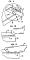
- FIG. 1A The preferred embodiment of the enclosure according to the invention is shown in FIG. 1A.
- the enclosure 100 comprises an access piece 110 which is shown in the closed position.
- the access piece 110 is a sliding door, and is movable in the direction of the arrows 112 and 114.
- a cross-section of the enclosure 100 with the access piece 110 in a closed position is shown in FIG. 1B.
- a sensor 130 is mounted in the enclosure 100 such that the closed access piece 110 covers the sensor 130, thereby protecting it from impacts.
- An exemplary embodiment of a fingerprint sensor device 130 that can be used in conjunction. with the present invention is explained in U.S Patent Application for a "Capacitive Fingerprint Sensor With Adjustable Gain,” filed May 13, 1997, which is now U.S. Patent No.
- the apparatus includes a planar array of capacitive sense elements disposed on a substrate. It also includes an insulating and receiving surface disposed over the array of sense elements, which is adapted to receive a finger so that a sense element and a portion of the finger surface located thereabove create a measurable change in capacitance.
- the capacitance is measured by first pre-charging each sense element, and then using a known current source to remove a fixed amount of charge from each capacitor plate. After a fingerprint is acquired, the quality of the fingerprint is evaluated, and if necessary, a gain parameter for the sense elements is iteratively adjusted until a satisfactory fingerprint is acquired.
- FIG. 1A Operation of the enclosure 100 is described with reference to FIG. 1A.
- FIG. 1B and FIG. 1C A user accesses the sensor 130 by placing a finger 120 on the access piece 110 and moving it in the direction of the arrow 112. In this position, the sensor 130 is fully revealed, as shown in FIG. 1C, and the finger 120 has access to the sensor 130. The finger 120 will then be disposed on the sensor 130 in a proper position and the sensing operation may proceed.
- a spring attaches the access piece 110 to the enclosure 100 such that the access piece 110 closes (is returned to the closed position) when the user releases the access piece 110.
- the access piece 110 is made of a conductive material and is electrically grounded.
- the access piece 110 When a user touches the access piece 110 to access the sensor 130, the user is grounded through the access piece 110. Because The finger 120 must continue to apply pressure to the access piece 110 to overcome the force of the spring, the finger 120 remains grounded throughout the sensing operation. Once the user releases the access piece 110, it automatically closes, thereby enclosing the sensor 130.
- the spring 180 is a coil spring with elongated ends, each end having a hook. At one end, the spring 180 is hooked to a coupling protrusion 181 on the access piece 110. The other end is hooked to the enclosure 100 at an aperture 183.
- the spring 180 When the spring 180 is relaxed (that is, not under tension), the access piece 110 is closed. To open the access piece 110, the user must overcome the force of the spring 180. Upou release, the spring 180 returns the access piece 110 to the closed position.
- the enclosure further comprises means for mechanically fastening the enclosure 100 to some other device, such as a laptop computer.
- the fastening means include a locating pin 187 and fastening toles 185 and 189.
- the locating pin 187 fits in a corresponding hole in the device of interest to locale the enclosure 100 in the desired position.
- Fastening holes 185 and 189 are configured to accept a corresponding fastening means, such as a screw.
- a switch 160 attached to the enclosure 100 is also provided.
- the switch 160 is operable to switch power to the sensor on and off.
- the switch 160 is positioned relative to the access piece 110 so that the access piece 110 engages the switch when the user slides the access piece 110 to access the sensor (not shown).
- the spring 180 causes the access piece 110 to return to the closed position. After the movement to the closed position, the access piece 110 disengages the switch 160 thereby turning off power to the sensor (not shown).
- the access piece 110 is configured to stop in a position which aligns the finger 120 with the sensor 130.
- the access piece 110 is shaped to form a fingertip contour 113.
- the user intuitively touches the access piece 110 in this contoured area 113 with the finger tip, because the fingertip naturally fits into the area 113.
- FIG. 1C when the access piece 110 is moved to an open position with the fingertip placed in the contoured area 113, the top of the finger 120 extends beyond the sensor 130 and the fingerprint core is aligned with the sensor 130.
- the enclosure 100 comprises guides 122 and 124 spaced apart by a predetermined width, preferably the width of the finger 120.
- the guides 122 and 124 are molded plastic walls. To accommodate fingers of various sizes, the walls may also be slanted inwardly from top to bottom; that is, toward the sensor.
- the guides laterally align the finger 120 on the sensor 130.
- the alignment provided by the access piece 110 in the open position and by the guides 122 and 124 enhances accuracy and reliability in acquiring the fingerprint image by minimizing finger placement error.
- the access piece may be configured in various ways to protect sensors designed for various uses.
- a side view of an enclosure 200 comprising a hinged 202, 204 and 206 access piece 210 is shown.
- the access piece 210 is made from a conductive material, and it is positionable at a closed position 212 and an open position 214. In the closed position 212, a sensor 220 is covered, protecting it 220 from impacts.
- the user pushes the piece 210 with his finger to the open position 214.
- the same previously described alignment and grounding features may be provided.
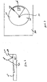
- the enclosure 300 comprises a rotatable access piece 310 which is positionable at a closed position 312 and at an open position 314.
- the user operates the access piece 310 by rotating it with his finger about a pivot 311 to the open position 314.
- the sensor 316 is revealed when the access piece 310 is at the open position 314.
- the access piece 310 is electrically conductive to ground, and is configured to return to the closed position when the user releases the access piece 310.
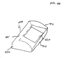
- An enclosure 400 comprises a housing 410 with an access end 412 and a closed end 414.
- the housing 410 protects a sensor 420 from impacts when the sensor 420 is not in use.
- An access piece 430 covers the access end 412.
- the access piece 430 is made from a conductive material and is swingable between a closed position (not shown) and an open position. The user accesses the sensor 420 by pushing on the access piece 430 with his finger.
- the access piece 430 is grounded, thereby protecting the sensor 420 from ESD.
- the housing 410 is shaped such that a finger placed within the housing is laterally aligned with the sensor 420.
- the closed end 414 of the housing 410 acts as a stop, causing the user to align his finger with the sensor 420 such that the core of the fingerprint is on the sensor 420.
- FIG. 4B A perspective of this configuration is shown in FIG. 4B.
- Walls 413 and 415 laterally constrain the finger (not shown) such that the finger is laterally aligned on the sensor 420.
- the closed end 414 acts as a constraint causing the fingerprint core to locate on the sensor 414.
- the access piece 430 is grounded to protect the sensor 420 from electrostatic discharge.
- the senor is mounted in a slidable unit.
- the enclosure 800 comprises a sliding unit 810.
- the sliding unit 810 In the closed position, the sliding unit 810 resides within the enclosure 800 and the sensor 820 is protected.
- An access piece 812 which is a button in this configuration, is operable to cause the sliding unit 810 to slide out of the enclosure 800.
- the means for sliding the sliding unit 810 into and out of the enclosure 800 may be a spring or motor.
- the button 812 is electrically conductive to a ground. The user is grounded when he presses the button 812 to release the sliding unit 810.
- An enclosure edge 817 constrains the finger in one direction and sliding unit edges 819 and 821 constrain the finger in a second and third direction.
- An enclosure is also described with an access piece positionable at a plurality of positions.
- an enclosure 500 is shown with an access piece 510 in a closed position, completely covering the sensor (not shown).
- the enclosure also comprises a stopper 530 which is operable to stop the access piece 510 at an open position.
- An arrow 535 marks a position on the enclosure 500, and a "1" and a "2,” or other such alignment marks, mark two positions on the access piece 510.
- the access piece 510 is positionable at multiple predetermined positions.
- FIG. 5B the enclosure 500 is shown with the access piece 510 positioned at position "1.” Only the tip of the finger 540 extends beyond the sensor 520, and the finger 540 and sensor 520 are positioned such that the top of the fingerprint image may be captured.
- FIG. 5C shows the relative positions of the sensor 520, access piece 510 and finger 540 when the access piece 510 is at position "2.” The finger 540 is positioned such that the fingerprint core is centered on the sensor 520, permitting capture of this portion of the fingerprint.
- FIG. 5D the access piece 510 is pushed to the stopper 530, and the finger 540 and sensor 520 are positioned such that an image of the bottom of the fingerprint may be captured.
- This procedure enables enrollment and reconstruction of a fingerprint image which comprises the combination of the images captured in position "1," position "2," and at the stop 530 position.
- This reconstructed image is known as a virtual image.
- This virtual image is advantageously larger than the sensor area.
- the virtual image 600 of FIG. 6 was captured and reconstructed according to the just-described procedure. As can be seen, the virtual image 600 is the combination of three overlapping images 611, 612 and 613 each of which is the size of the sensor.
- the resulting image 600 has a larger area than the sensor.
- alignment errors are overcome by the relatively larger area of the virtual image 600.
- the described apparatus and method increases the probability that the portion of the fingerprint placed on the sensor during an access procedure overlaps the enrolled image 600.
- a method for providing an image quality indicator is described with reference to the flow chart 700 of FIG 7.
- the finger is placed on a sensor enclosed with the previously described apparatus.
- the fingerprint image is captured.
- the quality of the image is evaluated in a decision step 730, and it is determined whether the image quality is adequate. If the image is adequate, the user is advised in a process step 740 that the image has been captured. When the image is inadequate, control returns to the process step 720 and the procedure is repeated.
- the image quality may be measured in many ways. For instance, contrast is one known attribute commonly used for evaluating an image; the image is evaluated by how well the intensity range of the image stretches over the maximum intensity range available. Image evaluation is described in W.K. Pratt, "Digital Image Processing," Willey Press, New York, New York. 1978, pp. 307-318.
- the process step 740 which informs the user that the image quality is adequate, may also be implemented with various methods and apparatus. For instance, the indication may be audible, such as a beep emitted from a speaker, or visual, such as in lighting an LED.
- an enclosure according to the invention is also operable to protect the sensor from dirt, dust or liquids.
- the enclosure and access piece may also comprise a radio frequency shield to protect the sensor from electromagneric energy.
Landscapes
- Engineering & Computer Science (AREA)
- Physics & Mathematics (AREA)
- Health & Medical Sciences (AREA)
- Life Sciences & Earth Sciences (AREA)
- Human Computer Interaction (AREA)
- General Physics & Mathematics (AREA)
- Multimedia (AREA)
- Theoretical Computer Science (AREA)
- Biomedical Technology (AREA)
- Animal Behavior & Ethology (AREA)
- Biophysics (AREA)
- Heart & Thoracic Surgery (AREA)
- Medical Informatics (AREA)
- Molecular Biology (AREA)
- Surgery (AREA)
- Pathology (AREA)
- General Health & Medical Sciences (AREA)
- Public Health (AREA)
- Veterinary Medicine (AREA)
- Image Input (AREA)
- Measurement Of The Respiration, Hearing Ability, Form, And Blood Characteristics Of Living Organisms (AREA)
- Fire-Detection Mechanisms (AREA)
- Ultra Sonic Daignosis Equipment (AREA)
Abstract
Description
Claims (8)
- A protective enclosure (100) for a fingerprint sensor (130), comprising:characterised by:an access piece (110) positionable between a closed position and at least one open position, said access piece (110) substantially covering the sensor (130) at said closed position and said access piece (110) substantially revealing the sensor (130) at said open position, the enclosure being operable laterally to align the finger on the sensor, and further comprising means for laterally aligning the finger on said sensor in a fingerprint sensing position, wherein said means for laterally aligning comprises:a first guide (122) being a wall; and,a second guide (124); and,means (180) for returning said access piece (110) from said open position to said closed position when said access piece (110) is released;the access piece (110) being electrically conductive,means for grounding said access piece (110), wherein a finger (120) is substantially grounded upon contacting said access piece (110) said second guide being a wall, said first guide and said second guide being spaced apart by a predetermined width to provide lateral alignment for the finger on said sensor in said fingerprint sensing position.
- The enclosure of claim 1 wherein said means for returning comprises a spring (180) coupled between said access piece (110) and said enclosure (100), wherein said spring (180) is relaxably coiled when said access piece (110) is at said closed position and said spring is under tension when said access piece (110) is at said open position.
- The enclosure of claim 1 wherein said access piece (110) is slidable between said closed position and said open position.
- The enclosure of claim 1 further comprising a means indicative of image quality.
- The enclosure of claim 4 wherein said means indicative of image quality comprises:a processing means for capturing an image;a decision making means for determining when a quality criteria for said image exceeds a predetermined level; anda means for informing a user when image quality above said predetermined level has been achieved.
- The enclosure of claim 1 wherein said access piece (110) is positionable at a plurality of positions.
- The enclosure of claim 1 further comprising a switch (160) disposed relative to said access piece (110), said switch (160) operable to couple the sensor (130) to a power source when said access piece (110) is at said open position and to decouple the sensor (130) from said power source when said access piece (110) is at said closed position.
- The enclosure of claim 1 wherein the access piece (110) is shaped to form a fingertip contoured area (113) into which a fingertip fits whereby when the access piece (110) is moved to the open position with the fingertip placed in the contoured area (113), the top of the finger (120) extends beyond the sensor (130) and the fingerprint, core is aligned with the sensor (130).
Applications Claiming Priority (3)
| Application Number | Priority Date | Filing Date | Title |
|---|---|---|---|
| US16989498A | 1998-10-12 | 1998-10-12 | |
| US169894 | 1998-10-12 | ||
| PCT/US1999/023473 WO2000021439A2 (en) | 1998-10-12 | 1999-10-07 | A protective enclosure for sensor devices |
Publications (2)
| Publication Number | Publication Date |
|---|---|
| EP1121053A2 EP1121053A2 (en) | 2001-08-08 |
| EP1121053B1 true EP1121053B1 (en) | 2005-04-13 |
Family
ID=22617653
Family Applications (1)
| Application Number | Title | Priority Date | Filing Date |
|---|---|---|---|
| EP99953102A Expired - Lifetime EP1121053B1 (en) | 1998-10-12 | 1999-10-07 | Protective enclosure for a fingerprint sensor |
Country Status (6)
| Country | Link |
|---|---|
| US (1) | US6970584B2 (en) |
| EP (1) | EP1121053B1 (en) |
| AT (1) | ATE292933T1 (en) |
| AU (1) | AU6511699A (en) |
| DE (1) | DE69924744D1 (en) |
| WO (1) | WO2000021439A2 (en) |
Cited By (1)
| Publication number | Priority date | Publication date | Assignee | Title |
|---|---|---|---|---|
| FR3154839A1 (en) * | 2023-10-31 | 2025-05-02 | Idemia Identity & Security France | Protective element for fingerprint and/or palm print acquisition device |
Families Citing this family (95)
| Publication number | Priority date | Publication date | Assignee | Title |
|---|---|---|---|---|
| DE29821644U1 (en) * | 1998-12-04 | 1999-02-18 | Stocko Metallwarenfab Henkels | Authentication system for PC cards |
| JP2001005951A (en) * | 1999-06-24 | 2001-01-12 | Nec Shizuoka Ltd | Static electricity eliminating method in fingerprint reader, fingerprint reader and terminal provided with fingerprint reader |
| JP4201476B2 (en) | 2000-10-13 | 2008-12-24 | 富士通株式会社 | Fingerprint recognition device |
| IL141389A0 (en) * | 2001-02-12 | 2002-03-10 | Weiss Golan | A system and a method for person's identity authentication |
| US20060062437A1 (en) * | 2001-05-16 | 2006-03-23 | Upek, Inc. | Enclosure and biometric data collection for fingerprint sensor device |
| KR200243448Y1 (en) * | 2001-05-19 | 2001-10-29 | 주식회사 케이코하이텍 | Fingerprint recognition device having finger touch sensing fuction automatically |
| US20020181750A1 (en) * | 2001-05-30 | 2002-12-05 | Kwell Hung | Fingerprint identification apparatus |
| US7203347B2 (en) * | 2001-06-27 | 2007-04-10 | Activcard Ireland Limited | Method and system for extracting an area of interest from within a swipe image of a biological surface |
| US20030214692A1 (en) * | 2002-04-05 | 2003-11-20 | Carver John F. | Print image rotation systems and methods |
| JP4022861B2 (en) * | 2002-04-10 | 2007-12-19 | 日本電気株式会社 | Fingerprint authentication system, fingerprint authentication method, and fingerprint authentication program |
| US20070220272A1 (en) * | 2002-06-25 | 2007-09-20 | Campisi Steven E | Transaction authentication card |
| US7543156B2 (en) * | 2002-06-25 | 2009-06-02 | Resilent, Llc | Transaction authentication card |
| US20070234052A1 (en) * | 2002-06-25 | 2007-10-04 | Campisi Steven E | Electromechanical lock system |
| KR20040012245A (en) * | 2002-08-01 | 2004-02-11 | 김천수 | Fingerprint wallet |
| JP3815400B2 (en) | 2002-08-08 | 2006-08-30 | ソニー株式会社 | Adapter device |
| US20040101171A1 (en) * | 2002-11-26 | 2004-05-27 | Stmicroelectronics, Inc. | Imaging system with guide for accurate fingerprint recognition |
| US20040155752A1 (en) * | 2002-11-27 | 2004-08-12 | Jory Radke | Reading fingerprints |
| EP1445726A1 (en) * | 2003-02-05 | 2004-08-11 | Salbert Co Ltd | Integrated system for detecting and matching fingerprints |
| US7526108B2 (en) * | 2003-02-11 | 2009-04-28 | Topaz Systems, Inc. | Wireless data management system |
| US7146029B2 (en) * | 2003-02-28 | 2006-12-05 | Fujitsu Limited | Chip carrier for fingerprint sensor |
| DE10325106A1 (en) * | 2003-06-03 | 2004-12-30 | Disetronic Licensing Ag | Device and method for recognizing a user of a medical device |
| JP4309183B2 (en) * | 2003-06-18 | 2009-08-05 | Necインフロンティア株式会社 | Fingerprint input device |
| US7181053B2 (en) * | 2003-08-14 | 2007-02-20 | E-Pin Optical Industry Co., Ltd. | USB drive mass storage device with optical fingerprint identification system |
| JP4207717B2 (en) * | 2003-08-26 | 2009-01-14 | 株式会社日立製作所 | Personal authentication device |
| US7526109B2 (en) * | 2003-11-26 | 2009-04-28 | Microsoft Corporation | Fingerprint scanner with translating scan head |
| US7403644B2 (en) * | 2003-11-26 | 2008-07-22 | Microsoft Corporation | Fingerprint scanner with translating platen |
| WO2005067608A2 (en) * | 2004-01-07 | 2005-07-28 | Identification International, Inc. | Low power fingerprint capture system, apparatus, and method |
| US8175345B2 (en) | 2004-04-16 | 2012-05-08 | Validity Sensors, Inc. | Unitized ergonomic two-dimensional fingerprint motion tracking device and method |
| US8165355B2 (en) | 2006-09-11 | 2012-04-24 | Validity Sensors, Inc. | Method and apparatus for fingerprint motion tracking using an in-line array for use in navigation applications |
| US8447077B2 (en) | 2006-09-11 | 2013-05-21 | Validity Sensors, Inc. | Method and apparatus for fingerprint motion tracking using an in-line array |
| US8358815B2 (en) | 2004-04-16 | 2013-01-22 | Validity Sensors, Inc. | Method and apparatus for two-dimensional finger motion tracking and control |
| US8131026B2 (en) | 2004-04-16 | 2012-03-06 | Validity Sensors, Inc. | Method and apparatus for fingerprint image reconstruction |
| US8229184B2 (en) | 2004-04-16 | 2012-07-24 | Validity Sensors, Inc. | Method and algorithm for accurate finger motion tracking |
| WO2005106774A2 (en) * | 2004-04-23 | 2005-11-10 | Validity Sensors, Inc. | Methods and apparatus for acquiring a swiped fingerprint image |
| US7542590B1 (en) | 2004-05-07 | 2009-06-02 | Yt Acquisition Corporation | System and method for upgrading biometric data |
| US20060034497A1 (en) * | 2004-08-15 | 2006-02-16 | Michael Manansala | Protometric authentication system |
| DE602005022900D1 (en) | 2004-10-04 | 2010-09-23 | Validity Sensors Inc | FINGERPRINTER CONSTRUCTIONS WITH ONE SUBSTRATE |
| US20060093192A1 (en) | 2004-11-03 | 2006-05-04 | Bechtel J S | Finger guide device |
| US20060115134A1 (en) * | 2004-11-29 | 2006-06-01 | Douglas Kozlay | Protective cover for a biometric sensor |
| CA2592749C (en) | 2005-03-24 | 2015-02-24 | Privaris, Inc. | Biometric identification device with smartcard capabilities |
| US20070076923A1 (en) * | 2005-10-05 | 2007-04-05 | Aimgene Technology Co., Ltd. | Press-trigger fingerprint sensor module |
| US7812936B2 (en) * | 2007-04-09 | 2010-10-12 | Identification International, Inc. | Fingerprint imaging system |
| US8107212B2 (en) | 2007-04-30 | 2012-01-31 | Validity Sensors, Inc. | Apparatus and method for protecting fingerprint sensing circuitry from electrostatic discharge |
| US8290150B2 (en) | 2007-05-11 | 2012-10-16 | Validity Sensors, Inc. | Method and system for electronically securing an electronic device using physically unclonable functions |
| US8204281B2 (en) | 2007-12-14 | 2012-06-19 | Validity Sensors, Inc. | System and method to remove artifacts from fingerprint sensor scans |
| US8276816B2 (en) | 2007-12-14 | 2012-10-02 | Validity Sensors, Inc. | Smart card system with ergonomic fingerprint sensor and method of using |
| US8005276B2 (en) | 2008-04-04 | 2011-08-23 | Validity Sensors, Inc. | Apparatus and method for reducing parasitic capacitive coupling and noise in fingerprint sensing circuits |
| US8116540B2 (en) | 2008-04-04 | 2012-02-14 | Validity Sensors, Inc. | Apparatus and method for reducing noise in fingerprint sensing circuits |
| EP2321764A4 (en) | 2008-07-22 | 2012-10-10 | Validity Sensors Inc | System, device and method for securing a device component |
| US8391568B2 (en) | 2008-11-10 | 2013-03-05 | Validity Sensors, Inc. | System and method for improved scanning of fingerprint edges |
| US8278946B2 (en) | 2009-01-15 | 2012-10-02 | Validity Sensors, Inc. | Apparatus and method for detecting finger activity on a fingerprint sensor |
| US8600122B2 (en) | 2009-01-15 | 2013-12-03 | Validity Sensors, Inc. | Apparatus and method for culling substantially redundant data in fingerprint sensing circuits |
| US8374407B2 (en) | 2009-01-28 | 2013-02-12 | Validity Sensors, Inc. | Live finger detection |
| US8749347B1 (en) * | 2009-01-29 | 2014-06-10 | Bank Of America Corporation | Authorized custodian verification |
| USD628912S1 (en) | 2009-03-06 | 2010-12-14 | Raphael Hebert | Card holder with biometric sensor |
| US9336428B2 (en) | 2009-10-30 | 2016-05-10 | Synaptics Incorporated | Integrated fingerprint sensor and display |
| US9400911B2 (en) | 2009-10-30 | 2016-07-26 | Synaptics Incorporated | Fingerprint sensor and integratable electronic display |
| US9274553B2 (en) | 2009-10-30 | 2016-03-01 | Synaptics Incorporated | Fingerprint sensor and integratable electronic display |
| US8421890B2 (en) | 2010-01-15 | 2013-04-16 | Picofield Technologies, Inc. | Electronic imager using an impedance sensor grid array and method of making |
| US8866347B2 (en) | 2010-01-15 | 2014-10-21 | Idex Asa | Biometric image sensing |
| US8791792B2 (en) | 2010-01-15 | 2014-07-29 | Idex Asa | Electronic imager using an impedance sensor grid array mounted on or about a switch and method of making |
| USD632696S1 (en) * | 2010-01-29 | 2011-02-15 | Gainteam Holdings Limited | Biometric security memory storage card |
| US9666635B2 (en) | 2010-02-19 | 2017-05-30 | Synaptics Incorporated | Fingerprint sensing circuit |
| US8716613B2 (en) | 2010-03-02 | 2014-05-06 | Synaptics Incoporated | Apparatus and method for electrostatic discharge protection |
| US9001040B2 (en) | 2010-06-02 | 2015-04-07 | Synaptics Incorporated | Integrated fingerprint sensor and navigation device |
| US8331096B2 (en) | 2010-08-20 | 2012-12-11 | Validity Sensors, Inc. | Fingerprint acquisition expansion card apparatus |
| US8600123B2 (en) | 2010-09-24 | 2013-12-03 | General Electric Company | System and method for contactless multi-fingerprint collection |
| US20120092294A1 (en) | 2010-10-18 | 2012-04-19 | Qualcomm Mems Technologies, Inc. | Combination touch, handwriting and fingerprint sensor |
| US8538097B2 (en) | 2011-01-26 | 2013-09-17 | Validity Sensors, Inc. | User input utilizing dual line scanner apparatus and method |
| US8594393B2 (en) | 2011-01-26 | 2013-11-26 | Validity Sensors | System for and method of image reconstruction with dual line scanner using line counts |
| JP5651494B2 (en) | 2011-02-09 | 2015-01-14 | 日立マクセル株式会社 | Information processing device |
| US8598981B2 (en) * | 2011-02-18 | 2013-12-03 | Tore Etholm Idsøe | Key fob with protected biometric sensor |
| GB2489100A (en) | 2011-03-16 | 2012-09-19 | Validity Sensors Inc | Wafer-level packaging for a fingerprint sensor |
| US10043052B2 (en) | 2011-10-27 | 2018-08-07 | Synaptics Incorporated | Electronic device packages and methods |
| USD702692S1 (en) * | 2011-11-23 | 2014-04-15 | Digital Hard Copy | Card for holding a digital storage medium |
| USD702693S1 (en) * | 2011-11-23 | 2014-04-15 | Digital Hard Copy | Digital storage medium card |
| US9195877B2 (en) | 2011-12-23 | 2015-11-24 | Synaptics Incorporated | Methods and devices for capacitive image sensing |
| US9785299B2 (en) | 2012-01-03 | 2017-10-10 | Synaptics Incorporated | Structures and manufacturing methods for glass covered electronic devices |
| US9137438B2 (en) | 2012-03-27 | 2015-09-15 | Synaptics Incorporated | Biometric object sensor and method |
| US9268991B2 (en) | 2012-03-27 | 2016-02-23 | Synaptics Incorporated | Method of and system for enrolling and matching biometric data |
| US9251329B2 (en) | 2012-03-27 | 2016-02-02 | Synaptics Incorporated | Button depress wakeup and wakeup strategy |
| US9600709B2 (en) | 2012-03-28 | 2017-03-21 | Synaptics Incorporated | Methods and systems for enrolling biometric data |
| US9152838B2 (en) | 2012-03-29 | 2015-10-06 | Synaptics Incorporated | Fingerprint sensor packagings and methods |
| WO2013155224A1 (en) | 2012-04-10 | 2013-10-17 | Picofield Technologies Inc. | Biometric sensing |
| US9024910B2 (en) | 2012-04-23 | 2015-05-05 | Qualcomm Mems Technologies, Inc. | Touchscreen with bridged force-sensitive resistors |
| US9665762B2 (en) | 2013-01-11 | 2017-05-30 | Synaptics Incorporated | Tiered wakeup strategy |
| US9686274B2 (en) | 2013-10-11 | 2017-06-20 | Microsoft Technology Licensing, Llc | Informed implicit enrollment and identification |
| EP3267889A1 (en) * | 2015-03-10 | 2018-01-17 | Marcio Marc Abreu | System and apparatus for biometric identification of a unique user and authorization of the unique user |
| JP6617570B2 (en) * | 2016-01-13 | 2019-12-11 | 富士通株式会社 | Biometric authentication device, biometric authentication method, and biometric authentication program |
| CN106022067B (en) * | 2016-05-30 | 2018-03-27 | 广东欧珀移动通信有限公司 | Unlocking control method and terminal equipment |
| CN106056081B (en) * | 2016-05-30 | 2018-03-27 | 广东欧珀移动通信有限公司 | Unlocking control method and terminal equipment |
| US10074005B2 (en) * | 2016-06-10 | 2018-09-11 | Hewlett Packard Enterprise Development Lp | Vascular pattern detection systems |
| EP3425555A1 (en) | 2017-07-04 | 2019-01-09 | Gemalto Sa | Electronic device with biometric fingerprint sensor for input assistance or fingerprint reading |
| JP6774922B2 (en) * | 2017-10-13 | 2020-10-28 | 株式会社東海理化電機製作所 | Start switch device |
| US10521662B2 (en) | 2018-01-12 | 2019-12-31 | Microsoft Technology Licensing, Llc | Unguided passive biometric enrollment |
Citations (1)
| Publication number | Priority date | Publication date | Assignee | Title |
|---|---|---|---|---|
| US3848184A (en) * | 1972-06-07 | 1974-11-12 | Erhardt & Leimer Kg | Metal sensing apparatus with a protective cover of a grounded conductive plastic material to prevent accumulation of electrical charges |
Family Cites Families (17)
| Publication number | Priority date | Publication date | Assignee | Title |
|---|---|---|---|---|
| GB1267996A (en) * | 1968-05-10 | 1972-03-22 | Identimation Corp | Improvements in identification system |
| US3804524A (en) * | 1972-08-31 | 1974-04-16 | G Nanus | Apparatus for controlling fingerprint identification |
| US4701959A (en) * | 1984-07-18 | 1987-10-20 | Nec Corporation | Fingerprint input device equipped with a cleaner for finger-impressing surface |
| US4843377A (en) * | 1987-04-21 | 1989-06-27 | Guardian Technologies, Inc. | Remote confinement system |
| US5003260A (en) * | 1987-05-28 | 1991-03-26 | Auchterlonie Richard C | Inductive position sensor having plural phase windings on a support and a displaceable phase sensing element returning a phase indicating signal by electromagnetic induction to eliminate wire connections |
| US4893078A (en) * | 1987-05-28 | 1990-01-09 | Auchterlonie Richard C | Absolute position sensing using sets of windings of different pitches providing respective indications of phase proportional to displacement |
| JPS6465676A (en) * | 1987-09-04 | 1989-03-10 | Komatsu Mfg Co Ltd | Input device for finger print |
| US4933976A (en) * | 1988-01-25 | 1990-06-12 | C.F.A. Technologies, Inc. | System for generating rolled fingerprint images |
| US5177802A (en) * | 1990-03-07 | 1993-01-05 | Sharp Kabushiki Kaisha | Fingerprint input apparatus |
| JPH0488586A (en) * | 1990-08-01 | 1992-03-23 | Sharp Corp | Fingerprint input device |
| US6164540A (en) * | 1996-05-22 | 2000-12-26 | Symbol Technologies, Inc. | Optical scanners |
| US5473144A (en) * | 1994-05-27 | 1995-12-05 | Mathurin, Jr.; Trevor R. | Credit card with digitized finger print and reading apparatus |
| US5838306A (en) * | 1995-05-05 | 1998-11-17 | Dell U.S.A., L.P. | Mouse with security feature |
| US5942761A (en) * | 1995-06-07 | 1999-08-24 | Tuli; Raja Singh | Enhancement methods and devices for reading a fingerprint image |
| FR2749955B1 (en) * | 1996-06-14 | 1998-09-11 | Thomson Csf | FINGERPRINT READING SYSTEM |
| US5978495A (en) * | 1996-07-17 | 1999-11-02 | Intelnet Inc. | Method and apparatus for accurate determination of the identity of human beings |
| US5920640A (en) * | 1997-05-16 | 1999-07-06 | Harris Corporation | Fingerprint sensor and token reader and associated methods |
-
1999
- 1999-10-07 AU AU65116/99A patent/AU6511699A/en not_active Abandoned
- 1999-10-07 AT AT99953102T patent/ATE292933T1/en not_active IP Right Cessation
- 1999-10-07 WO PCT/US1999/023473 patent/WO2000021439A2/en not_active Ceased
- 1999-10-07 DE DE69924744T patent/DE69924744D1/en not_active Expired - Lifetime
- 1999-10-07 EP EP99953102A patent/EP1121053B1/en not_active Expired - Lifetime
-
2001
- 2001-05-16 US US09/681,655 patent/US6970584B2/en not_active Expired - Fee Related
Patent Citations (1)
| Publication number | Priority date | Publication date | Assignee | Title |
|---|---|---|---|---|
| US3848184A (en) * | 1972-06-07 | 1974-11-12 | Erhardt & Leimer Kg | Metal sensing apparatus with a protective cover of a grounded conductive plastic material to prevent accumulation of electrical charges |
Cited By (2)
| Publication number | Priority date | Publication date | Assignee | Title |
|---|---|---|---|---|
| FR3154839A1 (en) * | 2023-10-31 | 2025-05-02 | Idemia Identity & Security France | Protective element for fingerprint and/or palm print acquisition device |
| WO2025093196A1 (en) * | 2023-10-31 | 2025-05-08 | Idemia Public Security France | Protective element for a fingerprint and/or palm print acquisition device |
Also Published As
| Publication number | Publication date |
|---|---|
| ATE292933T1 (en) | 2005-04-15 |
| WO2000021439A9 (en) | 2002-08-22 |
| US6970584B2 (en) | 2005-11-29 |
| WO2000021439A2 (en) | 2000-04-20 |
| EP1121053A2 (en) | 2001-08-08 |
| US20020172402A1 (en) | 2002-11-21 |
| WO2000021439A3 (en) | 2000-09-08 |
| DE69924744D1 (en) | 2005-05-19 |
| AU6511699A (en) | 2000-05-01 |
Similar Documents
| Publication | Publication Date | Title |
|---|---|---|
| US6970584B2 (en) | Enclosure and biometric data collection for fingerprint sensor device | |
| US3804524A (en) | Apparatus for controlling fingerprint identification | |
| EP1197911B1 (en) | Fingerprint recognizing apparatus and information processing unit having such apparatus | |
| US7545621B2 (en) | Electrostatic discharge structure for a biometric sensor | |
| US9935946B2 (en) | Method and system for tracking an electronic device at an electronic device docking station | |
| US6501847B2 (en) | System for promoting correct finger placement in a fingerprint reader | |
| US5559504A (en) | Surface shape sensor, identification device using this sensor, and protected system using this device | |
| EP1359496B1 (en) | Input device | |
| EP1445726A1 (en) | Integrated system for detecting and matching fingerprints | |
| US7757096B2 (en) | Mobile unit with fingerprint sensor and attachment structure | |
| KR20170133355A (en) | Fingerprint sensor with protective film and electric conductive pattern | |
| US20060062437A1 (en) | Enclosure and biometric data collection for fingerprint sensor device | |
| US20180075274A1 (en) | Electronic device including pushbutton switch between finger biometric sensor and device housing and related methods | |
| US6694058B1 (en) | Method for monitoring the exploitation process of an apparatus and self-service device monitored according to said method | |
| KR101256237B1 (en) | Finger Guide Device | |
| US7139414B1 (en) | Method for removing static electricity in fingerprint-reading apparatus, fingerprint reading apparatus and data terminal provided with fingerprint-reading apparatus | |
| CN114241532B (en) | A device for testing a fingerprint recognition module and a method for using the same | |
| EP3642759B1 (en) | Method of enrolling a fingerprint | |
| JP4463066B2 (en) | Fingerprint reader and fingerprint reading method | |
| US20060115134A1 (en) | Protective cover for a biometric sensor | |
| JP3893028B2 (en) | Fingerprint measuring device | |
| EP0375706B1 (en) | Fingerprint detecting terminal comprising an ergonomically optimized finger location plate | |
| KR101875383B1 (en) | Rotary Fingerprint Reader | |
| JP2001357390A (en) | Structure for mounting fingerprint recognizing sensor and method for attaching fingerprint recognizing sensor used therefor | |
| US20040228506A1 (en) | Lid and housing apparatus and method or non-contact fingerprint imager |
Legal Events
| Date | Code | Title | Description |
|---|---|---|---|
| PUAI | Public reference made under article 153(3) epc to a published international application that has entered the european phase |
Free format text: ORIGINAL CODE: 0009012 |
|
| 17P | Request for examination filed |
Effective date: 20010511 |
|
| AK | Designated contracting states |
Kind code of ref document: A2 Designated state(s): AT BE CH CY DE DK ES FI FR GB GR IE IT LI LU MC NL PT SE |
|
| RAP1 | Party data changed (applicant data changed or rights of an application transferred) |
Owner name: STMICROELECTRONICS N.V. |
|
| 17Q | First examination report despatched |
Effective date: 20040219 |
|
| GRAP | Despatch of communication of intention to grant a patent |
Free format text: ORIGINAL CODE: EPIDOSNIGR1 |
|
| RTI1 | Title (correction) |
Free format text: PROTECTIVE ENCLOSURE FOR A FINGERPRINT SENSOR |
|
| GRAS | Grant fee paid |
Free format text: ORIGINAL CODE: EPIDOSNIGR3 |
|
| GRAA | (expected) grant |
Free format text: ORIGINAL CODE: 0009210 |
|
| AK | Designated contracting states |
Kind code of ref document: B1 Designated state(s): AT BE CH CY DE DK ES FI FR GB GR IE IT LI LU MC NL PT SE |
|
| PG25 | Lapsed in a contracting state [announced via postgrant information from national office to epo] |
Ref country code: NL Free format text: LAPSE BECAUSE OF FAILURE TO SUBMIT A TRANSLATION OF THE DESCRIPTION OR TO PAY THE FEE WITHIN THE PRESCRIBED TIME-LIMIT Effective date: 20050413 Ref country code: LI Free format text: LAPSE BECAUSE OF FAILURE TO SUBMIT A TRANSLATION OF THE DESCRIPTION OR TO PAY THE FEE WITHIN THE PRESCRIBED TIME-LIMIT Effective date: 20050413 Ref country code: IT Free format text: LAPSE BECAUSE OF FAILURE TO SUBMIT A TRANSLATION OF THE DESCRIPTION OR TO PAY THE FEE WITHIN THE PRESCRIBED TIME-LIMIT;WARNING: LAPSES OF ITALIAN PATENTS WITH EFFECTIVE DATE BEFORE 2007 MAY HAVE OCCURRED AT ANY TIME BEFORE 2007. THE CORRECT EFFECTIVE DATE MAY BE DIFFERENT FROM THE ONE RECORDED. Effective date: 20050413 Ref country code: FI Free format text: LAPSE BECAUSE OF FAILURE TO SUBMIT A TRANSLATION OF THE DESCRIPTION OR TO PAY THE FEE WITHIN THE PRESCRIBED TIME-LIMIT Effective date: 20050413 Ref country code: CH Free format text: LAPSE BECAUSE OF FAILURE TO SUBMIT A TRANSLATION OF THE DESCRIPTION OR TO PAY THE FEE WITHIN THE PRESCRIBED TIME-LIMIT Effective date: 20050413 Ref country code: BE Free format text: LAPSE BECAUSE OF FAILURE TO SUBMIT A TRANSLATION OF THE DESCRIPTION OR TO PAY THE FEE WITHIN THE PRESCRIBED TIME-LIMIT Effective date: 20050413 Ref country code: AT Free format text: LAPSE BECAUSE OF FAILURE TO SUBMIT A TRANSLATION OF THE DESCRIPTION OR TO PAY THE FEE WITHIN THE PRESCRIBED TIME-LIMIT Effective date: 20050413 |
|
| REG | Reference to a national code |
Ref country code: GB Ref legal event code: FG4D |
|
| REG | Reference to a national code |
Ref country code: CH Ref legal event code: EP |
|
| REG | Reference to a national code |
Ref country code: IE Ref legal event code: FG4D |
|
| REF | Corresponds to: |
Ref document number: 69924744 Country of ref document: DE Date of ref document: 20050519 Kind code of ref document: P |
|
| PG25 | Lapsed in a contracting state [announced via postgrant information from national office to epo] |
Ref country code: SE Free format text: LAPSE BECAUSE OF FAILURE TO SUBMIT A TRANSLATION OF THE DESCRIPTION OR TO PAY THE FEE WITHIN THE PRESCRIBED TIME-LIMIT Effective date: 20050713 Ref country code: GR Free format text: LAPSE BECAUSE OF FAILURE TO SUBMIT A TRANSLATION OF THE DESCRIPTION OR TO PAY THE FEE WITHIN THE PRESCRIBED TIME-LIMIT Effective date: 20050713 Ref country code: DK Free format text: LAPSE BECAUSE OF FAILURE TO SUBMIT A TRANSLATION OF THE DESCRIPTION OR TO PAY THE FEE WITHIN THE PRESCRIBED TIME-LIMIT Effective date: 20050713 |
|
| PG25 | Lapsed in a contracting state [announced via postgrant information from national office to epo] |
Ref country code: DE Free format text: LAPSE BECAUSE OF FAILURE TO SUBMIT A TRANSLATION OF THE DESCRIPTION OR TO PAY THE FEE WITHIN THE PRESCRIBED TIME-LIMIT Effective date: 20050714 |
|
| PG25 | Lapsed in a contracting state [announced via postgrant information from national office to epo] |
Ref country code: ES Free format text: LAPSE BECAUSE OF FAILURE TO SUBMIT A TRANSLATION OF THE DESCRIPTION OR TO PAY THE FEE WITHIN THE PRESCRIBED TIME-LIMIT Effective date: 20050724 |
|
| REG | Reference to a national code |
Ref country code: CH Ref legal event code: PFA Owner name: STMICROELECTRONICS N.V. Free format text: STMICROELECTRONICS N.V.#20 ROUTE DE PRE BOIS - ICC BUILDING#1215 GENEVE 15 (CH) -TRANSFER TO- STMICROELECTRONICS N.V.#39, CHEMIN DU CHAMP-DES-FILLES CASE POSTALE 21#1228 PLAN-LES-OUATES (GE) (CH) |
|
| PG25 | Lapsed in a contracting state [announced via postgrant information from national office to epo] |
Ref country code: PT Free format text: LAPSE BECAUSE OF FAILURE TO SUBMIT A TRANSLATION OF THE DESCRIPTION OR TO PAY THE FEE WITHIN THE PRESCRIBED TIME-LIMIT Effective date: 20050913 |
|
| NLV1 | Nl: lapsed or annulled due to failure to fulfill the requirements of art. 29p and 29m of the patents act | ||
| PG25 | Lapsed in a contracting state [announced via postgrant information from national office to epo] |
Ref country code: IE Free format text: LAPSE BECAUSE OF NON-PAYMENT OF DUE FEES Effective date: 20051007 Ref country code: CY Free format text: LAPSE BECAUSE OF FAILURE TO SUBMIT A TRANSLATION OF THE DESCRIPTION OR TO PAY THE FEE WITHIN THE PRESCRIBED TIME-LIMIT Effective date: 20051007 |
|
| PG25 | Lapsed in a contracting state [announced via postgrant information from national office to epo] |
Ref country code: MC Free format text: LAPSE BECAUSE OF NON-PAYMENT OF DUE FEES Effective date: 20051031 Ref country code: LU Free format text: LAPSE BECAUSE OF NON-PAYMENT OF DUE FEES Effective date: 20051031 |
|
| REG | Reference to a national code |
Ref country code: CH Ref legal event code: PL |
|
| PLBE | No opposition filed within time limit |
Free format text: ORIGINAL CODE: 0009261 |
|
| STAA | Information on the status of an ep patent application or granted ep patent |
Free format text: STATUS: NO OPPOSITION FILED WITHIN TIME LIMIT |
|
| ET | Fr: translation filed | ||
| 26N | No opposition filed |
Effective date: 20060116 |
|
| REG | Reference to a national code |
Ref country code: IE Ref legal event code: MM4A |
|
| REG | Reference to a national code |
Ref country code: GB Ref legal event code: 732E |
|
| REG | Reference to a national code |
Ref country code: FR Ref legal event code: TP |
|
| REG | Reference to a national code |
Ref country code: FR Ref legal event code: CA |
|
| PGFP | Annual fee paid to national office [announced via postgrant information from national office to epo] |
Ref country code: FR Payment date: 20101020 Year of fee payment: 12 |
|
| REG | Reference to a national code |
Ref country code: FR Ref legal event code: ST Effective date: 20120629 |
|
| PG25 | Lapsed in a contracting state [announced via postgrant information from national office to epo] |
Ref country code: FR Free format text: LAPSE BECAUSE OF NON-PAYMENT OF DUE FEES Effective date: 20111102 |
|
| REG | Reference to a national code |
Ref country code: GB Ref legal event code: 732E Free format text: REGISTERED BETWEEN 20120913 AND 20120919 |
|
| REG | Reference to a national code |
Ref country code: GB Ref legal event code: 732E Free format text: REGISTERED BETWEEN 20160811 AND 20160817 |
|
| PGFP | Annual fee paid to national office [announced via postgrant information from national office to epo] |
Ref country code: GB Payment date: 20181003 Year of fee payment: 20 |
|
| REG | Reference to a national code |
Ref country code: GB Ref legal event code: PE20 Expiry date: 20191006 |
|
| PG25 | Lapsed in a contracting state [announced via postgrant information from national office to epo] |
Ref country code: GB Free format text: LAPSE BECAUSE OF EXPIRATION OF PROTECTION Effective date: 20191006 |