EP1120904A2 - Power amplifier using upstream signal information - Google Patents
Power amplifier using upstream signal information Download PDFInfo
- Publication number
- EP1120904A2 EP1120904A2 EP01300308A EP01300308A EP1120904A2 EP 1120904 A2 EP1120904 A2 EP 1120904A2 EP 01300308 A EP01300308 A EP 01300308A EP 01300308 A EP01300308 A EP 01300308A EP 1120904 A2 EP1120904 A2 EP 1120904A2
- Authority
- EP
- European Patent Office
- Prior art keywords
- amplifier
- signal
- power
- upstream signal
- amplified
- Prior art date
- Legal status (The legal status is an assumption and is not a legal conclusion. Google has not performed a legal analysis and makes no representation as to the accuracy of the status listed.)
- Granted
Links
Images
Classifications
-
- H—ELECTRICITY
- H03—ELECTRONIC CIRCUITRY
- H03F—AMPLIFIERS
- H03F3/00—Amplifiers with only discharge tubes or only semiconductor devices as amplifying elements
- H03F3/20—Power amplifiers, e.g. Class B amplifiers, Class C amplifiers
-
- H—ELECTRICITY
- H03—ELECTRONIC CIRCUITRY
- H03F—AMPLIFIERS
- H03F3/00—Amplifiers with only discharge tubes or only semiconductor devices as amplifying elements
- H03F3/60—Amplifiers in which coupling networks have distributed constants, e.g. with waveguide resonators
- H03F3/602—Combinations of several amplifiers
-
- H—ELECTRICITY
- H03—ELECTRONIC CIRCUITRY
- H03F—AMPLIFIERS
- H03F1/00—Details of amplifiers with only discharge tubes, only semiconductor devices or only unspecified devices as amplifying elements
- H03F1/02—Modifications of amplifiers to raise the efficiency, e.g. gliding Class A stages, use of an auxiliary oscillation
- H03F1/0205—Modifications of amplifiers to raise the efficiency, e.g. gliding Class A stages, use of an auxiliary oscillation in transistor amplifiers
- H03F1/0277—Selecting one or more amplifiers from a plurality of amplifiers
-
- H—ELECTRICITY
- H03—ELECTRONIC CIRCUITRY
- H03F—AMPLIFIERS
- H03F1/00—Details of amplifiers with only discharge tubes, only semiconductor devices or only unspecified devices as amplifying elements
- H03F1/32—Modifications of amplifiers to reduce non-linear distortion
- H03F1/3223—Modifications of amplifiers to reduce non-linear distortion using feed-forward
- H03F1/3229—Modifications of amplifiers to reduce non-linear distortion using feed-forward using a loop for error extraction and another loop for error subtraction
-
- H—ELECTRICITY
- H03—ELECTRONIC CIRCUITRY
- H03F—AMPLIFIERS
- H03F3/00—Amplifiers with only discharge tubes or only semiconductor devices as amplifying elements
- H03F3/72—Gated amplifiers, i.e. amplifiers which are rendered operative or inoperative by means of a control signal
-
- H—ELECTRICITY
- H03—ELECTRONIC CIRCUITRY
- H03F—AMPLIFIERS
- H03F2203/00—Indexing scheme relating to amplifiers with only discharge tubes or only semiconductor devices as amplifying elements covered by H03F3/00
- H03F2203/72—Indexing scheme relating to gated amplifiers, i.e. amplifiers which are rendered operative or inoperative by means of a control signal
- H03F2203/7215—Indexing scheme relating to gated amplifiers, i.e. amplifiers which are rendered operative or inoperative by means of a control signal the gated amplifier being switched on or off by a switch at the input of the amplifier
-
- H—ELECTRICITY
- H03—ELECTRONIC CIRCUITRY
- H03F—AMPLIFIERS
- H03F2203/00—Indexing scheme relating to amplifiers with only discharge tubes or only semiconductor devices as amplifying elements covered by H03F3/00
- H03F2203/72—Indexing scheme relating to gated amplifiers, i.e. amplifiers which are rendered operative or inoperative by means of a control signal
- H03F2203/7227—Indexing scheme relating to gated amplifiers, i.e. amplifiers which are rendered operative or inoperative by means of a control signal the gated amplifier being switched on or off by a switch in the supply circuit of the amplifier
-
- H—ELECTRICITY
- H03—ELECTRONIC CIRCUITRY
- H03F—AMPLIFIERS
- H03F2203/00—Indexing scheme relating to amplifiers with only discharge tubes or only semiconductor devices as amplifying elements covered by H03F3/00
- H03F2203/72—Indexing scheme relating to gated amplifiers, i.e. amplifiers which are rendered operative or inoperative by means of a control signal
- H03F2203/7236—Indexing scheme relating to gated amplifiers, i.e. amplifiers which are rendered operative or inoperative by means of a control signal the gated amplifier being switched on or off by putting into parallel or not, by choosing between amplifiers by (a ) switch(es)
Definitions
- This invention relates to amplifiers and, more particularly, to a power amplifier which uses upstream signal information.
- An ideal power amplifier amplifies an input signal with no waveshape alteration.
- the ideal power amplifier is therefore characterized as having a transfer function (input signal vs. output signal) which is linear with no transfer function discontinuities.
- a power amplifier has a transfer function with nonlinear and "linear" regions. Whether the power amplifier is operating in a linear or nonlinear region depends on the amplitude of the input signal. For the power amplifier to achieve as near to linear operation as possible, the power amplifier is designed to operate within its linear region given the range of possible input signal amplitudes. If the input signal has an amplitude which causes the power amplifier to operate outside the linear region, the power amplifier introduces nonlinear components or distortion to the signal.
- the amplifer When the input signal possesses peak amplitudes which cause the amplifier to compress, to saturate (no appreciable increase in output amplitude with an increase in input amplitude) or to shut-off (no appreciable decrease in output amplitude with a decrease in input amplitude), the amplifer is being overdriven, and the output signal is clipped or distorted in a nonlinear fashion. In addition to distorting the signal, the clipping or nonlinear distortion of the input signal, generates spectral regrowth or adjacent channel power (ACP) that can interfere with an adjacent frequency.
- ACP adjacent channel power
- TDMA time division multiple access
- CDMA code division multiple access
- a single loaded 1.25 Mhz wide carrier can have a PAR of 11.3 dB.
- These signals have to be amplified fairly linearly to avoid generating ACP.
- power amplifiers are usually operated in Class A and Class AB configurations. To be able to handle large peaks, the amplifiers are biased at high bias currents. The efficiency of the amplifiers is low because of the high bias and the high peak to average power ratios.
- efficiency of the amplifier is inversely related to the ability to handle high peaks in a linear fashion.
- the amplifiers are biased to operate in class A or "slight" class AB (meaning class AB operation that is closer to class A than to class B).
- Maximum AC to DC efficiency achievable for class A operation is 50%, whereas that of a class AB amplifier is between 50 and 78.5% (the latter representing the maximum efficiency of a class B amplifier).
- the class of operation is set in accordance with the gate voltage applied, which controls the quiescent (idle) drain current.
- the gate voltage is set so that the idle drain current is approximately in the middle of the range between pinch-off and saturation.
- Class B amplifiers are biased near pinch-off, resulting in a rectified drain current waveform.
- Class AB amplifiers are biased in between the bias points of classes A and B.
- Feed-forward correction is routinely deployed in modern amplifiers to improve the linearity of the main amplifier with various input patterns.
- the essence of the feed-forward correction is to isolate the distortion generated by the main amplifier on a feed forward path.
- the distortion is provided to a correction amplifier on the feed forward path which amplifies the distortion.
- the distortion on the feed forward path is combined with the distortion on the main signal path to cancel the distortion on the main signal path.
- Pre-distortion techniques distort the input signal prior to amplification by taking into account the transfer function characteristics for the amplifier. As such, the desired amplified signal is achieved from the pre-distorted input signal.
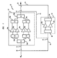
- FIG. 1 shows a typical feed-forward power amplifier architecture 10 which includes a main amplifier 12 to amplify the input signal on the main signal path 13 and a correction amplifier 14 used in reducing the distortion produced from the main amplifier 12.
- Feed-forward correction is routinely deployed in modern amplifiers to improve the linearity of the main amplifier 12 with various input patterns. The essence of the feed-forward correction is to isolate on a distortion cancellation path 16 the distortion generated by the main amplifier 12.
- a coupler 17 provides a version of the amplified input signal and distortion from the output of the main amplifier 12 onto a coupling path 18 to a coupler 19.
- a coupler 20 provides an inverse version of the input signal from the main signal path 13 to the coupler 19.
- the coupler 19 combines the amplified input signal and distortion from the coupling path with an inverse version of the input signal from the main signal path 13. As such, the input signals cancel and the distortion is left on the distortion cancellation path 16.
- the distortion is provided to the correction amplifier 14 which amplifies the distortion on the distortion cancellation path 16.
- a combiner 22 cancels the distortion on the main signal path 13 with the distortion on the distortion cancellation path 16 to reduce the distortion produced from the main amplifier 12.
- the peak power levels decrease of the signal to be amplified
- the peak power levels decrease of the distortion signal to be amplified by the correction amplifier 14.
- an amplifier can be configured as parallel amplifier stages of like amplifiers to provide the same gain as the individual amplifiers while increasing the overall power handling capability with each amplifier.
- the main amplifier 12 includes an arrangement of splitters 24a-c which split the input signal among parallel amplifiers 26a-d.
- An arrangement of combiners 28a-c combines the outputs of the parallel amplifiers 26 a-d to produce an amplified signal on the main signal path 13.
- the main amplifier 12 has the same gain as an individual amplifier 26a-n but the power handling capability of the main amplifier 12 is increased by the power handling capability of each individual amplifier 26a-d. For example, if each individual amplifier 26a-d has a 100 watts of power handling capability, the main amplifier 12 has (100 * 4) watts of power handling capability.
- the main amplifier 12 can handle peak powers of 400 watts. Peak power handling capability is important because peak power increases as the number of users increase. Because the distortion signal on the distortion cancellation path 16 is typically smaller, the correction amplifier 14 is designed in a parallel architecture to handle smaller peak powers. For example, the correction amplifier 14 includes a splitter arrangement 30 splitting the distortion signal among parallel amplifiers 32a-b, and a combiner arrangement 34 combines the amplified distortion signal. If each individual amplifier 32a-m has a power handling capability of 20 watts, the correction amplifier 14 has a power handling capability of 40 watts.
- the main amplifier 12 is the largest single contributor to the overall power consumption in CDMA, TDMA and frequency division multiple access (FDMA) base stations. Due to the potential for high peak powers, the main amplifier 12 is biased with a high current to be able to handle those peak powers when they do occur. The efficiency, however, of the main amplifiers 12 is typically less than 30%. This low efficiency leads to higher power consumption, shorter battery backup time, lower overall reliability and higher operating temperatures. Accordingly, there is a need for a more efficient power amplifier architecture.
- the present invention involves a power amplifier system using upstream signal information of a signal to be amplified by an amplifier to control the operation of the amplifier, thereby enabling the amplifier to operate more efficiently overall.
- the power amplifier system can reconfigure the amplifier based on upstream signal information, such as the measured peak power, the measured average power, the number of users, the type of carriers (CDMA, TDMA, FDMA), the number of carriers and/or the average power per carrier.
- processing circuitry can reconfigure the power amplifier architecture to adjust the peak power handling capability of the amplifier. By reducing the peak power handling capability of the amplifier, the long-term efficiency of the amplifier can be improved.
- the power amplifier system can adjust at least one operating characteristic of the amplifier while maintaining the configuration of the amplifier, for example by adjusting the bias voltage(s) to the amplifier based on upstream signal configuration information.
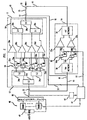
- FIG. 2 shows a general block diagram of a feed forward power amplifier architecture 40 using upstream signal information of the signal to be amplified by a main amplifier 12 to control the power handling capability of the main amplifier 12 and/or of the correction amplifier 14.
- the main amplifier 12 has parallel amplifier stages 26 a-d
- the correction amplifier 14 has parallel amplifier stages 32 a-b.
- Processing circuitry 42 receives or obtains upstream signal information on the signal to be amplified by the main amplifier 12, for example upstream signal power detection information from a power detector 44 representing the measured peak and/or average power of the signal on the main signal path 13 to be amplified by the amplifier 12.
- the processing circuitry 42 can receive upstream signal configuration information which describes the signal to be amplified without directly performing measurements on the main signal path 13, for example information on the composition, component signals and structure for the signal to be amplified, such as the number of carriers comprising the signal to be amplified, the type of carriers (for example, CDMA, TDMA or FDMA) and/or the number of users for which the signal is produced.
- the upstream signal configuration information can be provided by a base station controller (BSC) 46, the switching circuitry (MUX) and/or radio circuitry 48 to the processing circuitry 42.
- BSC base station controller
- MUX switching circuitry
- radio circuitry 48 radio circuitry
- the upstream signal information received or obtained by the processing circuitry 42 can include the upstream signal configuration information, the upstream signal power information and/or other upstream signal information.
- the processing circuitry 42 provides control signal(s) 50 to control the peak power capability of the main amplifier 12 and/or control signal(s) 52 to control the peak power capability of the correction amplifier 14.
- the processing circuitry 42 can provide control signal(s) 50 to control the peak power capability of the main amplifier 12 and/or control signal(s) 52 to control the peak power capability of the correction amplifier 14 (in this feed forward embodiment or other amplifier(s), if any, of other architectures), for example by turning “on” or “off” amplifier stages 26a-d in the main amplifier 12 and/or amplifier stages 32a-b in the correction amplifier 14.
- the processing circuitry 42 can adjust at least one operating characteristic of the main amplifier 12 and/or the correction amplifier 14 based on upstream signal configuration information or in response to the shutting down of the amplifier stage(s), for example by adjusting the bias voltage(s) and/or source voltage(s) to the amplifier 12.
- the operating characteristics of the amplifier and/or amplifier stage can include the power handling capability, including the peak power handling capability, and/or the class of operation of the amplifier.
- each individual amplifier 26a-d has a 100 watts of power handling capability
- the main amplifier 12 has 100 watts X the number of parallel power amplifier stages of power handling capability.
- the main amplifier 12 can handle peak powers of 400 watts.
- the processing circuitry 42 can provide control signal(s) to amplifier stages 26a-d to shut-off an amplifier or amplifiers, for example amplifier 26d.
- An amplifier stage 26a-d can be shut-down by cutting off the source voltage and/or the bias voltage. By shutting off an amplifier or amplifiers, the power amplifier efficiency (output power over DC power consumed) is improved because the output power effectively remains the same while the DC power consumed is reduced.
- the processing circuitry 42 can provide control signal(s) to a switching network 54 to divert the signal power for the shut-down amplifier(s) to a termination or load.
- the processing circuitry 42 can provide control signal(s) to low power radio frequency (RF) switches 55a-d which make up the switching network 54 in this embodiment.
- RF radio frequency
- the low power RF switches 55a-d route the power of the signal which would be amplified by the shut-down amplifier stage(s) to respective terminations 56a-d, and the remaining power is routed to the active amplifier stage(s) for amplification.
- the processing circuitry 42 can adjust at least one of the operating characteristics of the active amplifier stage(s), for example by adjusting the bias voltage(s) to the active amplifier stage(s), such as to increase the bias voltage(s).
- the splitting network 57 is an arrangement of 1:2 splitters 24a-c, and the splitter 24a splits the signal into two replicas of the original signal having one-half the power.
- Each splitter 24b-c receives a1/2 power replica of the original signal and splits the 1 ⁇ 2 power replica of the original signal into two 1 ⁇ 4 power replicas of the original signal, and each amplifier stage 26a-d amplifies one of the four (4) 1 ⁇ 4 power replicas of the original signal. If the amplifier stage 26d is shut-down, the processing circuitry 42 provides a control signal to the switch 55d to route the power from the switching network 57 for the amplifier stage 26d to the termination 56d, such as a 50 ohm termination.
- a combining network 58 combines the amplified copies of the signal from the active amplifier stages and combines them to provide the amplified signal at the desired level as would be understood by one of skill in the art.
- combining network 58 is an arrangement of 2:1 combiners 28a-c,
- the processing circuitry 42 can shut-off additional amplifiers, for example the amplifiers 26c-d.
- the peak power handling capability of the amplifier 12 can be adjusted by 25% increments. If the amplifier 12 has six parallel amplifier stages operating with the same operating characteristics, the peak power handling capability of the amplifier 12 could be adjusted in 16.7% increments by turning off or on amplifier stages.
- the processing circuitry 42 can provide control signal(s)to the switching network 54, for example to switches 55c-d, such that the power from the splitting network 57 for the shut-down amplifier stages 26c-d is diverted to a termination, for example respective terminations 56c-d.
- the remaining power for example from the switches 55a-b, is provided to the active amplifier stages 26a-b for amplification.
- the combining network 58 combines the amplified copies of the signal from the amplifiers 26a-b as would be unserstood by one of skil in the art.
- the power amplification architecture 40 is a feed forward arrangement where a coupler 17 provides a version of the amplified input signal and distortion from the output of the main amplifier 12 onto the coupling path 18 to the coupler 19.
- the coupler 19 combines the amplified input signal and. distortion with an inverse version of the input signal and distortion from the main signal path 13. As such, the input signals cancel, and the distortion is left on the feed forward path 16.
- the distortion is provided to the correction amplifier 14 which amplifies the distortion on the distortion cancellation path 16.
- a combiner 22 cancels the distortion on the main signal path 13 with the distortion on the feed forward path 16 to reduce the distortion produced from the main amplifier 12.
- the processing circuitry 42 can provide control signals 52 to amplifier stages 32a-b of the correction amplifier 14 to de-activate or shut-down an amplifier stage 32a-b.
- the processing circuitry 42 can provide control signal(s) 52 to switching network 62, for example of low power RF switches 64a-b, to divert the power from the splitting network 30, for example a 1:2 splitter, for the shut-down amplifier stage(s) 32a and/or b to a termination, for example to associated terminations 66a and/or b.
- the processing circuitry 42 can provide a control signal to shut-down the amplifier stage 32b, and a control signal (or the same control signal) to switch 64b to divert the power from the splitter 30 for the deactivated amplifier stage 32b to the termination 66b.
- the distortion signal can be amplified by the amplifier stage 32a and provided to the coupler 22.
- the processing circuitry 42 could shut-down both amplifier stages 32a-b and thereby the correction amplifier 14 depending on the upstream signal information.
- the power amplification system according to principles of the present invention can operate with other power amplifier architectures which use different structures and do not use a correction amplifier 14 as described above to reduce the nonlinear distortion of the signal.
- the correction amplifier 14 can be replaced with a second amplifier or amplifiers in an arrangement where the amplifiers amplify versions of the original signal, and the amplified versions of the original signal are combined to produce the amplified signal while producing reduced distortion.
- Other power amplification architectures are possible.
- the processing circuitry 42 receives upstream signal power detection information comprising peak power information of a signal, such as a multicarrier signal, on the path 13 after the signal multiplexer/combiner 60 and before the amplifier 12.
- the processing circuitry 42 can determine the peak power demand of the signal to be amplified and/or can provide control signal(s) 50 to control the peak power capability of the main amplifier 12 and/or control signal(s) 52 to control the peak power capability of the correction amplifier 14 (in this feed forward embodiment or other amplifier(s), if any, of other architectures).
- the processing circuitry can reconfigure the amplifier 12 and/or the correction amplifier 14, for example by turning “on” or “off” amplifier stages 26a-d in the main amplifier 12 and/or amplifier stages 32a-b in the correction amplifier 14 as well as providing control signals to switching and/or combining networks 54, 58, 62 and/or 32. Additionally, based on the upstream signal power detection information or the reconfiguration of the amplifier(s), the processing circuitry 42 can further change the power handling capability and/or the operating characteristics of the active amplifier stage(s), for example by changing the bias voltage(s) to the active amplifier stage(s).
- the processing circuitry 42 receives upstream signal configuration information, for example the number of carriers comprising the signal to be amplified and the type of carriers (for example, CDMA, TDMA or FDMA).
- upstream signal configuration information for example the number of carriers comprising the signal to be amplified and the type of carriers (for example, CDMA, TDMA or FDMA).
- the processing circuitry 42 can reconfigure the amplifier 12 and/or the correction amplifier 14 (in this feed forward embodiment or other amplifier(s), if any, of other architectures). For example, using the upstream signal configuration information, processing circuitry 42 can determine a peak power demand of the signal to be amplified.
- the Gain is the gain of the amplifer 12
- the peak to average power ratio factor P factor can be determined using upstream signal configuration information, for example the type of carriers and/or the number of carriers.
- P factor can be 8dB for an FDMA carrier, 9dB for a TDMA carrier and 11.3 dB for a CDMA carrier type. These values may be determined based on the number of carriers or further changed for known type of carriers based on the number of carriers.
- the P demand ,P avg ,Gain and/or P factor can be provided as upstream signal configuration information or used to determine or provide upstream signal configuration information by determining peak power demand given upstream signal configuration information or providing the peak power demand by providing the upstream signal configuration information to a look-up table.
- the processing circuitry can provide control signal(s) 50 to control the peak power capability of the main amplifier 12 and/or control signal(s) 52 to control the peak power capability of the correction amplifier 14 (in this feed forward embodiment).
- the processing circuitry 42 can reconfigure the amplifer 12 and/or the correction amplifier 14 by turning “on” or “off' amplifier stages 26a-d in the main amplifier 12 and/or amplifier stages 32a-b in the correction amplifier 14 as well as providing control signal(s) to switching and/or combining networks 54, 58 62 and/or 34.
- the processing circuitry 42 can change the power handling capability and/or the operating characteristics, such as operating class of the main amplifier 12, the correction amplifier 14 (in this feed forward embodiment or other amplifier(s), if any, of other architectures) and/or of the amplifier stage(s) 26a-d or 32a-b, for example by changing the bias voltage(s) to the amplifier stage(s).
- the processing circuitry 42 can receive upstream signal information which includes both upstream signal configuration information and upstream signal power detection information, for example the average power and/or the peak power of the signal on the path 13 after the multiplexer or combiner 60 and before the main amplifier 12 and the type of carriers and/or number of carriers comprising the signal to be amplified.
- upstream signal configuration information and the upstream signal power detection information the processing circuitry 42 can reconfigure the amplifier 12 and/or the correction amplifier 14 (in this feed forward embodiment or other amplifier(s), if any, of other architectures). For example, using the upstream signal configuration information and the upstream signal power detection information, the processing circuitry 42 can determine a peak power demand for the signal to be amplified.
- P avg can be measured as upstream signal power detection information by power detector 44 at the input to the amplifier 12 and P factor can be determined by the type of carriers and/or the number of carriers as upstream signal configuration information.
- the processing circuitry can provide control signal(s) 50 to control the peak power capability of the main amplifier 12 and/or control signal(s) 52 to control the peak power capability of the correction amplifier 14 (in this feed forward embodiment).
- the processing circuitry 42 can reconfigure the amplifier 12 and/or the correction amplifier 14 by turning “on” or “off” amplifier stages 26a-d in the main amplifier 12 and/or amplifier stages 32a-b in the correction amplifier 14 as well as providing control signal(s) to switching and/or combining networks 54, 58, 30 and/or 34 as described above.
- the processing circuitry 42 can change the power handling capability and/or the operating characteristics, such as the operating class of the main amplifier 12, the correction amplifier 14 (in this feed forward embodiment or other amplifier(s), if any, of other architectures) and/or of the amplifier stage(s) 26a-d or 32a-b, for example by changing the bias voltage(s) to the amplifier stage(s).
- the processing circuitry 42 can use the upstream signal configuration information to determine a peak power demand, and reconfigure and/or change the operating characteristics or peak power handling capability of the main amplifier 12 and/or the correction amplifier 14 to efficiently handle such peak powers determined for the signals characterized by the upstream signal configuration information. Furthermore, the processing circuitry can further receive upstream signal power detection information, such as the actual peak power of the signal to be amplified, to further reconfigure the main amplifier 12 and/or the correction amplifier 14 (in this feed forward embodiment or other amplifier(s), if any, of other architectures) and/or control the operating characteristics of the amplifier stage(s).
- upstream signal power detection information such as the actual peak power of the signal to be amplified
- the processing circuitry 42 can provide control signal(s) to reconfigure the amplifier (s) by shutting-down amplifier stage(s) based on the upstream signal information and changing the operating characteristics of the active amplifier stage(s) based on the upstream signal information or in response to the reconfiguration, for example by adjusting the bias voltage(s) of the operating amplifier stage(s).
- the power amplification system has been described as determining a peak power demand from the upstream signal information to control the amplifier(s), but embodiments of the amplification system can control the reconfiguration and/or operation of the amplifier(s) and/or the amplifier stages(s) based on upstream signal information without affirmatively calculating peak power demand from the upstream signal information, for example if the upstream signal information is input to a look-up table which produces particular control signal(s) to control the reconfiguration and/or operating characteristics of the amplifier(s) and/or amplifier stage(s).
- the upstream signal information can include or be the peak power demand.
- the embodiments of the power amplification system have been described as being used with a particular feed-forward RF amplifier arrangement, but the architecture can be used to improve signal amplification in other amplifier or electrical circuit arrangements.
- the main amplifier 12 can be the only amplifier, and there is no correction amplifier. Additional amplifier(s) can be used to amplify replicas of the original signal which are recombined to produce the amplified signal.
- Other architectures are possible which use combinations of the above described architectures and/or techniques for amplifying a signal in a more efficient and/or linear fashion.
- the power architecture system has been described as detecting certain upstream signal information, but other parameters or characteristics of the signal to be amplified can be detected along with the upstream signal information or as the upstream signal information.
- the system has also been described as shutting off or on particular amplifier stage(s), but the amplifier stage(s) which shut off or on can be rotated or changed in any desired manner.
- the system has been described as using couplers, splitters and combiners, but other devices, such as 3dB splitters and other coupling, signal splitting, or sampling devices, can be used as well as other combining arrangements or devices, such as summers.
- the power amplifier architecture has been further described as using different configurations using discrete components, but it should be understood that the architecture and portions thereof can be implemented in application specific integrated circuits, software-driven processing circuitry, firmware or other arrangements of discrete components as would be understood by one of ordinary skill in the art with the benefit of this disclosure. What has been described is merely illustrative of the application of the principles of the present invention. Those skilled in the art will readily recognize that these and various other modifications, arrangements and methods can be made to the present invention without strictly following the exemplary applications illustrated and described herein and without departing from the spirit and scope of the present invention.
Abstract
Description
- This invention relates to amplifiers and, more particularly, to a power amplifier which uses upstream signal information.
- An ideal power amplifier amplifies an input signal with no waveshape alteration. The ideal power amplifier is therefore characterized as having a transfer function (input signal vs. output signal) which is linear with no transfer function discontinuities. In practice, a power amplifier, however, has a transfer function with nonlinear and "linear" regions. Whether the power amplifier is operating in a linear or nonlinear region depends on the amplitude of the input signal. For the power amplifier to achieve as near to linear operation as possible, the power amplifier is designed to operate within its linear region given the range of possible input signal amplitudes. If the input signal has an amplitude which causes the power amplifier to operate outside the linear region, the power amplifier introduces nonlinear components or distortion to the signal. When the input signal possesses peak amplitudes which cause the amplifier to compress, to saturate (no appreciable increase in output amplitude with an increase in input amplitude) or to shut-off (no appreciable decrease in output amplitude with a decrease in input amplitude), the amplifer is being overdriven, and the output signal is clipped or distorted in a nonlinear fashion. In addition to distorting the signal, the clipping or nonlinear distortion of the input signal, generates spectral regrowth or adjacent channel power (ACP) that can interfere with an adjacent frequency.
- In wireless communications systems, high power amplification of signals for transmission are commonly encountered with very large peak to average power ratios (PAR). For example, in a time division multiple access (TDMA) system, when multiple carriers signals are combined for amplification with a power amplifier, the resulting PAR is about 9 dB for a large number of carriers. In a code division multiple access (CDMA) system, a single loaded 1.25 Mhz wide carrier can have a PAR of 11.3 dB. These signals have to be amplified fairly linearly to avoid generating ACP. To satisfy the linearity requirement, power amplifiers are usually operated in Class A and Class AB configurations. To be able to handle large peaks, the amplifiers are biased at high bias currents. The efficiency of the amplifiers is low because of the high bias and the high peak to average power ratios.
- Accordingly, efficiency of the amplifier is inversely related to the ability to handle high peaks in a linear fashion. To achieve a high degree of linearity, the amplifiers are biased to operate in class A or "slight" class AB (meaning class AB operation that is closer to class A than to class B). Maximum AC to DC efficiency achievable for class A operation is 50%, whereas that of a class AB amplifier is between 50 and 78.5% (the latter representing the maximum efficiency of a class B amplifier). The closer the particular class AB operation is to class A, the lower the maximum efficiency. For amplifiers employing field effect transistors, the class of operation is set in accordance with the gate voltage applied, which controls the quiescent (idle) drain current. For class A operation, the gate voltage is set so that the idle drain current is approximately in the middle of the range between pinch-off and saturation. Class B amplifiers are biased near pinch-off, resulting in a rectified drain current waveform. Class AB amplifiers are biased in between the bias points of classes A and B.
- Typically, strict linearity requirements in modern wireless communication systems dictate the use of the relatively inefficient class A or slight class AB modes. As a result, significant DC power is dissipated by the amplifiers, thereby generating heat which must be controlled to avoid degrading amplifier performance and reliability. Hence, the use of elaborate heat sinks and fans become a necessary by-product of the high linearity system. Naturally, these measures add to the cost, size and weight of the base station equipment. As the number of wireless communications users continues to grow, so do the number of base stations and the need to keep them small, light and inexpensive. Thus, a great deal of research has focused on the quest to improve amplifier efficiency in these and other systems.
- Various methods are used to enable the use of more cost-effective and more power efficient amplifiers while maintaining an acceptable level of linearity. Feed-forward correction is routinely deployed in modern amplifiers to improve the linearity of the main amplifier with various input patterns. The essence of the feed-forward correction is to isolate the distortion generated by the main amplifier on a feed forward path. The distortion is provided to a correction amplifier on the feed forward path which amplifies the distortion. The distortion on the feed forward path is combined with the distortion on the main signal path to cancel the distortion on the main signal path. Pre-distortion techniques distort the input signal prior to amplification by taking into account the transfer function characteristics for the amplifier. As such, the desired amplified signal is achieved from the pre-distorted input signal. These techniques help to improve the efficiency of the amplifier while maintaining linearity, but to be able to handle the large peaks of a signal, the amplifiers still operate inefficiently. A technique described by Adel A.M. Saleh and Donald C. Cox, "Improving the Power-Added Efficiency of FET Amplifiers Operating with Varying Envelope Signals," IEEE Transactions On Microwave Theory and Techniques, Vol. 31, No. 1, January 1983 uses the input signal envelope to dynamically adjust the amplifier bias such that a high bias is only applied when a large peak is encountered.
- Wireless base stations use a variety of radio frequency (RF) amplifers in both single carrier and multicarrier configurations operating in Class A and Class AB modes. FIG. 1 shows a typical feed-forward
power amplifier architecture 10 which includes amain amplifier 12 to amplify the input signal on themain signal path 13 and acorrection amplifier 14 used in reducing the distortion produced from themain amplifier 12. Feed-forward correction is routinely deployed in modern amplifiers to improve the linearity of themain amplifier 12 with various input patterns. The essence of the feed-forward correction is to isolate on adistortion cancellation path 16 the distortion generated by themain amplifier 12. To isolate the distortion on the distortion cancellation or feedforward path 16, acoupler 17 provides a version of the amplified input signal and distortion from the output of themain amplifier 12 onto acoupling path 18 to acoupler 19. Acoupler 20 provides an inverse version of the input signal from themain signal path 13 to thecoupler 19. Thecoupler 19 combines the amplified input signal and distortion from the coupling path with an inverse version of the input signal from themain signal path 13. As such, the input signals cancel and the distortion is left on thedistortion cancellation path 16. The distortion is provided to thecorrection amplifier 14 which amplifies the distortion on thedistortion cancellation path 16. Acombiner 22 cancels the distortion on themain signal path 13 with the distortion on thedistortion cancellation path 16 to reduce the distortion produced from themain amplifier 12. In general, as the peak power levels decrease of the signal to be amplified, the peak power levels decrease of the distortion signal to be amplified by thecorrection amplifier 14. - Other power amplifier architectures are possible which use different structures and do not use a
correction amplifier 14 as described above to reduce the nonlinear distortion of the signal. For example, thecorrection amplifier 14 can be replaced with a second amplifier or amplifiers in an arrangement where the amplifiers amplify versions of the original signal, and the amplified versions of the original signal are combined to produce the amplified signal while producing reduced distortion. For example, U.S. Patent No. 5,917,375 issued on June 29, 1999 entitled "Low Distortion Amplifier Circuit with Improved Output Power" describes a power amplification architecture using multiple amplifiers. Other power amplification architectures use pre-distortion techniques and baseband processing techniques to improve the efficiency and/or linearity of the power amplification architecture. - To achieve higher output powers, an amplifier can be configured as parallel amplifier stages of like amplifiers to provide the same gain as the individual amplifiers while increasing the overall power handling capability with each amplifier. The
main amplifier 12 includes an arrangement of splitters 24a-c which split the input signal amongparallel amplifiers 26a-d. An arrangement ofcombiners 28a-c combines the outputs of the parallel amplifiers 26 a-d to produce an amplified signal on themain signal path 13. Themain amplifier 12 has the same gain as anindividual amplifier 26a-n but the power handling capability of themain amplifier 12 is increased by the power handling capability of eachindividual amplifier 26a-d. For example, if eachindividual amplifier 26a-d has a 100 watts of power handling capability, themain amplifier 12 has (100 * 4) watts of power handling capability. Thus, themain amplifier 12 can handle peak powers of 400 watts. Peak power handling capability is important because peak power increases as the number of users increase. Because the distortion signal on thedistortion cancellation path 16 is typically smaller, thecorrection amplifier 14 is designed in a parallel architecture to handle smaller peak powers. For example, thecorrection amplifier 14 includes asplitter arrangement 30 splitting the distortion signal amongparallel amplifiers 32a-b, and acombiner arrangement 34 combines the amplified distortion signal. If eachindividual amplifier 32a-m has a power handling capability of 20 watts, thecorrection amplifier 14 has a power handling capability of 40 watts. - As such, in the described feed forward architecture, the
main amplifier 12 is the largest single contributor to the overall power consumption in CDMA, TDMA and frequency division multiple access (FDMA) base stations. Due to the potential for high peak powers, themain amplifier 12 is biased with a high current to be able to handle those peak powers when they do occur. The efficiency, however, of themain amplifiers 12 is typically less than 30%. This low efficiency leads to higher power consumption, shorter battery backup time, lower overall reliability and higher operating temperatures. Accordingly, there is a need for a more efficient power amplifier architecture. - The present invention involves a power amplifier system using upstream signal information of a signal to be amplified by an amplifier to control the operation of the amplifier, thereby enabling the amplifier to operate more efficiently overall. The power amplifier system can reconfigure the amplifier based on upstream signal information, such as the measured peak power, the measured average power, the number of users, the type of carriers (CDMA, TDMA, FDMA), the number of carriers and/or the average power per carrier. For example, based on upstream signal information for the signal to be amplified, processing circuitry can reconfigure the power amplifier architecture to adjust the peak power handling capability of the amplifier. By reducing the peak power handling capability of the amplifier, the long-term efficiency of the amplifier can be improved. The power amplifier system can adjust at least one operating characteristic of the amplifier while maintaining the configuration of the amplifier, for example by adjusting the bias voltage(s) to the amplifier based on upstream signal configuration information.
- Other aspects and advantages of the present invention may become apparent upon reading the following detailed description and upon reference to the drawings in which:
- FIG. 1 shows a power amplifier architecture which can use upstream signal information according to the principles of the present invention; and
- FIG. 2 shows the power amplifier architecture using upstream information according to the principles of the present invention.
-
- An illustrative embodiment of a power amplifier system using upstream information according to the principles of the present invention is described. FIG. 2 shows a general block diagram of a feed forward
power amplifier architecture 40 using upstream signal information of the signal to be amplified by amain amplifier 12 to control the power handling capability of themain amplifier 12 and/or of thecorrection amplifier 14. In this embodiment, themain amplifier 12 has parallel amplifier stages 26 a-d, and thecorrection amplifier 14 has parallel amplifier stages 32 a-b.Processing circuitry 42 receives or obtains upstream signal information on the signal to be amplified by themain amplifier 12, for example upstream signal power detection information from a power detector 44 representing the measured peak and/or average power of the signal on themain signal path 13 to be amplified by theamplifier 12. Additionally or alternatively, theprocessing circuitry 42 can receive upstream signal configuration information which describes the signal to be amplified without directly performing measurements on themain signal path 13, for example information on the composition, component signals and structure for the signal to be amplified, such as the number of carriers comprising the signal to be amplified, the type of carriers (for example, CDMA, TDMA or FDMA) and/or the number of users for which the signal is produced. The upstream signal configuration information can be provided by a base station controller (BSC) 46, the switching circuitry (MUX) and/orradio circuitry 48 to theprocessing circuitry 42. Theprocessing circuitry 42 or portions thereof can be located in theBSC 46, the switching circuitry (MUX) and/or theradio circuitry 48. - Depending on the embodiment, the upstream signal information received or obtained by the
processing circuitry 42 can include the upstream signal configuration information, the upstream signal power information and/or other upstream signal information. In response to the upstream signal information, theprocessing circuitry 42 provides control signal(s) 50 to control the peak power capability of themain amplifier 12 and/or control signal(s) 52 to control the peak power capability of thecorrection amplifier 14. Based on the upstream signal information, theprocessing circuitry 42 can provide control signal(s) 50 to control the peak power capability of themain amplifier 12 and/or control signal(s) 52 to control the peak power capability of the correction amplifier 14 (in this feed forward embodiment or other amplifier(s), if any, of other architectures), for example by turning "on" or "off" amplifier stages 26a-d in themain amplifier 12 and/oramplifier stages 32a-b in thecorrection amplifier 14. Depending on the embodiment, theprocessing circuitry 42 can adjust at least one operating characteristic of themain amplifier 12 and/or thecorrection amplifier 14 based on upstream signal configuration information or in response to the shutting down of the amplifier stage(s), for example by adjusting the bias voltage(s) and/or source voltage(s) to theamplifier 12. The operating characteristics of the amplifier and/or amplifier stage can include the power handling capability, including the peak power handling capability, and/or the class of operation of the amplifier. - In this embodiment, if each
individual amplifier 26a-d has a 100 watts of power handling capability, themain amplifier 12 has 100 watts X the number of parallel power amplifier stages of power handling capability. As such, themain amplifier 12 can handle peak powers of 400 watts. If the detected power level of the signal to be amplified is below a particular level, for example 300 watts, theprocessing circuitry 42 can provide control signal(s) toamplifier stages 26a-d to shut-off an amplifier or amplifiers, forexample amplifier 26d. Anamplifier stage 26a-d can be shut-down by cutting off the source voltage and/or the bias voltage. By shutting off an amplifier or amplifiers, the power amplifier efficiency (output power over DC power consumed) is improved because the output power effectively remains the same while the DC power consumed is reduced. - In response to or based on the upstream signal information or in response to the turning off of an amplifier(s) or amplifier stage(s), the
processing circuitry 42 can provide control signal(s) to aswitching network 54 to divert the signal power for the shut-down amplifier(s) to a termination or load. For example, theprocessing circuitry 42 can provide control signal(s) to low power radio frequency (RF) switches 55a-d which make up theswitching network 54 in this embodiment. In response to the control signal(s), the low power RF switches 55a-d route the power of the signal which would be amplified by the shut-down amplifier stage(s) torespective terminations 56a-d, and the remaining power is routed to the active amplifier stage(s) for amplification. Based on the upstream signal information or in response to the amplifier stage(s) which are shut-down, theprocessing circuitry 42 can adjust at least one of the operating characteristics of the active amplifier stage(s), for example by adjusting the bias voltage(s) to the active amplifier stage(s), such as to increase the bias voltage(s). - In this embodiment, the
splitting network 57 is an arrangement of 1:2 splitters 24a-c, and the splitter 24a splits the signal into two replicas of the original signal having one-half the power. Eachsplitter 24b-c receives a1/2 power replica of the original signal and splits the ½ power replica of the original signal into two ¼ power replicas of the original signal, and eachamplifier stage 26a-d amplifies one of the four (4) ¼ power replicas of the original signal. If theamplifier stage 26d is shut-down, theprocessing circuitry 42 provides a control signal to theswitch 55d to route the power from the switchingnetwork 57 for theamplifier stage 26d to thetermination 56d, such as a 50 ohm termination. The remaining power, for example from theswitches 55a-c, is provided to theactive amplifier stages 26a-c for amplification. After amplification, a combiningnetwork 58 combines the amplified copies of the signal from the active amplifier stages and combines them to provide the amplified signal at the desired level as would be understood by one of skill in the art. In this embodiment, combiningnetwork 58 is an arrangement of 2:1combiners 28a-c, - If the power level of the signal to be amplified is even lower, for example below a second threshold level (such as 200 watts or 50% of the total peak power handling capability of the amplifier 12), the
processing circuitry 42 can shut-off additional amplifiers, for example theamplifiers 26c-d. In this embodiment with four similar or the sameparallel amplifier stages 26a-d with the same operating characteristics, the peak power handling capability of theamplifier 12 can be adjusted by 25% increments. If theamplifier 12 has six parallel amplifier stages operating with the same operating characteristics, the peak power handling capability of theamplifier 12 could be adjusted in 16.7% increments by turning off or on amplifier stages. As such, theprocessing circuitry 42 can provide control signal(s)to theswitching network 54, for example to switches 55c-d, such that the power from thesplitting network 57 for the shut-down amplifier stages 26c-d is diverted to a termination, for examplerespective terminations 56c-d. The remaining power, for example from theswitches 55a-b, is provided to theactive amplifier stages 26a-b for amplification. After amplification, the combiningnetwork 58 combines the amplified copies of the signal from theamplifiers 26a-b as would be unserstood by one of skil in the art. - In the embodiment of FIG. 2, the
power amplification architecture 40 is a feed forward arrangement where acoupler 17 provides a version of the amplified input signal and distortion from the output of themain amplifier 12 onto thecoupling path 18 to thecoupler 19. Thecoupler 19 combines the amplified input signal and. distortion with an inverse version of the input signal and distortion from themain signal path 13. As such, the input signals cancel, and the distortion is left on the feedforward path 16. The distortion is provided to thecorrection amplifier 14 which amplifies the distortion on thedistortion cancellation path 16. Acombiner 22 cancels the distortion on themain signal path 13 with the distortion on the feedforward path 16 to reduce the distortion produced from themain amplifier 12. As the peak power levels decrease of the signal to be amplified, the peak power levels decrease of the distortion signal to be amplified by thecorrection amplifier 14. Accordingly, theprocessing circuitry 42 can providecontrol signals 52 toamplifier stages 32a-b of thecorrection amplifier 14 to de-activate or shut-down anamplifier stage 32a-b. - The
processing circuitry 42 can provide control signal(s) 52 to switchingnetwork 62, for example of low power RF switches 64a-b, to divert the power from thesplitting network 30, for example a 1:2 splitter, for the shut-down amplifier stage(s) 32a and/or b to a termination, for example to associated terminations 66a and/or b. For example, theprocessing circuitry 42 can provide a control signal to shut-down theamplifier stage 32b, and a control signal (or the same control signal) to switch 64b to divert the power from thesplitter 30 for the deactivatedamplifier stage 32b to thetermination 66b. As such, the distortion signal can be amplified by theamplifier stage 32a and provided to thecoupler 22. Depending on the embodiment, theprocessing circuitry 42 could shut-down bothamplifier stages 32a-b and thereby thecorrection amplifier 14 depending on the upstream signal information. - The power amplification system according to principles of the present invention can operate with other power amplifier architectures which use different structures and do not use a
correction amplifier 14 as described above to reduce the nonlinear distortion of the signal. For example, thecorrection amplifier 14 can be replaced with a second amplifier or amplifiers in an arrangement where the amplifiers amplify versions of the original signal, and the amplified versions of the original signal are combined to produce the amplified signal while producing reduced distortion. Other power amplification architectures are possible. - In one embodiment, the
processing circuitry 42 receives upstream signal power detection information comprising peak power information of a signal, such as a multicarrier signal, on thepath 13 after the signal multiplexer/combiner 60 and before theamplifier 12. In response to the peak power information, theprocessing circuitry 42 can determine the peak power demand of the signal to be amplified and/or can provide control signal(s) 50 to control the peak power capability of themain amplifier 12 and/or control signal(s) 52 to control the peak power capability of the correction amplifier 14 (in this feed forward embodiment or other amplifier(s), if any, of other architectures). In response to peak power demand and/or the upstream signal power detection information, the processing circuitry can reconfigure theamplifier 12 and/or thecorrection amplifier 14, for example by turning "on" or "off" amplifier stages 26a-d in themain amplifier 12 and/oramplifier stages 32a-b in thecorrection amplifier 14 as well as providing control signals to switching and/or combiningnetworks processing circuitry 42 can further change the power handling capability and/or the operating characteristics of the active amplifier stage(s), for example by changing the bias voltage(s) to the active amplifier stage(s). - In an alternative embodiment, the
processing circuitry 42 receives upstream signal configuration information, for example the number of carriers comprising the signal to be amplified and the type of carriers (for example, CDMA, TDMA or FDMA). In response to the upstream signal configuration information, theprocessing circuitry 42 can reconfigure theamplifier 12 and/or the correction amplifier 14 (in this feed forward embodiment or other amplifier(s), if any, of other architectures).
For example, using the upstream signal configuration information,processing circuitry 42 can determine a peak power demand of the signal to be amplified. For example, peak power demand can be determined as Pdemand = Pavg + Gain + Pfactor, where Pavg is the average power of the signal at the input to theamplifier 12 which can be provided or determined by knowing the number of carriers or users in the signal and the average power per carrier as upstream signal configuration information. The Gain is the gain of theamplifer 12, and the peak to average power ratio factor Pfactor can be determined using upstream signal configuration information, for example the type of carriers and/or the number of carriers. For example, Pfactor can be 8dB for an FDMA carrier, 9dB for a TDMA carrier and 11.3 dB for a CDMA carrier type. These values may be determined based on the number of carriers or further changed for known type of carriers based on the number of carriers. Depending on the embodiment, the Pdemand ,Pavg ,Gain and/or Pfactor can be provided as upstream signal configuration information or used to determine or provide upstream signal configuration information by determining peak power demand given upstream signal configuration information or providing the peak power demand by providing the upstream signal configuration information to a look-up table. - In response to the peak power demand and/or the upstream signal configuration information, the processing circuitry can provide control signal(s) 50 to control the peak power capability of the
main amplifier 12 and/or control signal(s) 52 to control the peak power capability of the correction amplifier 14 (in this feed forward embodiment). Theprocessing circuitry 42 can reconfigure theamplifer 12 and/or thecorrection amplifier 14 by turning "on" or "off'amplifier stages 26a-d in themain amplifier 12 and/oramplifier stages 32a-b in thecorrection amplifier 14 as well as providing control signal(s) to switching and/or combiningnetworks processing circuitry 42 can change the power handling capability and/or the operating characteristics, such as operating class of themain amplifier 12, the correction amplifier 14 (in this feed forward embodiment or other amplifier(s), if any, of other architectures) and/or of the amplifier stage(s) 26a-d or 32a-b, for example by changing the bias voltage(s) to the amplifier stage(s). - Furthermore, the
processing circuitry 42 can receive upstream signal information which includes both upstream signal configuration information and upstream signal power detection information, for example the average power and/or the peak power of the signal on thepath 13 after the multiplexer orcombiner 60 and before themain amplifier 12 and the type of carriers and/or number of carriers comprising the signal to be amplified. In response to the upstream signal configuration information and the upstream signal power detection information, theprocessing circuitry 42 can reconfigure theamplifier 12 and/or the correction amplifier 14 (in this feed forward embodiment or other amplifier(s), if any, of other architectures). For example, using the upstream signal configuration information and the upstream signal power detection information, theprocessing circuitry 42 can determine a peak power demand for the signal to be amplified. For example, as mentioned above, if Pdemand = Pavg + Gain + Pfactor, Pavg can be measured as upstream signal power detection information by power detector 44 at the input to theamplifier 12 and Pfactor can be determined by the type of carriers and/or the number of carriers as upstream signal configuration information. - In response to the peak power demand and/or the upstream signal information, the processing circuitry can provide control signal(s) 50 to control the peak power capability of the
main amplifier 12 and/or control signal(s) 52 to control the peak power capability of the correction amplifier 14 (in this feed forward embodiment). Theprocessing circuitry 42 can reconfigure theamplifier 12 and/or thecorrection amplifier 14 by turning "on" or "off" amplifier stages 26a-d in themain amplifier 12 and/oramplifier stages 32a-b in thecorrection amplifier 14 as well as providing control signal(s) to switching and/or combiningnetworks processing circuitry 42 can change the power handling capability and/or the operating characteristics, such as the operating class of themain amplifier 12, the correction amplifier 14 (in this feed forward embodiment or other amplifier(s), if any, of other architectures) and/or of the amplifier stage(s) 26a-d or 32a-b, for example by changing the bias voltage(s) to the amplifier stage(s). - Depending on the embodiment, the
processing circuitry 42 can use the upstream signal configuration information to determine a peak power demand, and reconfigure and/or change the operating characteristics or peak power handling capability of themain amplifier 12 and/or thecorrection amplifier 14 to efficiently handle such peak powers determined for the signals characterized by the upstream signal configuration information. Furthermore, the processing circuitry can further receive upstream signal power detection information, such as the actual peak power of the signal to be amplified, to further reconfigure themain amplifier 12 and/or the correction amplifier 14 (in this feed forward embodiment or other amplifier(s), if any, of other architectures) and/or control the operating characteristics of the amplifier stage(s). Additionally, theprocessing circuitry 42 can provide control signal(s) to reconfigure the amplifier (s) by shutting-down amplifier stage(s) based on the upstream signal information and changing the operating characteristics of the active amplifier stage(s) based on the upstream signal information or in response to the reconfiguration, for example by adjusting the bias voltage(s) of the operating amplifier stage(s). - In addition to the embodiment described above, alternative configurations of the power amplification architecture according to the principles of the present invention are possible which omit and/or add components and/or use variations or portions of the described system. For example, the power amplification system has been described as determining a peak power demand from the upstream signal information to control the amplifier(s), but embodiments of the amplification system can control the reconfiguration and/or operation of the amplifier(s) and/or the amplifier stages(s) based on upstream signal information without affirmatively calculating peak power demand from the upstream signal information, for example if the upstream signal information is input to a look-up table which produces particular control signal(s) to control the reconfiguration and/or operating characteristics of the amplifier(s) and/or amplifier stage(s). Moreover, the upstream signal information can include or be the peak power demand. Additionally, the embodiments of the power amplification system have been described as being used with a particular feed-forward RF amplifier arrangement, but the architecture can be used to improve signal amplification in other amplifier or electrical circuit arrangements. Depending on the embodiment, the
main amplifier 12 can be the only amplifier, and there is no correction amplifier. Additional amplifier(s) can be used to amplify replicas of the original signal which are recombined to produce the amplified signal. Other architectures are possible which use combinations of the above described architectures and/or techniques for amplifying a signal in a more efficient and/or linear fashion. - Furthermore, the power architecture system has been described as detecting certain upstream signal information, but other parameters or characteristics of the signal to be amplified can be detected along with the upstream signal information or as the upstream signal information. The system has also been described as shutting off or on particular amplifier stage(s), but the amplifier stage(s) which shut off or on can be rotated or changed in any desired manner. The system has been described as using couplers, splitters and combiners, but other devices, such as 3dB splitters and other coupling, signal splitting, or sampling devices, can be used as well as other combining arrangements or devices, such as summers. The power amplifier architecture has been further described as using different configurations using discrete components, but it should be understood that the architecture and portions thereof can be implemented in application specific integrated circuits, software-driven processing circuitry, firmware or other arrangements of discrete components as would be understood by one of ordinary skill in the art with the benefit of this disclosure. What has been described is merely illustrative of the application of the principles of the present invention. Those skilled in the art will readily recognize that these and various other modifications, arrangements and methods can be made to the present invention without strictly following the exemplary applications illustrated and described herein and without departing from the spirit and scope of the present invention.
Claims (15)
- A method of amplifying a signal with an amplifier (12) having a first configuration, said method CHARACTERIZED BY:obtaining upstream signal information of said signal to be amplified by said amplifier; andreconfiguring said amplifier (12) to a second configuration based on said upstream signal information.
- The method of claim 1 CHARACTERIZED IN THAT said obtaining including:
measuring at least one of the average power and peak power of the signal to be amplified as said upstream signal information. - The method of claim 1 CHARACTERIZED IN THAT said obtaining including:
obtaining as said upstream signal information upstream signal configuration information comprising at least one of the number of carriers comprising the signal to be amplified, the type of carriers, the number of users, and the average power per carrier. - The method of claim 1 CHARACTERIZED IN THAT said reconfiguring including:
turning off at least one amplifier stage (26a, 26b, 26c, 26d) of said amplifier (12) based on said upstream signal information. - The method of claim 4 CHARACTERIZED IN THAT said reconfiguring including:determining peak power demand of said signal to be amplified using the upstream signal information; andturning off at least one amplifier stage (26a, 26b, 26c, 26d) of said amplifier based on said peak power demand.
- The method of claim 1 CHARACTERIZED IN THAT said reconfiguring including:
switching power for an amplifier stage (26a, 26b, 26c, 26d) which is shut-down to a termination (56a, 56b, 56c, 56d). - The method of claim 1 CHARACTERIZED BY:
adjusting at least one operating characteristic of said amplifier based (12) on said upstream signal information. - A power amplification system, said system CHARACTERIZED BY:an amplifier (12) having a first configuration which receives a signal to be amplified; andprocessing circuitry (42) responsive to upstream signal information to provide at least one control signal to said amplifier (12) to reconfigure said amplifier (12) to a second configuration.
- The system of claim 8 wherein said processing circuitry (42) configured to measure at least one of the average power and peak power of the signal to be amplified as said upstream signal information.
- The system of claim 9 CHARACTERIZED IN THAT said processing circuitry (42) further configured to use, as said upstream signal information, upstream signal configuration information comprising at least one of the number of carriers comprising the signal to be amplified, the type of carriers and the number of users.
- A method of amplifying a signal with an amplifier (12), said method
CHARACTERIZED BY:obtaining upstream signal configuration information of said signal to be amplified by said amplifier (12); andadjusting at least one operating characteristic of said amplifier (12) based on said upstream signal configuration information. - The method of claim 11 CHARACTERIZED IN THAT said obtaining including:
obtaining said upstream signal configuration information comprising at least one of the number of carriers comprising the signal to be amplified, the type of carriers and the number of user. - The method of claim 11 CHARACTERIZED IN THAT said adjusting including:
turning "on" or "off" amplifier stages (26a, 26b, 26c, 26d) comprising said amplifier (12) based on said upstream signal configuration information. - A power amplification system, said system CHARACTERIZED BY:an amplifier (12) which receives a signal to be amplified; andprocessing circuitry (42) responsive to upstream signal configuration information to provide at least one control signal to said amplifier (12) to adjust at least one operating characteristic of said amplifier (12) based on said upstream signal configuration information.
- The system of claim 141 CHARACTERIZED IN THAT said processing circuitry (42) configured to receive said upstream signal configuration information comprising at least one of the number of carriers comprising the signal to be amplified, the type of carriers and the number of users.
Applications Claiming Priority (2)
| Application Number | Priority Date | Filing Date | Title |
|---|---|---|---|
| US09/494,082 US6359504B1 (en) | 2000-01-28 | 2000-01-28 | Power amplifier using upstream signal information |
| US494082 | 2000-01-28 |
Publications (3)
| Publication Number | Publication Date |
|---|---|
| EP1120904A2 true EP1120904A2 (en) | 2001-08-01 |
| EP1120904A3 EP1120904A3 (en) | 2004-06-30 |
| EP1120904B1 EP1120904B1 (en) | 2012-03-21 |
Family
ID=23962955
Family Applications (1)
| Application Number | Title | Priority Date | Filing Date |
|---|---|---|---|
| EP01300308A Expired - Lifetime EP1120904B1 (en) | 2000-01-28 | 2001-01-15 | Power amplifier using upstream signal information |
Country Status (7)
| Country | Link |
|---|---|
| US (1) | US6359504B1 (en) |
| EP (1) | EP1120904B1 (en) |
| JP (1) | JP3869214B2 (en) |
| KR (1) | KR20010078104A (en) |
| AT (1) | ATE550829T1 (en) |
| AU (1) | AU776377B2 (en) |
| CA (1) | CA2330395C (en) |
Cited By (5)
| Publication number | Priority date | Publication date | Assignee | Title |
|---|---|---|---|---|
| WO2002065634A2 (en) * | 2000-12-23 | 2002-08-22 | Harris Corporation | Power amplifier system having frequency and amplifier failure compensation |
| WO2003017468A2 (en) | 2001-08-20 | 2003-02-27 | Harris Corporation | A system and method for minimizing dissipation in rf power amplifiers |
| EP1388934A2 (en) * | 2002-07-29 | 2004-02-11 | Hitachi Kokusai Electric Inc. | Feedforward amplifier |
| EP1436892A2 (en) * | 2001-08-20 | 2004-07-14 | Harris Corporation | System and method for improving input return loss in rf amplifiers |
| EP1739845A2 (en) * | 2005-06-29 | 2007-01-03 | Samsung Electronics Co., Ltd. | Altering transmit power amplifier characteristics according to input signal characteristics |
Families Citing this family (45)
| Publication number | Priority date | Publication date | Assignee | Title |
|---|---|---|---|---|
| AU2002228989A1 (en) * | 2000-12-22 | 2002-07-08 | The Johns Hopkins University | High-efficiency solid state power amplifier |
| US20020183011A1 (en) * | 2001-03-19 | 2002-12-05 | Superconductor Technologies, Inc. | Method and apparatus for combined receive and transmit subsystems in cellular communication systems |
| US6515545B1 (en) * | 2001-08-17 | 2003-02-04 | Harris Corporation | RF power amplifier transistor quiescent current checking and adjusting |
| US8380143B2 (en) | 2002-05-01 | 2013-02-19 | Dali Systems Co. Ltd | Power amplifier time-delay invariant predistortion methods and apparatus |
| US8811917B2 (en) | 2002-05-01 | 2014-08-19 | Dali Systems Co. Ltd. | Digital hybrid mode power amplifier system |
| US8428181B2 (en) * | 2002-12-02 | 2013-04-23 | Research In Motion Limited | Method and apparatus for optimizing transmitter power efficiency |
| TWI277308B (en) * | 2003-08-07 | 2007-03-21 | Nokia Corp | Method and apparatus for discrete power synthesis of multicarrier signals with constant envelope power amplifiers |
| GB0320352D0 (en) | 2003-09-01 | 2003-10-01 | Secr Defence | Digital modulation waveforms for use in ranging systems |
| ES2265122T3 (en) * | 2004-02-20 | 2007-02-01 | Research In Motion Limited | METHOD AND APPLIANCE TO IMPROVE THE EFFICIENCY OF POWER AMPLIFICATION IN WIRELESS COMMUNICATION SYSTEMS WITH HIGH RELATIONSHIPS BETWEEN THE VALUES OF PEAK POWER AND AVERAGE POWER. |
| US7333563B2 (en) * | 2004-02-20 | 2008-02-19 | Research In Motion Limited | Method and apparatus for improving power amplifier efficiency in wireless communication systems having high peak to average power ratios |
| US7751784B2 (en) * | 2004-06-30 | 2010-07-06 | Black Sand Technologies, Inc. | Method of protecting power amplifiers |
| US7751783B2 (en) * | 2004-06-30 | 2010-07-06 | Black Sand Technologies, Inc. | Power amplifier protection circuit and associated methods |
| US7953420B2 (en) * | 2004-12-27 | 2011-05-31 | Telecom Italia S.P.A. | Hybrid locating method and system for locating a mobile terminal in a wireless communications network |
| US7221223B2 (en) * | 2005-07-28 | 2007-05-22 | Motorola, Inc. | Methods and apparatus of managing a power amplifier |
| US8761305B2 (en) | 2006-06-14 | 2014-06-24 | Blackberry Limited | Input drive control for switcher regulated power amplifier modules |
| EP2027651B1 (en) | 2006-06-14 | 2012-12-05 | Research In Motion Limited | Improved control of switcher regulated power amplifier modules |
| CA2616323C (en) * | 2006-06-14 | 2011-08-02 | Research In Motion Limited | Input drive control for switcher regulated power amplifier modules |
| US8081940B2 (en) | 2006-09-29 | 2011-12-20 | Broadcom Corporation | Method and system for dynamically tuning and calibrating an antenna using an on-chip digitally controlled array of capacitors |
| US8031651B2 (en) * | 2006-09-29 | 2011-10-04 | Broadcom Corporation | Method and system for minimizing power consumption in a communication system |
| US8340712B2 (en) | 2006-09-29 | 2012-12-25 | Broadcom Corporation | Method and system for utilizing diplexer/duplexer for WCDMA operation as a filter for supporting GSM-based operation |
| US8018913B2 (en) | 2006-09-29 | 2011-09-13 | Broadcom Corporation | Method and system for sharing components in a time division multiplex wireless system |
| US7689188B2 (en) | 2006-09-29 | 2010-03-30 | Broadcom Corporation | Method and system for dynamically tuning and calibrating an antenna using antenna hopping |
| US7907926B2 (en) | 2006-09-29 | 2011-03-15 | Broadcom Corporation | Method and system for utilizing an antenna for frequency modulation (FM) communication, near field communication (NFC) and radio frequency identification (RFID) |
| US8396044B2 (en) | 2006-09-29 | 2013-03-12 | Broadcom Corporation | Method and system for antenna architecture for WCDMA/HSDPA/HSUDPA diversity and enhanced GSM/GPRS/edge performance |
| US7570965B2 (en) | 2006-09-29 | 2009-08-04 | Broadcom Corporation | Method and system for compensating for using a transmitter to calibrate a receiver for channel equalization |
| US7634246B2 (en) | 2006-09-29 | 2009-12-15 | Broadcom Corporation | Method and system for blocker attenuation using multiple receive antennas |
| US8233935B2 (en) | 2006-09-29 | 2012-07-31 | Broadcom Corporation | Method and system for sharing RF filters in systems supporting WCDMA and GSM |
| US7877070B2 (en) | 2006-09-29 | 2011-01-25 | Broadcom Corp. | Method and system for tuning an antenna using injection |
| US8165552B2 (en) | 2006-09-29 | 2012-04-24 | Broadcom Corporation | Method and system for identifying radio frequency identification (RFID) tag location using a switchable coil |
| US8032096B2 (en) | 2006-09-29 | 2011-10-04 | Broadcom Corporation | Method and system for compensating for antenna pulling |
| US8116259B2 (en) | 2006-09-29 | 2012-02-14 | Broadcom Corporation | Method and system for diversity processing based on antenna switching |
| US20080106332A1 (en) * | 2006-11-03 | 2008-05-08 | Wolf Randy L | Switching Low Noise Amplifier |
| CN102017553B (en) | 2006-12-26 | 2014-10-15 | 大力系统有限公司 | Method and system for baseband predistortion linearization in multi-channel wideband communication systems |
| US9026067B2 (en) | 2007-04-23 | 2015-05-05 | Dali Systems Co. Ltd. | Remotely reconfigurable power amplifier system and method |
| JP5255986B2 (en) * | 2008-10-20 | 2013-08-07 | 株式会社日立ハイテクノロジーズ | Patterned media inspection method and inspection apparatus |
| EP2430531B1 (en) * | 2009-04-24 | 2019-12-04 | Dali Systems Co. Ltd. | Remotely reconfigurable power amplifier system and method |
| US8620238B2 (en) | 2010-07-23 | 2013-12-31 | Blackberry Limited | Method of power amplifier switching power control using post power amplifier power detection |
| KR102136940B1 (en) | 2010-09-14 | 2020-07-23 | 달리 시스템즈 씨오. 엘티디. | Remotely Reconfigurable Distributed Antenna System and Methods |
| US9048964B2 (en) | 2012-10-26 | 2015-06-02 | Deere & Company | Receiver and method for receiving a composite signal |
| US8781039B2 (en) | 2012-10-26 | 2014-07-15 | Deere & Company | Receiver and method for receiving a composite signal |
| US8942157B2 (en) | 2012-10-26 | 2015-01-27 | Deere & Company | Receiver and method for receiving a composite signal |
| US8942264B2 (en) | 2012-10-26 | 2015-01-27 | Deere & Company | Receiver and method for receiving a composite signal |
| TWI710208B (en) * | 2016-06-24 | 2020-11-11 | 日商東京計器股份有限公司 | Amplifying device |
| PT115072B (en) * | 2018-10-11 | 2023-08-16 | Univ Nova De Lisboa | DIGITALLY CONTROLLED MULTI STAGE SMART COMBINER |
| US11374543B2 (en) * | 2019-09-04 | 2022-06-28 | Skyworks Solutions, Inc. | Amplifier system with reduced voltage swing |
Citations (4)
| Publication number | Priority date | Publication date | Assignee | Title |
|---|---|---|---|---|
| WO1998044627A1 (en) * | 1997-03-31 | 1998-10-08 | Bellsouth Intellectual Property Corporation | Power amplication system with intelligent control of amplifier modules |
| US5923215A (en) * | 1996-06-13 | 1999-07-13 | The Whitaker Corporation | Linearized amplifier |
| US5936464A (en) * | 1997-11-03 | 1999-08-10 | Motorola, Inc. | Method and apparatus for reducing distortion in a high efficiency power amplifier |
| US5986500A (en) * | 1996-12-30 | 1999-11-16 | Samsung Electronics Co., Ltd. | Combined linear power amplifying device and method |
Family Cites Families (8)
| Publication number | Priority date | Publication date | Assignee | Title |
|---|---|---|---|---|
| US575729A (en) * | 1897-01-26 | Extension-desk | ||
| EP0135039B1 (en) * | 1983-07-21 | 1988-09-28 | Victor Company Of Japan, Limited | Noise reduction by linear interpolation using a single sample-and-hold circuit |
| US5304943A (en) * | 1992-11-16 | 1994-04-19 | Harris Corporation | In-phase combiner and RF recovery system |
| US5757229A (en) * | 1996-06-28 | 1998-05-26 | Motorola, Inc. | Bias circuit for a power amplifier |
| JPH10173456A (en) * | 1996-12-11 | 1998-06-26 | Fujitsu Ltd | Signal amplifier circuit |
| US5886572A (en) * | 1997-07-25 | 1999-03-23 | Motorola, Inc. | Method and apparatus for reducing distortion in a power amplifier |
| US6188277B1 (en) * | 1998-08-19 | 2001-02-13 | Harris Corporation | Power amplifier having monitoring and circuit protection |
| US6100756A (en) * | 1998-09-21 | 2000-08-08 | Motorola, Inc. | Method and apparatus for high efficiency power amplification |
-
2000
- 2000-01-28 US US09/494,082 patent/US6359504B1/en not_active Expired - Lifetime
-
2001
- 2001-01-09 CA CA002330395A patent/CA2330395C/en not_active Expired - Lifetime
- 2001-01-15 EP EP01300308A patent/EP1120904B1/en not_active Expired - Lifetime
- 2001-01-15 AT AT01300308T patent/ATE550829T1/en active
- 2001-01-22 AU AU16382/01A patent/AU776377B2/en not_active Ceased
- 2001-01-26 JP JP2001018141A patent/JP3869214B2/en not_active Expired - Fee Related
- 2001-01-27 KR KR1020010003880A patent/KR20010078104A/en active Search and Examination
Patent Citations (4)
| Publication number | Priority date | Publication date | Assignee | Title |
|---|---|---|---|---|
| US5923215A (en) * | 1996-06-13 | 1999-07-13 | The Whitaker Corporation | Linearized amplifier |
| US5986500A (en) * | 1996-12-30 | 1999-11-16 | Samsung Electronics Co., Ltd. | Combined linear power amplifying device and method |
| WO1998044627A1 (en) * | 1997-03-31 | 1998-10-08 | Bellsouth Intellectual Property Corporation | Power amplication system with intelligent control of amplifier modules |
| US5936464A (en) * | 1997-11-03 | 1999-08-10 | Motorola, Inc. | Method and apparatus for reducing distortion in a high efficiency power amplifier |
Cited By (11)
| Publication number | Priority date | Publication date | Assignee | Title |
|---|---|---|---|---|
| WO2002065634A2 (en) * | 2000-12-23 | 2002-08-22 | Harris Corporation | Power amplifier system having frequency and amplifier failure compensation |
| WO2002065634A3 (en) * | 2000-12-23 | 2003-12-24 | Harris Corp | Power amplifier system having frequency and amplifier failure compensation |
| WO2003017468A2 (en) | 2001-08-20 | 2003-02-27 | Harris Corporation | A system and method for minimizing dissipation in rf power amplifiers |
| EP1428313A2 (en) * | 2001-08-20 | 2004-06-16 | Harris Corporation | A system and method for minimizing dissipation in rf power amplifiers |
| EP1436892A2 (en) * | 2001-08-20 | 2004-07-14 | Harris Corporation | System and method for improving input return loss in rf amplifiers |
| EP1436892A4 (en) * | 2001-08-20 | 2005-01-19 | Harris Corp | System and method for improving input return loss in rf amplifiers |
| EP1428313A4 (en) * | 2001-08-20 | 2006-06-07 | Harris Corp | A system and method for minimizing dissipation in rf power amplifiers |
| EP1388934A2 (en) * | 2002-07-29 | 2004-02-11 | Hitachi Kokusai Electric Inc. | Feedforward amplifier |
| EP1388934A3 (en) * | 2002-07-29 | 2006-07-12 | Hitachi Kokusai Electric Inc. | Feedforward amplifier |
| EP1739845A2 (en) * | 2005-06-29 | 2007-01-03 | Samsung Electronics Co., Ltd. | Altering transmit power amplifier characteristics according to input signal characteristics |
| EP1739845A3 (en) * | 2005-06-29 | 2012-05-09 | Samsung Electronics Co., Ltd. | Altering transmit power amplifier characteristics according to input signal characteristics |
Also Published As
| Publication number | Publication date |
|---|---|
| ATE550829T1 (en) | 2012-04-15 |
| CA2330395C (en) | 2004-11-16 |
| EP1120904B1 (en) | 2012-03-21 |
| KR20010078104A (en) | 2001-08-20 |
| EP1120904A3 (en) | 2004-06-30 |
| JP2001244757A (en) | 2001-09-07 |
| JP3869214B2 (en) | 2007-01-17 |
| AU1638201A (en) | 2001-08-02 |
| US6359504B1 (en) | 2002-03-19 |
| AU776377B2 (en) | 2004-09-09 |
| CA2330395A1 (en) | 2001-07-28 |
Similar Documents
| Publication | Publication Date | Title |
|---|---|---|
| EP1120904B1 (en) | Power amplifier using upstream signal information | |
| US6639463B1 (en) | Adaptive power amplifier system and method | |
| US9184703B2 (en) | N-way doherty distributed power amplifier with power tracking | |
| CA2324846C (en) | System and method for producing an amplified signal | |
| US7295064B2 (en) | Doherty amplifier | |
| US7440733B2 (en) | Constant gain nonlinear envelope tracking high efficiency linear amplifier | |
| US10305437B2 (en) | Doherty amplifier | |
| US7339426B2 (en) | High efficiency linear amplifier employing dynamically controlled back off | |
| US20130241656A1 (en) | Power Amplification System Using Doherty Amplifier with Linearization Circuit and Related Techniques | |
| US20030184371A1 (en) | Power amplifier array with same type predistortion amplifier | |
| JPWO2009066353A1 (en) | Power amplifier | |
| KR20060046777A (en) | High efficiency amplifier | |
| JP3827130B2 (en) | Feed forward amplifier | |
| Wood et al. | A high power, high efficiency UMTS amplifier using a novel Doherty configuration | |
| Chen et al. | A high linearity and efficiency Doherty power amplifier for Retrodirective Communication | |
| US20030184375A1 (en) | Feedforward signal generation for combined amplifiers | |
| IIZUKA et al. | Highly efficient Doherty linear amplifier with input power allocation control for portable radio | |
| JP2011205712A (en) | High-frequency power amplifier, and amplification method |
Legal Events
| Date | Code | Title | Description |
|---|---|---|---|
| PUAI | Public reference made under article 153(3) epc to a published international application that has entered the european phase |
Free format text: ORIGINAL CODE: 0009012 |
|
| AK | Designated contracting states |
Kind code of ref document: A2 Designated state(s): AT BE CH CY DE DK ES FI FR GB GR IE IT LI LU MC NL PT SE TR |
|
| AX | Request for extension of the european patent |
Free format text: AL;LT;LV;MK;RO;SI |
|
| PUAL | Search report despatched |
Free format text: ORIGINAL CODE: 0009013 |
|
| AK | Designated contracting states |
Kind code of ref document: A3 Designated state(s): AT BE CH CY DE DK ES FI FR GB GR IE IT LI LU MC NL PT SE TR |
|
| AX | Request for extension of the european patent |
Extension state: AL LT LV MK RO SI |
|
| RIC1 | Information provided on ipc code assigned before grant |
Ipc: 7H 03F 1/32 A Ipc: 7H 03F 1/02 B |
|
| 17P | Request for examination filed |
Effective date: 20040927 |
|
| AKX | Designation fees paid |
Designated state(s): AT BE CH CY DE DK ES FI FR GB GR IE IT LI LU MC NL PT SE TR |
|
| 17Q | First examination report despatched |
Effective date: 20050217 |
|
| RAP3 | Party data changed (applicant data changed or rights of an application transferred) |
Owner name: LUCENT TECHNOLOGIES INC. |
|
| REG | Reference to a national code |
Ref country code: DE Ref legal event code: R079 Ref document number: 60146286 Country of ref document: DE Free format text: PREVIOUS MAIN CLASS: H03F0001320000 Ipc: H03F0003600000 |
|
| GRAP | Despatch of communication of intention to grant a patent |
Free format text: ORIGINAL CODE: EPIDOSNIGR1 |
|
| RIC1 | Information provided on ipc code assigned before grant |
Ipc: H03F 3/60 20060101AFI20110929BHEP Ipc: H03F 3/72 20060101ALI20110929BHEP Ipc: H03F 1/32 20060101ALI20110929BHEP Ipc: H03F 1/02 20060101ALI20110929BHEP |
|
| RAP1 | Party data changed (applicant data changed or rights of an application transferred) |
Owner name: ALCATEL-LUCENT USA INC. |
|
| RAP1 | Party data changed (applicant data changed or rights of an application transferred) |
Owner name: ALCATEL LUCENT |
|
| GRAS | Grant fee paid |
Free format text: ORIGINAL CODE: EPIDOSNIGR3 |
|
| GRAA | (expected) grant |
Free format text: ORIGINAL CODE: 0009210 |
|
| AK | Designated contracting states |
Kind code of ref document: B1 Designated state(s): AT BE CH CY DE DK ES FI FR GB GR IE IT LI LU MC NL PT SE TR |
|
| REG | Reference to a national code |
Ref country code: GB Ref legal event code: FG4D |
|
| REG | Reference to a national code |
Ref country code: CH Ref legal event code: EP |
|
| REG | Reference to a national code |
Ref country code: IE Ref legal event code: FG4D |
|
| REG | Reference to a national code |
Ref country code: AT Ref legal event code: REF Ref document number: 550829 Country of ref document: AT Kind code of ref document: T Effective date: 20120415 |
|
| REG | Reference to a national code |
Ref country code: DE Ref legal event code: R096 Ref document number: 60146286 Country of ref document: DE Effective date: 20120516 |
|
| REG | Reference to a national code |
Ref country code: NL Ref legal event code: VDEP Effective date: 20120321 |
|
| PG25 | Lapsed in a contracting state [announced via postgrant information from national office to epo] |
Ref country code: GR Free format text: LAPSE BECAUSE OF FAILURE TO SUBMIT A TRANSLATION OF THE DESCRIPTION OR TO PAY THE FEE WITHIN THE PRESCRIBED TIME-LIMIT Effective date: 20120622 Ref country code: FI Free format text: LAPSE BECAUSE OF FAILURE TO SUBMIT A TRANSLATION OF THE DESCRIPTION OR TO PAY THE FEE WITHIN THE PRESCRIBED TIME-LIMIT Effective date: 20120321 |
|
| REG | Reference to a national code |
Ref country code: AT Ref legal event code: MK05 Ref document number: 550829 Country of ref document: AT Kind code of ref document: T Effective date: 20120321 |
|
| PG25 | Lapsed in a contracting state [announced via postgrant information from national office to epo] |
Ref country code: CY Free format text: LAPSE BECAUSE OF FAILURE TO SUBMIT A TRANSLATION OF THE DESCRIPTION OR TO PAY THE FEE WITHIN THE PRESCRIBED TIME-LIMIT Effective date: 20120321 |
|
| PG25 | Lapsed in a contracting state [announced via postgrant information from national office to epo] |
Ref country code: BE Free format text: LAPSE BECAUSE OF FAILURE TO SUBMIT A TRANSLATION OF THE DESCRIPTION OR TO PAY THE FEE WITHIN THE PRESCRIBED TIME-LIMIT Effective date: 20120321 Ref country code: SE Free format text: LAPSE BECAUSE OF FAILURE TO SUBMIT A TRANSLATION OF THE DESCRIPTION OR TO PAY THE FEE WITHIN THE PRESCRIBED TIME-LIMIT Effective date: 20120321 |
|
| PG25 | Lapsed in a contracting state [announced via postgrant information from national office to epo] |
Ref country code: PT Free format text: LAPSE BECAUSE OF FAILURE TO SUBMIT A TRANSLATION OF THE DESCRIPTION OR TO PAY THE FEE WITHIN THE PRESCRIBED TIME-LIMIT Effective date: 20120723 |
|
| PLBE | No opposition filed within time limit |
Free format text: ORIGINAL CODE: 0009261 |
|
| STAA | Information on the status of an ep patent application or granted ep patent |
Free format text: STATUS: NO OPPOSITION FILED WITHIN TIME LIMIT |
|
| PG25 | Lapsed in a contracting state [announced via postgrant information from national office to epo] |
Ref country code: NL Free format text: LAPSE BECAUSE OF FAILURE TO SUBMIT A TRANSLATION OF THE DESCRIPTION OR TO PAY THE FEE WITHIN THE PRESCRIBED TIME-LIMIT Effective date: 20120321 Ref country code: AT Free format text: LAPSE BECAUSE OF FAILURE TO SUBMIT A TRANSLATION OF THE DESCRIPTION OR TO PAY THE FEE WITHIN THE PRESCRIBED TIME-LIMIT Effective date: 20120321 Ref country code: DK Free format text: LAPSE BECAUSE OF FAILURE TO SUBMIT A TRANSLATION OF THE DESCRIPTION OR TO PAY THE FEE WITHIN THE PRESCRIBED TIME-LIMIT Effective date: 20120321 |
|
| 26N | No opposition filed |
Effective date: 20130102 |
|
| PG25 | Lapsed in a contracting state [announced via postgrant information from national office to epo] |
Ref country code: IT Free format text: LAPSE BECAUSE OF FAILURE TO SUBMIT A TRANSLATION OF THE DESCRIPTION OR TO PAY THE FEE WITHIN THE PRESCRIBED TIME-LIMIT Effective date: 20120321 |
|
| REG | Reference to a national code |
Ref country code: DE Ref legal event code: R097 Ref document number: 60146286 Country of ref document: DE Effective date: 20130102 |
|
| PG25 | Lapsed in a contracting state [announced via postgrant information from national office to epo] |
Ref country code: ES Free format text: LAPSE BECAUSE OF FAILURE TO SUBMIT A TRANSLATION OF THE DESCRIPTION OR TO PAY THE FEE WITHIN THE PRESCRIBED TIME-LIMIT Effective date: 20120702 |
|
| PG25 | Lapsed in a contracting state [announced via postgrant information from national office to epo] |
Ref country code: MC Free format text: LAPSE BECAUSE OF NON-PAYMENT OF DUE FEES Effective date: 20130131 |
|
| REG | Reference to a national code |
Ref country code: CH Ref legal event code: PL |
|
| REG | Reference to a national code |
Ref country code: GB Ref legal event code: 732E Free format text: REGISTERED BETWEEN 20130926 AND 20131002 Ref country code: IE Ref legal event code: MM4A |
|
| PG25 | Lapsed in a contracting state [announced via postgrant information from national office to epo] |
Ref country code: CH Free format text: LAPSE BECAUSE OF NON-PAYMENT OF DUE FEES Effective date: 20130131 Ref country code: LI Free format text: LAPSE BECAUSE OF NON-PAYMENT OF DUE FEES Effective date: 20130131 |
|
| REG | Reference to a national code |
Ref country code: FR Ref legal event code: GC Effective date: 20131018 |
|
| PG25 | Lapsed in a contracting state [announced via postgrant information from national office to epo] |
Ref country code: IE Free format text: LAPSE BECAUSE OF NON-PAYMENT OF DUE FEES Effective date: 20130115 |
|
| REG | Reference to a national code |
Ref country code: FR Ref legal event code: PLFP Year of fee payment: 15 |
|
| PG25 | Lapsed in a contracting state [announced via postgrant information from national office to epo] |
Ref country code: TR Free format text: LAPSE BECAUSE OF FAILURE TO SUBMIT A TRANSLATION OF THE DESCRIPTION OR TO PAY THE FEE WITHIN THE PRESCRIBED TIME-LIMIT Effective date: 20120321 |
|
| PG25 | Lapsed in a contracting state [announced via postgrant information from national office to epo] |
Ref country code: LU Free format text: LAPSE BECAUSE OF NON-PAYMENT OF DUE FEES Effective date: 20130115 |
|
| REG | Reference to a national code |
Ref country code: FR Ref legal event code: PLFP Year of fee payment: 16 |
|
| REG | Reference to a national code |
Ref country code: FR Ref legal event code: PLFP Year of fee payment: 17 |
|
| REG | Reference to a national code |
Ref country code: FR Ref legal event code: PLFP Year of fee payment: 18 |
|
| PGFP | Annual fee paid to national office [announced via postgrant information from national office to epo] |
Ref country code: FR Payment date: 20181213 Year of fee payment: 19 |
|
| PGFP | Annual fee paid to national office [announced via postgrant information from national office to epo] |
Ref country code: GB Payment date: 20190109 Year of fee payment: 19 Ref country code: DE Payment date: 20190102 Year of fee payment: 19 |
|
| REG | Reference to a national code |
Ref country code: DE Ref legal event code: R119 Ref document number: 60146286 Country of ref document: DE |
|
| GBPC | Gb: european patent ceased through non-payment of renewal fee |
Effective date: 20200115 |
|
| PG25 | Lapsed in a contracting state [announced via postgrant information from national office to epo] |
Ref country code: GB Free format text: LAPSE BECAUSE OF NON-PAYMENT OF DUE FEES Effective date: 20200115 Ref country code: FR Free format text: LAPSE BECAUSE OF NON-PAYMENT OF DUE FEES Effective date: 20200131 Ref country code: DE Free format text: LAPSE BECAUSE OF NON-PAYMENT OF DUE FEES Effective date: 20200801 |