EP1119003A2 - Address decoder optimization - Google Patents
Address decoder optimization Download PDFInfo
- Publication number
- EP1119003A2 EP1119003A2 EP00309493A EP00309493A EP1119003A2 EP 1119003 A2 EP1119003 A2 EP 1119003A2 EP 00309493 A EP00309493 A EP 00309493A EP 00309493 A EP00309493 A EP 00309493A EP 1119003 A2 EP1119003 A2 EP 1119003A2
- Authority
- EP
- European Patent Office
- Prior art keywords
- address
- lines
- decoders
- word
- integrated circuit
- Prior art date
- Legal status (The legal status is an assumption and is not a legal conclusion. Google has not performed a legal analysis and makes no representation as to the accuracy of the status listed.)
- Granted
Links
Images




Classifications
-
- H—ELECTRICITY
- H03—ELECTRONIC CIRCUITRY
- H03M—CODING; DECODING; CODE CONVERSION IN GENERAL
- H03M7/00—Conversion of a code where information is represented by a given sequence or number of digits to a code where the same, similar or subset of information is represented by a different sequence or number of digits
- H03M7/14—Conversion to or from non-weighted codes
- H03M7/16—Conversion to or from unit-distance codes, e.g. Gray code, reflected binary code
-
- G—PHYSICS
- G11—INFORMATION STORAGE
- G11C—STATIC STORES
- G11C5/00—Details of stores covered by group G11C11/00
- G11C5/06—Arrangements for interconnecting storage elements electrically, e.g. by wiring
- G11C5/063—Voltage and signal distribution in integrated semi-conductor memory access lines, e.g. word-line, bit-line, cross-over resistance, propagation delay
-
- G—PHYSICS
- G11—INFORMATION STORAGE
- G11C—STATIC STORES
- G11C8/00—Arrangements for selecting an address in a digital store
-
- G—PHYSICS
- G11—INFORMATION STORAGE
- G11C—STATIC STORES
- G11C8/00—Arrangements for selecting an address in a digital store
- G11C8/10—Decoders
Definitions
- the present invention relates to an integrated circuit memory having address decoders connected to address lines in an improved arrangement, a method of manufacturing an integrated circuit memory having such an improved arrangement of address decoders and a method of determining the connection between address decoders and address lines for such an improved arrangement.
- Memory arrays comprise storage elements or cells which are arranged in rows and columns. Rows are addressable by word lines which extend in a first direction and columns are addressable via bit lines which extend perpendicularly to the word lines. For convenience the word lines will be referred to hereinafter as running in the horizontal direction. Each word line is connected to a corresponding address decoder which upon receipt of a particular address asserts the corresponding word line. Normally, the address decoders are physically located adjacent the memory array in a vertical column. The address decoders receive the address via address lines which are commonly arranged such that they extend vertically (i.e. in the same direction as the bit lines) of the memory array.
- an integrated circuit memory comprising: a plurality of storage elements arranged in rows and columns; a plurality of word lines, each word line connected to a respective row of storage elements and being connected to a respective address decoder; a plurality of address lines extending from address circuitry to said address decoders, each address decoder being connected to a certain combination of said address lines representing a certain address value to which the address decoder responds to assert its associated word line, wherein said address decoders are connected to said address lines in a manner such that only one of said address lines is connected to adjacent ones of said address decoders.
- the address decoders are arranged such that only one of the address lines is connected to adjacent ones of said address decoders.
- a method of manufacturing an integrated circuit memory comprising: a plurality of storage elements arranged in rows and columns; a plurality of word lines, each word line connected to a respective row of storage elements and being connected to a respective address decoder; and a plurality of address lines extending from address circuitry to said address decoders, the method comprising: connecting each of said address decoders to a certain combination of address lines representing a certain address value to which that address decoder responds, wherein said connecting step is carried out so as to connect only one of said address lines to adjacent ones of said address decoders.
- a method of determining the connections between a plurality of address decoders and a plurality of address lines in a memory array comprising: denoting n pairs of address bits, wherein the nth pair of address bits are the least significant bits of an address word; defining n operations of said n pairs of address bits, each operation changing the value of the address word when performed on said address word, wherein each Kth operation, where K is an integer between 1 and n, comprises incrementing the Kth pair of address bits by one term of a 2 bit Gray code and inverting the remaining pairs of address bits; performing said n operations in a predetermined sequence wherein operation (K+1) is performed every 4K operations, otherwise operation 1 is performed, where K increments from 1 to (n-1), whereby a sequence of address words is generated wherein only a single bit has the same value for adjacent address words in said generated sequence of address words.
- the average propagation delay of said address lines is substantially equal.
- an ordered sequence denotes a sequence where the values to which each address decoder responds increases in an ordered manner between the address decoder connected to the lowermost word line and that connected to the uppermost word line.
- a memory array, having address word decoders and address lines arranged as is known in the prior art is shown in Figure 1.
- the memory array 1 shown in Figure 1 is addressed using four bit address words and thus has four address channels 12 connected to sixteen address decoders.
- Each address channel 12 comprises a true address line and a complementary address line.
- Each address decoder is connected to four address lines, the connection corresponding to the address word to which the address decoder is responsive.
- the combination of address lines to which each decoder is responsive is shown in Figure 1.
- the first address decoder 2 15 which is physically located at one end of the memory array, is arranged to be responsive to the address word 1111 and is hence connected to the true bit lines for the address lines a 3 , a 2 , a 1 and a 0 .
- the address decoder 2 14 which is adjacent to the first address decoder 2 15 is, as is known in the prior art, arranged to be addressed by the next "highest" value of address word, i.e. 1110 and is thus connected to address lines a 3, , a 2 , a 1 , and NOTa 0 .
- the third address decoder 2 14 which is adjacent to the second address decoder 2 14 is connected to address lines a 3 , a 2 , NOTa 1 and a 0 .
- This ordered sequential arrangement of address decoders continues until the last address decoder 2 00 , which is responsive to the lowest value of address word 0000, is connected to NOTa 3 , NOTa 2 , NOTa 1 and NOTa 0 .
- any signal applied to address line a 3 must travel at least a distance equal to half the physical size of the memory array, with signals to be applied to the first address decoder 2 15 travelling a distance equal to the full physical size of the memory array 1.
- the electrical resistance of the address lines is a constant value R per unit length of the address line.
- the propagation delay of a signal transmitted along an address line is determined by the RC time constant, which is effected by the apparent resistance experienced by the signal.
- all of the signals which are applied to address line a 3 experience a relatively large propagation delay.
- address line a 0 it will be seen that alternate address decoders are connected to this address line. Consequently although some signals which are applied to address line a 0 may have to travel the full length of the memory array before being received by the appropriate address decoder and thus are subject to a relatively large resistance and high RC time constant, other signals which are intended for address decoders responsive to a relatively low "value" address word travel a relatively small distance and so are only subject to a low resistance and low RC time constant. The result is that for address line a 0 the average propagation delay of a signal applied to that address line is lower than the average delay experienced by a signal applied to address line a 3 .
- address lines a 3 and NOTa 3 are shown. Also shown is a number of series connected resistors R 15 -R 0 . Each resistor represents a unit resistance of the address lines a 3 or NOTa 3 . Connected to each resistor is a unit capacitance C. The combination of unit resistance and the unit capacitance represents a unit propagation delay (RC) for the address lines.
- RC unit propagation delay
- the address word value for each address decoder is shown together with the corresponding value of the propagation delay unit required for a signal to reach that address decoder.
- a 3 address decoders are connected to this address line at points on the address line which have a propagation delay unit value of 15 to 8 RC respectively.
- the sum of these values is 92.
- the corresponding values for address lines a 2 , a 1 , and a 0 are 76, 68 and 64 respectively.
- the same calculations can be made for NOTa 3 - NOTa 0 giving values of 28, 44, 52 and 56.
- the average value for any pair of true and complementary address lines is 60.
- the embodiments of the invention discussed herein reduce the propagation delay values of these address lines.
- the arrangement of the address line decoders is altered to achieve this aim.
- the address line decoders are arranged out of the "value" sequence of Figure 1 so that all address lines except one are alternated between each address decoder.
- the method of the present invention which will now be described allows such an arrangement of address decoders to be determined for any memory array which is addressed using an address word with an even number of bits, although the present invention is equally applicable to memory arrays addressed using address words with an odd number of bits.
- bit-pair 1 The two most significant bits of the address word, a 3 and a 2 are labelled along the x-axis and are denoted as bit-pair 1.
- address bits a 1 and a 0 are labelled along the y-axis and are denoted as bit-pair 2.
- Each pair of bits is labelled according to a two bit Gray code.
- a property of a Gray code is that subsequent terms of the code only change by a single bit at a time. This can be seen from Figure 3a where for either pairs of bits only a single bit changes between adjacent terms.
- Each square within the map of Figure 3a represents a four bit address word.
- FIG. 3a it can be seen that two of the map locations corresponding to address words having three bits different from 0000 are denoted as A and B.
- the change of address bits represented by operation A can be represented as incrementing address bit-pair 1 by one term of the Gray code and inverting the values of address bit-pair 2.
- operation B can be represented as inverting the values of bit-pair 1 and incrementing the value of bit-pair 2 by one term of the Gray code. It has been found that by following a sequence of operation A and operation B it is possible to create a sequence of address words in which all of the bits in the address word except one alternate between adjacent address words in the sequence.
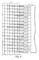
- Figure 3b shows the arrangement of the address decoders determined in Figure 3b according to the present invention in a corresponding manner to Figure 1.
- Figure 5 shows the values representative of the average propagation delay for each address line of Figure 4 in a similar manner to that of Figure 2b. It can be seen that the values indicative of average propagation delay for each address line are not only equal to each other with a value of 60, but also this value is equal to the average value of any pair of true and complementary address lines as previously noted with reference to figure 2b.
- Figure 6a shows the equivalent three-dimensional karnaugh map representation for a six bit address word.
- the x-axis of the map shown in Figure 6a represents the two most significant bits of the address word, a 5 a 4
- the y-axis represents the next two most significant bits, a 3 a 2 .
- a-axis represents the least two significant bits of the address word a 1 a 0 , which are denoted bit pair 3.
- Figures 6b-6e represent the two-dimensional karnaugh maps for each different level of the three-dimensional karnaugh map shown in Figure 4a. Each level represents a different value of bit pair 3. For a six bit address word the required operations to be conducted on the address words must change five of the six bits in the address words. From Figure 6b-6e it can be seen that there are three such operations, the operation shown in Figure 6e being in fact the inverse of that shown in Figure 6b and is therefore not of interest.
- the operations labelled as A, B and C in Figures 6c and 6d can be described as follows;
- sequence of operations required to produce the sequence of address decoders where the address word corresponding to each address decoder alternates five bits at a time is as follows: - perform operation A unless the word address repeats in which case perform a single operation B and resume operation A. Repeat this unless the address word repeats for both an operation A or an operation B, in which case perform a single operation C.
- FIG. 7 which shows the first twenty terms of the sequence for address words for a six bit address word, starting at address word 000000, it can be seen that the sequence of operations falls into groups of four.
- the first four operations are themselves regarded as the first of a group and it can be seen that this group repeats after every four sets of four operations. That is to say, operation C is performed every sixteenth operation.
- the sequence can be readily implemented in a software program using nested loops of operations, or in hardware by the use of an appropriately clocked FIFO or flip flops.
- the value representing the average propagation delay for each of the address lines a 5 to a 0 is calculated as previously shown in Appendices 1 and 2, the value obtained is 1,008 for each address line, as compared to a value of 1,520 for address line a 5 when the decoders are arranged in an ordered sequential fashion. This represents a reduction in average propagation delay of approximately one third.
- K is defined as any integer between 1 and n-1, then the sequence of operations can be denoted as follows: - every 4K operations perform an operation (K+1), otherwise perform an operation 1, where K increments from 1 to (n-1).
- the above analysis results in an ordering of the address decoders for the word lines where the average address line propagation delay is minimised.
- the average propagation delay for the address lines is reduced and thus the speed at which the memory array can be addressed is correspondingly increased.
- the average propagation delay values for the address lines are equal, the timing of various signals applied to the address decoders can be more easily determined.
Landscapes
- Engineering & Computer Science (AREA)
- Microelectronics & Electronic Packaging (AREA)
- Theoretical Computer Science (AREA)
- Dram (AREA)
- Static Random-Access Memory (AREA)
Abstract
Description
- perform operation A unless the word address repeats in which case perform a single operation B and resume operation A. Repeat this unless the address word repeats for both an operation A or an operation B, in which case perform a single operation C.
- every 4K operations perform an operation (K+1), otherwise perform an
Claims (9)
- An integrated circuit memory comprising:a plurality of storage elements arranged in rows and columns;a plurality of word lines, each word line connected to a respective row of storage elements and being connected to a respective address decoder;a plurality of address lines extending from address circuitry to said address decoders, each address decoder being connected to a certain combination of said address lines representing a certain address value to which the address decoder responds to assert its associated word line, wherein said address decoders are connected to said address lines in a manner such that only one of said address lines is connected to adjacent ones of said address decoders.
- An integrated circuit memory according to claim 1, wherein said address decoders are connected to said address lines such that the average propagation delay of said address lines is substantially equal.
- An integrated circuit memory according to any preceding claim, wherein the address lines are organised in pairs, each pair having a true address line and a complementary address line.
- An integrated circuit memory according to any preceding claim, wherein said address lines extend substantially perpendicular to said word lines.
- An integrated circuit memory according to claim 1, wherein the address decoders are connected such that all address lines except one are alternated between successive decoders.
- A method of manufacturing an integrated circuit memory comprising: a plurality of storage elements arranged in rows and columns; a plurality of word lines, each word line connected to a respective row of storage elements and being connected to a respective address decoder; and a plurality of address lines extending from address circuitry to said address decoders, the method comprising:
connecting each of said address decoders to a certain combination of address lines representing a certain address value to which that address decoder responds, wherein said connecting step is carried out so as to connect only one of said address lines to adjacent ones of the address decoders. - A method according to claim 6, which comprises the step of determining the average propagation delay for the address lines prior to implementing the connecting step.
- A method of manufacturing an integrated circuit memory according to claim 7, wherein said address decoders are connected whereby the average propagation delay of said address lines is substantially equal.
- A method of determining the connections between a plurality of address decoders and a plurality of address lines in a memory array, said method comprising:denoting n pairs of address bits, wherein the nth pair of address bits are the least significant bits of an address word;defining n operations of said n pairs of address bits, each operation changing the value of the address word when performed on said address word, wherein each Kth operation, where K is an integer between 1 and n, comprises incrementing the Kth pair of address bits by one term of a 2 bit Gray code and inverting the remaining pairs of address bits;performing said n operations in a predetermined sequence wherein operation (K+1) is performed every 4K operations, otherwise operation 1 is performed, where K increments from 1 to (n-1), whereby a sequence of address words is generated wherein only a single bit has the same value for adjacent address words in said generated sequence of address words.
Applications Claiming Priority (2)
| Application Number | Priority Date | Filing Date | Title |
|---|---|---|---|
| GBGB9929372.2A GB9929372D0 (en) | 1999-12-10 | 1999-12-10 | Address decoder optimization |
| GB9929372 | 1999-12-10 |
Publications (3)
| Publication Number | Publication Date |
|---|---|
| EP1119003A2 true EP1119003A2 (en) | 2001-07-25 |
| EP1119003A3 EP1119003A3 (en) | 2001-09-12 |
| EP1119003B1 EP1119003B1 (en) | 2007-03-07 |
Family
ID=10866172
Family Applications (1)
| Application Number | Title | Priority Date | Filing Date |
|---|---|---|---|
| EP00309493A Expired - Lifetime EP1119003B1 (en) | 1999-12-10 | 2000-10-27 | Address decoder optimization |
Country Status (4)
| Country | Link |
|---|---|
| US (1) | US6529396B2 (en) |
| EP (1) | EP1119003B1 (en) |
| DE (1) | DE60033781D1 (en) |
| GB (1) | GB9929372D0 (en) |
Families Citing this family (2)
| Publication number | Priority date | Publication date | Assignee | Title |
|---|---|---|---|---|
| KR100631929B1 (en) * | 2005-02-15 | 2006-10-04 | 삼성전자주식회사 | Semiconductor Memory Device with Signal Delay Control |
| US7764568B2 (en) * | 2007-07-03 | 2010-07-27 | Seth Lloyd | Bucket brigade address decoding architecture for classical and quantum random access memories |
Family Cites Families (2)
| Publication number | Priority date | Publication date | Assignee | Title |
|---|---|---|---|---|
| EP0520650A1 (en) * | 1991-06-19 | 1992-12-30 | AT&T Corp. | Low power signaling using gray codes |
| US5784330A (en) * | 1996-12-02 | 1998-07-21 | International Business Machines Corporation | Evenly distributed RC delay word line decoding and mapping |
-
1999
- 1999-12-10 GB GBGB9929372.2A patent/GB9929372D0/en not_active Ceased
-
2000
- 2000-10-27 EP EP00309493A patent/EP1119003B1/en not_active Expired - Lifetime
- 2000-10-27 DE DE60033781T patent/DE60033781D1/en not_active Expired - Lifetime
- 2000-12-05 US US09/730,521 patent/US6529396B2/en not_active Expired - Lifetime
Also Published As
| Publication number | Publication date |
|---|---|
| US20010036111A1 (en) | 2001-11-01 |
| US6529396B2 (en) | 2003-03-04 |
| GB9929372D0 (en) | 2000-02-09 |
| DE60033781D1 (en) | 2007-04-19 |
| EP1119003B1 (en) | 2007-03-07 |
| EP1119003A3 (en) | 2001-09-12 |
Similar Documents
| Publication | Publication Date | Title |
|---|---|---|
| US5912854A (en) | Data processing system arranged for operating synchronously with a high speed memory | |
| USRE40932E1 (en) | Content addressable memory (CAM) devices that perform pipelined multi-cycle look-up operations using cam sub-arrays and longest match detection | |
| US4845664A (en) | On-chip bit reordering structure | |
| US4964078A (en) | Combined multiple memories | |
| EP0047842A2 (en) | Skewed matrix address generator | |
| US4773049A (en) | Semiconductor memory device having improved access time for continuously accessing data | |
| CN1009682B (en) | Semiconductor memory | |
| EP0107203B1 (en) | Method of and device for storing three-dimensional digital signals subjected to orthogonal transformation | |
| KR910002202B1 (en) | Boundary-free conductor | |
| CN1215287A (en) | Data transposition system | |
| US4903242A (en) | Serial access memory circuit with improved serial addressing circuit composed of a shift register | |
| CN1253335A (en) | Hardware rotation of image on computer display unit | |
| US6175665B1 (en) | Image inquiry circuit capable of comparing reference image and retrieval object image | |
| JP4808318B2 (en) | Hybrid data I/O data transfer method for memory applications - Patents.com | |
| EP1119003B1 (en) | Address decoder optimization | |
| US8392673B1 (en) | Data writing/reading method, a de-interleaving method, a data processing method, a memory and a memory drive apparatus | |
| KR0167296B1 (en) | Memory Word Line Driver Circuit | |
| EP1481319B1 (en) | Method and apparatus for parallel access to multiple memory modules | |
| Ford | Irreducible representations of the alternating group in odd characteristic | |
| EP0743649B1 (en) | Serial access memory with reduced loop-line delay | |
| EP0393820B1 (en) | Serial dynamic memory shift register | |
| US7093051B2 (en) | Dynamic input/output: configurable data bus for optimizing data throughput | |
| US4677436A (en) | Expandable electronic matrix | |
| EP0624838B1 (en) | Apparatus and method for deinterleaving | |
| SU1241259A1 (en) | Multidimensional statistical analyzer |
Legal Events
| Date | Code | Title | Description |
|---|---|---|---|
| PUAI | Public reference made under article 153(3) epc to a published international application that has entered the european phase |
Free format text: ORIGINAL CODE: 0009012 |
|
| AK | Designated contracting states |
Kind code of ref document: A2 Designated state(s): AT BE CH CY DE DK ES FI FR GB GR IE IT LI LU MC NL PT SE Kind code of ref document: A2 Designated state(s): DE FR GB IT |
|
| AX | Request for extension of the european patent |
Free format text: AL;LT;LV;MK;RO;SI |
|
| PUAL | Search report despatched |
Free format text: ORIGINAL CODE: 0009013 |
|
| AK | Designated contracting states |
Kind code of ref document: A3 Designated state(s): AT BE CH CY DE DK ES FI FR GB GR IE IT LI LU MC NL PT SE |
|
| AX | Request for extension of the european patent |
Free format text: AL;LT;LV;MK;RO;SI |
|
| RIC1 | Information provided on ipc code assigned before grant |
Free format text: 7G 11C 8/00 A, 7H 03M 7/16 B, 7G 11C 5/06 B |
|
| 17P | Request for examination filed |
Effective date: 20020311 |
|
| AKX | Designation fees paid |
Free format text: DE FR GB IT |
|
| GRAP | Despatch of communication of intention to grant a patent |
Free format text: ORIGINAL CODE: EPIDOSNIGR1 |
|
| GRAS | Grant fee paid |
Free format text: ORIGINAL CODE: EPIDOSNIGR3 |
|
| GRAA | (expected) grant |
Free format text: ORIGINAL CODE: 0009210 |
|
| AK | Designated contracting states |
Kind code of ref document: B1 Designated state(s): DE FR GB IT |
|
| REG | Reference to a national code |
Ref country code: GB Ref legal event code: FG4D |
|
| RIN1 | Information on inventor provided before grant (corrected) |
Inventor name: HAMMOND, PAUL |
|
| REF | Corresponds to: |
Ref document number: 60033781 Country of ref document: DE Date of ref document: 20070419 Kind code of ref document: P |
|
| ET | Fr: translation filed | ||
| PGFP | Annual fee paid to national office [announced via postgrant information from national office to epo] |
Ref country code: GB Payment date: 20070925 Year of fee payment: 8 |
|
| PLBE | No opposition filed within time limit |
Free format text: ORIGINAL CODE: 0009261 |
|
| STAA | Information on the status of an ep patent application or granted ep patent |
Free format text: STATUS: NO OPPOSITION FILED WITHIN TIME LIMIT |
|
| PG25 | Lapsed in a contracting state [announced via postgrant information from national office to epo] |
Ref country code: DE Free format text: LAPSE BECAUSE OF FAILURE TO SUBMIT A TRANSLATION OF THE DESCRIPTION OR TO PAY THE FEE WITHIN THE PRESCRIBED TIME-LIMIT Effective date: 20070609 |
|
| 26N | No opposition filed |
Effective date: 20071210 |
|
| PG25 | Lapsed in a contracting state [announced via postgrant information from national office to epo] |
Ref country code: IT Free format text: LAPSE BECAUSE OF FAILURE TO SUBMIT A TRANSLATION OF THE DESCRIPTION OR TO PAY THE FEE WITHIN THE PRESCRIBED TIME-LIMIT Effective date: 20070307 |
|
| PGFP | Annual fee paid to national office [announced via postgrant information from national office to epo] |
Ref country code: FR Payment date: 20071030 Year of fee payment: 8 |
|
| GBPC | Gb: european patent ceased through non-payment of renewal fee |
Effective date: 20081027 |
|
| REG | Reference to a national code |
Ref country code: FR Ref legal event code: ST Effective date: 20090630 |
|
| PG25 | Lapsed in a contracting state [announced via postgrant information from national office to epo] |
Ref country code: FR Free format text: LAPSE BECAUSE OF NON-PAYMENT OF DUE FEES Effective date: 20081031 |
|
| PG25 | Lapsed in a contracting state [announced via postgrant information from national office to epo] |
Ref country code: GB Free format text: LAPSE BECAUSE OF NON-PAYMENT OF DUE FEES Effective date: 20081027 |