EP1117217B1 - A frequency sensitive inductance device for POTS splitter design - Google Patents
A frequency sensitive inductance device for POTS splitter design Download PDFInfo
- Publication number
- EP1117217B1 EP1117217B1 EP01100749A EP01100749A EP1117217B1 EP 1117217 B1 EP1117217 B1 EP 1117217B1 EP 01100749 A EP01100749 A EP 01100749A EP 01100749 A EP01100749 A EP 01100749A EP 1117217 B1 EP1117217 B1 EP 1117217B1
- Authority
- EP
- European Patent Office
- Prior art keywords
- stage
- circuit
- outputs
- inductor
- inputs
- Prior art date
- Legal status (The legal status is an assumption and is not a legal conclusion. Google has not performed a legal analysis and makes no representation as to the accuracy of the status listed.)
- Expired - Lifetime
Links
- 239000003990 capacitor Substances 0.000 claims 7
- 238000003780 insertion Methods 0.000 abstract description 3
- 230000037431 insertion Effects 0.000 abstract description 3
- 230000001939 inductive effect Effects 0.000 description 4
- 230000000694 effects Effects 0.000 description 1
- 230000002452 interceptive effect Effects 0.000 description 1
- 230000009022 nonlinear effect Effects 0.000 description 1
- 230000001151 other effect Effects 0.000 description 1
- 230000009466 transformation Effects 0.000 description 1
- 238000004804 winding Methods 0.000 description 1
Images

Classifications
-
- H—ELECTRICITY
- H04—ELECTRIC COMMUNICATION TECHNIQUE
- H04L—TRANSMISSION OF DIGITAL INFORMATION, e.g. TELEGRAPHIC COMMUNICATION
- H04L27/00—Modulated-carrier systems
- H04L27/0002—Modulated-carrier systems analog front ends; means for connecting modulators, demodulators or transceivers to a transmission line
-
- H—ELECTRICITY
- H03—ELECTRONIC CIRCUITRY
- H03H—IMPEDANCE NETWORKS, e.g. RESONANT CIRCUITS; RESONATORS
- H03H7/00—Multiple-port networks comprising only passive electrical elements as network components
- H03H7/42—Networks for transforming balanced signals into unbalanced signals and vice versa, e.g. baluns
- H03H7/425—Balance-balance networks
- H03H7/427—Common-mode filters
Definitions
- the present invention generally relates to improved telecommunications systems and in particular to an improved digital/POTS telecommunications system. Still more particularly, the present invention relates to an improved digital/POTS splitter design.
- ADSL and VDSL Splitter Design and Telephony Performance show a number of prior art ADSL splitters, which can be either passive or active.
- POTS splitter The basic functions and requirements for POTS Splitter are well defined in TIE 1.4/98-007R5, Annex E.
- POTS splitter is used to split "Plain Old Telephone System” (POTS) voiceband signals from Asymmetric Digital Subscriber Line (ADSL) signals traveling over the same telephone line.
- POTS Packet Old Telephone System
- the POTS splitter is designed as a LC low-pass filter.
- a low-pass filter provides protection from the highfrequency transients and impedance effects that occur during POTS operation, e.g. , ringing transients, ring trip transients, and off-hook transients and impedance changes.
- the low-pass filter provides protection from ADSL signals which may impact through non-linear or other effects remote devices, e.g. , handset, fax, voice band modem, etc., and central office operation.
- Annex E specifies acceptable ranges for insertion loss in the voice band, return loss in the voice band, and attenuation distortion in the ADSL band, among other requirements. These requirements make the common POTS splitter design, which incorporates a differential pair of conventional LC low-pass filter circuits, less than ideal for this purpose. Because the inductor used in a conventional LC low-pass filter circuit is frequency independent in the voice range, it is very hard to meet each of the above requirements at the same time. It would therefore be desirable to provide an improved low-pass filter circuit for a POTS splitter which optimizes the TIE1.4 requirements.
- the POTS splitter design of the preferred embodiment incorporates a low-pass filter which improves the voice-band return loss characteristics without sacrificing performance with regard to the voice-band insertion loss or the ADSL-band attenuation distortion. This is accomplished by replacing the inductor of the conventional POTS splitter low-pass circuit with a parallel-connected inductor and resistor.
- an improved low-pass filter circuit for a POTS splitter which uses a parallel-connected resistor R and inductor L .
- This invention is used to get lower inductive impedance at high frequency (3KHz-4KHz), so a better return loss is obtained without interfering with other performance characteristics.
- Figure 1 shows the basic structure of this invention.
- Equation 2 The imaginary part if the impedance is (Equation 2):
- FIG. 2 shows a POTS splitter device, in accordance with the preferred embodiment, which incorporates a low-pass filter with the improved inductor circuit described above.
- transformers are used as differential mode inductors.
- the transformer TX1 is shown with each inductive coil connected in parallel with a respective resistor R1 and R2 .
- this is merely exemplary; according to different requirements for the central office and remote end POTS splitters, the value of R and L may change in different designs.
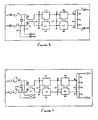
- FIGs 3 and 4 respectively, show POTS splitter designs, using frequency-sensitive inductance devices in accordance with the preferred embodiment, of a central office POTS splitter and a remote end POTS splitter.
- the frequency sensitive device consists of L3, R2, and R3.
- the low-pass filter is therefore comprised of L3, R2, R3, and C4 in Figure 3, and L3, R2, R3, and C3 in Figure 4.
- Other parts of the circuit will be understood by those of skill in the art as a conventional POTS splitter circuit.
- stage 1 the conventional circuit comprised by L1 and C2 in Figure 3, and by L1 and C1 in Figure 4, will be referred to as "stage 1" of each of these figures.
- stage 2 the conventional circuit comprised by L2, C5, C6 , and C3 in Figure 3, and by L2, C5, C6, and C2 in Figure 4, will be referred to as "stage 2" of each of these figures.
- stage 3 will reference the frequency-sensitive circuit of the preferred embodiment, which comprises L3, R2, R3, and C4 in Figure 3, and by L3 , R2, R3 , and C3 in Figure 4.
- nodes A and B form the inputs to stage 1
- nodes C and D are both the outputs of stage 1 and the inputs of stage 2.
- nodes E and F are both the outputs of stage 2 and the inputs of stage 3
- nodes G and H are the outputs of stage 3.
- a combined voice-band and ADSL signal is received by the splitter circuits at inputs L1T and L1R of Figure 3, and inputs LT and LR of Figure 4.
- the ADSL signal is output at outputs D1T and D1R of Figure 3, and outputs DT and DR of Figure 4.
- the ADSL signal is filtered from the voiceband signal, and the voiceband signal is output at outputs V1T and V1R of Figure 3, and outputs VT and VR of Figure 4.
- the values of the components of Figure 3 are as follows: L1 20 mH ( ⁇ 8%) L2, L3 12 mH ( ⁇ 8%) C11, C12 120 nF 400V ( ⁇ 10%) C2 10 nF 400V ( ⁇ 5%) C3 10 nF 400V ( ⁇ 5%) C4 47 nF 400V ( ⁇ 5%) C5, C6 4.7 nF 400V ( ⁇ 5%) R2, R3 200
- the values of the components of Figure 4 are as follows: L1 20 mH ( ⁇ 8%) L2, L3 12 mH ( ⁇ 8%) C1 33 nF 400V ( ⁇ 5%) C2 22 nF 400V ( ⁇ 5%) C3 47 nF 400V ( ⁇ 5%) C4 0.47 nF 400V ( ⁇ 5%) C5, C6 4.7 nF 400V ( ⁇ 5%) R1 33.1K 1% .25W R2, R3 100 10% .25W
- the preferred frequency sensitive device that consists of L3, R2, and R3, from stage 3, can be used to replace other conventional transformer/filter circuits, e . g ., the C5, C6, L2 circuit of stage 2. This means that a frequency-sensitive circuit as in stage 3 may also appear as the first or second stage.
- the position of the frequency-sensitive inductive device within the POTS splitter will vary the overall performance characteristics of the splitter.
- the stage 3 circuit can be switched with the stage 2 circuit, so that their order is reversed, according to the requirements of the system in which the system is to be installed.
- the preferred embodiment by incorporating this frequency-sensitive inductive device, will simultaneously minimize the magnitude of ripple in the high frequency band (3K-4KHz) and maximize the return loss at high frequency band (3K-4KHz), without negatively affecting, to any substantial degree, the attenuation distortion of the ADSL band.
Landscapes
- Engineering & Computer Science (AREA)
- Computer Networks & Wireless Communication (AREA)
- Signal Processing (AREA)
- Filters And Equalizers (AREA)
- Networks Using Active Elements (AREA)
- Coils Or Transformers For Communication (AREA)
- Use Of Switch Circuits For Exchanges And Methods Of Control Of Multiplex Exchanges (AREA)
Abstract
Description
- The present invention generally relates to improved telecommunications systems and in particular to an improved digital/POTS telecommunications system. Still more particularly, the present invention relates to an improved digital/POTS splitter design.
- The paper "ADSL and VDSL Splitter Design and Telephony Performance", by J. Lock and P. Sheppard shows a number of prior art ADSL splitters, which can be either passive or active.
- The basic functions and requirements for POTS Splitter are well defined in TIE 1.4/98-007R5, Annex E. The POTS splitter is used to split "Plain Old Telephone System" (POTS) voiceband signals from Asymmetric Digital Subscriber Line (ADSL) signals traveling over the same telephone line.
- In conventional systems, the POTS splitter is designed as a LC low-pass filter. With regard to ADSL signals, a low-pass filter provides protection from the highfrequency transients and impedance effects that occur during POTS operation, e.g., ringing transients, ring trip transients, and off-hook transients and impedance changes. With regard to POTS voice band service, the low-pass filter provides protection from ADSL signals which may impact through non-linear or other effects remote devices, e.g., handset, fax, voice band modem, etc., and central office operation.
- TIE1.4/98-007R5, Annex E specifies acceptable ranges for insertion loss in the voice band, return loss in the voice band, and attenuation distortion in the ADSL band, among other requirements. These requirements make the common POTS splitter design, which incorporates a differential pair of conventional LC low-pass filter circuits, less than ideal for this purpose. Because the inductor used in a conventional LC low-pass filter circuit is frequency independent in the voice range, it is very hard to meet each of the above requirements at the same time. It would therefore be desirable to provide an improved low-pass filter circuit for a POTS splitter which optimizes the TIE1.4 requirements.
- The POTS splitter design of the preferred embodiment incorporates a low-pass filter which improves the voice-band return loss characteristics without sacrificing performance with regard to the voice-band insertion loss or the ADSL-band attenuation distortion. This is accomplished by replacing the inductor of the conventional POTS splitter low-pass circuit with a parallel-connected inductor and resistor.
-
- Figure 1 depicts a basic RL inductor circuit in accordance with a preferred embodiment of the present invention;
- Figure 2 depicts a differential-mode RL inductor pair in accordance with a preferred embodiment of the present invention;
- Figure 3 depicts a central-office POTS splitter employing a low-pass filter circuit in accordance with a preferred embodiment of the present invention; and
- Figure 4 depicts a remote-end POTS splitter employing a low-pass filter circuit in accordance with a preferred embodiment of the present invention.
-
- With reference now to the figures, and in particular with reference to Figure 1, there is provided an improved low-pass filter circuit for a POTS splitter, which uses a parallel-connected resistor R and inductor L.
- This invention is used to get lower inductive impedance at high frequency (3KHz-4KHz), so a better return loss is obtained without interfering with other performance characteristics.
- Figure 1 shows the basic structure of this invention. The total impedance of this device is (Equation 1):

- As the frequency goes high,
- Figure 2 shows a POTS splitter device, in accordance with the preferred embodiment, which incorporates a low-pass filter with the improved inductor circuit described above. In the POTS splitter, transformers are used as differential mode inductors. In Figure 2, the transformer TX1 is shown with each inductive coil connected in parallel with a respective resistor R1 and R2. The impedance of each side of transformer TX1 is described by Equations 1 and 2, above; the transformation from Figure 1 to Figure 2 is:
- Figures 3 and 4, respectively, show POTS splitter designs, using frequency-sensitive inductance devices in accordance with the preferred embodiment, of a central office POTS splitter and a remote end POTS splitter. In these figures, the frequency sensitive device consists of L3, R2, and R3. The low-pass filter is therefore comprised of L3, R2, R3, and C4 in Figure 3, and L3, R2, R3, and C3 in Figure 4. Other parts of the circuit will be understood by those of skill in the art as a conventional POTS splitter circuit.
- For purposes of this discussion, the conventional circuit comprised by L1 and C2 in Figure 3, and by L1 and C1 in Figure 4, will be referred to as "stage 1" of each of these figures. Similarly, the conventional circuit comprised by L2, C5, C6, and C3 in Figure 3, and by L2, C5, C6, and C2 in Figure 4, will be referred to as "stage 2" of each of these figures. Finally, "stage 3" will reference the frequency-sensitive circuit of the preferred embodiment, which comprises L3, R2, R3, and C4 in Figure 3, and by L3, R2, R3, and C3 in Figure 4.
- It will then been clear that, in Figures 3 and 4, nodes A and B form the inputs to stage 1, and nodes C and D are both the outputs of stage 1 and the inputs of stage 2. Nodes E and F are both the outputs of stage 2 and the inputs of stage 3, and nodes G and H are the outputs of stage 3.
- In normal operation, a combined voice-band and ADSL signal is received by the splitter circuits at inputs L1T and L1R of Figure 3, and inputs LT and LR of Figure 4. The ADSL signal is output at outputs D1T and D1R of Figure 3, and outputs DT and DR of Figure 4. The ADSL signal is filtered from the voiceband signal, and the voiceband signal is output at outputs V1T and V1R of Figure 3, and outputs VT and VR of Figure 4.
- According to the preferred embodiment, the values of the components of Figure 3 are as follows:
L1 20 mH (±8%) L2, L3 12 mH (±8%) C11, C12 120 nF 400V (±10%) C2 10 nF 400V (±5%) C3 10 nF 400V (±5%) C4 47 nF 400V (±5%) C5, C6 4.7 nF 400V (±5%) R2, R3 200 - Also according to the preferred embodiment, the values of the components of Figure 4 are as follows:
L1 20 mH (±8%) L2, L3 12 mH (±8%) C1 33 nF 400V (±5%) C2 22 nF 400V (±5%) C3 47 nF 400V (±5%) C4 0.47 nF 400V (±5%) C5, C6 4.7 nF 400V (±5%) R1 33.1K 1% .25W R2, R3 100 10% .25W - Of course, while the component values of the preferred embodiment are shown above, those of skill in the art will recognize that these values can be varied according to specific system requirements. In particular, in Figure 3 and Figure 4, the preferred frequency sensitive device that consists of L3, R2, and R3, from stage 3, can be used to replace other conventional transformer/filter circuits, e.g., the C5, C6, L2 circuit of stage 2. This means that a frequency-sensitive circuit as in stage 3 may also appear as the first or second stage.
- Further, the position of the frequency-sensitive inductive device within the POTS splitter will vary the overall performance characteristics of the splitter. For example, in Figure 4 above, the stage 3 circuit can be switched with the stage 2 circuit, so that their order is reversed, according to the requirements of the system in which the system is to be installed.
- The preferred embodiment, by incorporating this frequency-sensitive inductive device, will simultaneously minimize the magnitude of ripple in the high frequency band (3K-4KHz) and maximize the return loss at high frequency band (3K-4KHz), without negatively affecting, to any substantial degree, the attenuation distortion of the ADSL band.
- While the invention has been particularly shown and described with reference to a preferred embodiment, it will be understood by those skilled in the art that various changes in form and detail may be made.
Claims (7)
- An electrical splitter circuit, comprising:a first stage (E, F, G, H) having first (E) and second (F) inputs and first (G) and second (H) outputs, the first stage comprising:a parallel-connected first inductor and first resistor, connected between the first input (E) and first output (G),a parallel-connected second inductor and second resistor, connected between the second input (F) and second output (H), the first and second inductors being inductively coupled, anda capacitor (C4, C3) connected between the first (G) and second (H) outputs.
- The circuit of claim 1, further comprising:wherein the first and second outputs (E, F) of the second stage are operatively connected to the first and second inputs (E, F) of the first stage, respectively.a second stage (C,D,E,F) having first (C) and second (D) inputs and first (E) and second (F) outputs, the second stage comprisinga parallel-connected first inductor and first capacitor (C5), connected between the first input (C) and first output (E),a parallel-connected second inductor and second capacitor (C6), connected between the second input (D) and second output (F), the first and second inductors being inductively coupled, anda third capacitor (C3, C2) connected between the first (E) and second (F) outputs of the second stage,
- The circuit of claim 1 or 2, further comprising:wherein the first and second outputs (C, D) of the third stage are operatively connected to the first and second inputs (E, F) of the first stage, respectively.a third stage (A,B,C,D) having first (A) and second (B) inputs and first (C) and second (D) outputs, the third stage comprisinga first inductor connected between the first input (A) and first output (C),a second inductor connected between the second input (B) and second output (D), the first and second inductors being inductively coupled, anda capacitor (C2, C1) connected between the first and second outputs (C, D) of the third stage,
- The circuit of any one of claims 1 to 3, wherein a signal carrying both voice and data information is received at the first and second inputs of the first stage (E, F).
- The circuit of any one of claims 1 to 4, wherein the circuit filters a lower-frequency portion of a signal received at the first and second inputs of the first stage (E, F).
- The circuit of any one of claims 1 to 5, wherein the circuit reduces the distortion of a signal received at the first and second inputs of the first stage and delivered at the first and second outputs of the respective outputs.
- The circuit of claim 1, further comprising a third output (D1T), connected via a second capacitor (C12) to the first input (A) of the third stage, and a fourth output (D1R), connected via a third capacitor (C11) to the second input (B) of the third stage.
Applications Claiming Priority (2)
| Application Number | Priority Date | Filing Date | Title |
|---|---|---|---|
| US483756 | 1974-06-27 | ||
| US09/483,756 US7020276B1 (en) | 2000-01-14 | 2000-01-14 | Frequency sensitive inductance device in POTS splitter design |
Publications (3)
| Publication Number | Publication Date |
|---|---|
| EP1117217A2 EP1117217A2 (en) | 2001-07-18 |
| EP1117217A3 EP1117217A3 (en) | 2004-06-09 |
| EP1117217B1 true EP1117217B1 (en) | 2005-07-13 |
Family
ID=23921400
Family Applications (1)
| Application Number | Title | Priority Date | Filing Date |
|---|---|---|---|
| EP01100749A Expired - Lifetime EP1117217B1 (en) | 2000-01-14 | 2001-01-12 | A frequency sensitive inductance device for POTS splitter design |
Country Status (8)
| Country | Link |
|---|---|
| US (1) | US7020276B1 (en) |
| EP (1) | EP1117217B1 (en) |
| JP (1) | JP2001251155A (en) |
| AT (1) | ATE299634T1 (en) |
| BR (1) | BR0100266A (en) |
| CA (1) | CA2326929C (en) |
| DE (1) | DE60111873T2 (en) |
| ES (1) | ES2245328T3 (en) |
Families Citing this family (5)
| Publication number | Priority date | Publication date | Assignee | Title |
|---|---|---|---|---|
| US6895089B2 (en) * | 2001-12-14 | 2005-05-17 | Adc Dsl Systems, Inc. | Pots splitter with line impedance matching |
| US6853724B2 (en) | 2001-12-14 | 2005-02-08 | Adc Dsl Systems, Inc. | Cascade low-pass filter to improve xDSL band attenuation for POTS splitter |
| JP2003309443A (en) * | 2002-04-15 | 2003-10-31 | Nippon Telegraph & Telephone East Corp | Line noise filter |
| JP4767025B2 (en) * | 2006-01-25 | 2011-09-07 | 株式会社オートネットワーク技術研究所 | Branch connector |
| JP5994108B2 (en) * | 2012-11-27 | 2016-09-21 | パナソニックIpマネジメント株式会社 | Common mode noise filter |
Family Cites Families (5)
| Publication number | Priority date | Publication date | Assignee | Title |
|---|---|---|---|---|
| US5848150A (en) * | 1997-02-26 | 1998-12-08 | Paradyne Corporation | Passive distributed filter system and method |
| EP0942578A3 (en) * | 1998-03-12 | 2002-01-30 | Westell Technologies, Inc. | Dual-mode filter for ADSL |
| ES2271983T3 (en) * | 1998-06-26 | 2007-04-16 | Alcatel | PROVISION OF FILTER APPLICABLE TO ADSL SIGNAL SEPARATORS. |
| US6567519B1 (en) * | 1999-05-28 | 2003-05-20 | Cisco Technology, Inc. | System and method for processing an input signal communicated on a telephone line |
| US6137880A (en) * | 1999-08-27 | 2000-10-24 | Westell Technologies, Inc. | Passive splitter filter for digital subscriber line voice communication for complex impedance terminations |
-
2000
- 2000-01-14 US US09/483,756 patent/US7020276B1/en not_active Expired - Lifetime
- 2000-11-28 CA CA002326929A patent/CA2326929C/en not_active Expired - Lifetime
-
2001
- 2001-01-10 BR BR0100266-0A patent/BR0100266A/en not_active IP Right Cessation
- 2001-01-12 JP JP2001005028A patent/JP2001251155A/en active Pending
- 2001-01-12 ES ES01100749T patent/ES2245328T3/en not_active Expired - Lifetime
- 2001-01-12 AT AT01100749T patent/ATE299634T1/en not_active IP Right Cessation
- 2001-01-12 DE DE60111873T patent/DE60111873T2/en not_active Expired - Lifetime
- 2001-01-12 EP EP01100749A patent/EP1117217B1/en not_active Expired - Lifetime
Also Published As
| Publication number | Publication date |
|---|---|
| US7020276B1 (en) | 2006-03-28 |
| CA2326929A1 (en) | 2001-07-14 |
| CA2326929C (en) | 2009-04-14 |
| ES2245328T3 (en) | 2006-01-01 |
| EP1117217A3 (en) | 2004-06-09 |
| DE60111873D1 (en) | 2005-08-18 |
| EP1117217A2 (en) | 2001-07-18 |
| ATE299634T1 (en) | 2005-07-15 |
| DE60111873T2 (en) | 2006-04-20 |
| JP2001251155A (en) | 2001-09-14 |
| BR0100266A (en) | 2001-08-21 |
Similar Documents
| Publication | Publication Date | Title |
|---|---|---|
| CA2182383C (en) | Filtering | |
| US6137880A (en) | Passive splitter filter for digital subscriber line voice communication for complex impedance terminations | |
| US6728367B1 (en) | Apparatus and method for filtering voiceband and metering tone frequencies of a mixed voice/data signal | |
| US6853724B2 (en) | Cascade low-pass filter to improve xDSL band attenuation for POTS splitter | |
| US6895089B2 (en) | Pots splitter with line impedance matching | |
| EP1086575B1 (en) | A method for separating narrowband and broadband services on a transmission link and a splitter element | |
| US6674843B1 (en) | Apparatus system and method for enabling multi-frequency communication over a telephone network having a billing/tax tone | |
| US6804349B1 (en) | Hybrid transceiver circuit | |
| US6856682B1 (en) | System and method for processing an input signal communicated on a telephone line | |
| CN101150303A (en) | Multiple order low pass filter for an xDSL splitter in a telecommunication system | |
| EP1117217A2 (en) | A frequency sensitive inductance device for POTS splitter design | |
| EP1241799A1 (en) | Hybrid circuit for a broadband modem | |
| US6978011B1 (en) | Enhanced low pass filter | |
| WO2000048314A1 (en) | Multiplexing and demultiplexing of narrowband and broadband services in a transmission connection | |
| US7684499B2 (en) | Multi-band line interface circuit with line side cancellation | |
| US6937719B2 (en) | Multiplexing and demultiplexing of narrowband and broadband services in a transmission connection | |
| EP2066103B1 (en) | Switchable impedance xdsl splitter | |
| US8165283B2 (en) | Advanced ADSL splitter | |
| US6483914B1 (en) | Telephone filter arrangement | |
| US6826265B1 (en) | DSL-ready pots device and method | |
| WO1999040716A2 (en) | Active splitter | |
| CA2376137A1 (en) | Highly integrated adsl linecard | |
| KR200328611Y1 (en) | Filter circuit for digital subscriber line | |
| JP2003516674A (en) | ADSL frequency separation network | |
| CA2424855C (en) | Cascade low-pass filter to improve xdsl band attenuation for pots splitter |
Legal Events
| Date | Code | Title | Description |
|---|---|---|---|
| PUAI | Public reference made under article 153(3) epc to a published international application that has entered the european phase |
Free format text: ORIGINAL CODE: 0009012 |
|
| AK | Designated contracting states |
Kind code of ref document: A2 Designated state(s): AT BE CH CY DE DK ES FI FR GB GR IE IT LI LU MC NL PT SE TR |
|
| AX | Request for extension of the european patent |
Free format text: AL;LT;LV;MK;RO;SI |
|
| PUAL | Search report despatched |
Free format text: ORIGINAL CODE: 0009013 |
|
| AK | Designated contracting states |
Kind code of ref document: A3 Designated state(s): AT BE CH CY DE DK ES FI FR GB GR IE IT LI LU MC NL PT SE TR |
|
| AX | Request for extension of the european patent |
Extension state: AL LT LV MK RO SI |
|
| RIC1 | Information provided on ipc code assigned before grant |
Ipc: 7H 03H 7/06 B Ipc: 7H 04L 5/06 B Ipc: 7H 04L 27/00 A Ipc: 7H 03H 7/09 B Ipc: 7H 04L 5/14 B |
|
| 17P | Request for examination filed |
Effective date: 20041009 |
|
| GRAP | Despatch of communication of intention to grant a patent |
Free format text: ORIGINAL CODE: EPIDOSNIGR1 |
|
| AKX | Designation fees paid |
Designated state(s): AT BE CH CY DE DK ES FI FR GB GR IE IT LI LU MC NL PT SE TR |
|
| GRAS | Grant fee paid |
Free format text: ORIGINAL CODE: EPIDOSNIGR3 |
|
| GRAA | (expected) grant |
Free format text: ORIGINAL CODE: 0009210 |
|
| AK | Designated contracting states |
Kind code of ref document: B1 Designated state(s): AT BE CH CY DE DK ES FI FR GB GR IE IT LI LU MC NL PT SE TR |
|
| PG25 | Lapsed in a contracting state [announced via postgrant information from national office to epo] |
Ref country code: IT Free format text: LAPSE BECAUSE OF FAILURE TO SUBMIT A TRANSLATION OF THE DESCRIPTION OR TO PAY THE FEE WITHIN THE PRESCRIBED TIME-LIMIT;WARNING: LAPSES OF ITALIAN PATENTS WITH EFFECTIVE DATE BEFORE 2007 MAY HAVE OCCURRED AT ANY TIME BEFORE 2007. THE CORRECT EFFECTIVE DATE MAY BE DIFFERENT FROM THE ONE RECORDED. Effective date: 20050713 Ref country code: AT Free format text: LAPSE BECAUSE OF FAILURE TO SUBMIT A TRANSLATION OF THE DESCRIPTION OR TO PAY THE FEE WITHIN THE PRESCRIBED TIME-LIMIT Effective date: 20050713 Ref country code: FI Free format text: LAPSE BECAUSE OF FAILURE TO SUBMIT A TRANSLATION OF THE DESCRIPTION OR TO PAY THE FEE WITHIN THE PRESCRIBED TIME-LIMIT Effective date: 20050713 Ref country code: NL Free format text: LAPSE BECAUSE OF FAILURE TO SUBMIT A TRANSLATION OF THE DESCRIPTION OR TO PAY THE FEE WITHIN THE PRESCRIBED TIME-LIMIT Effective date: 20050713 Ref country code: TR Free format text: LAPSE BECAUSE OF FAILURE TO SUBMIT A TRANSLATION OF THE DESCRIPTION OR TO PAY THE FEE WITHIN THE PRESCRIBED TIME-LIMIT Effective date: 20050713 |
|
| REG | Reference to a national code |
Ref country code: GB Ref legal event code: FG4D |
|
| REG | Reference to a national code |
Ref country code: CH Ref legal event code: EP |
|
| REG | Reference to a national code |
Ref country code: IE Ref legal event code: FG4D |
|
| REF | Corresponds to: |
Ref document number: 60111873 Country of ref document: DE Date of ref document: 20050818 Kind code of ref document: P |
|
| PG25 | Lapsed in a contracting state [announced via postgrant information from national office to epo] |
Ref country code: DK Free format text: LAPSE BECAUSE OF FAILURE TO SUBMIT A TRANSLATION OF THE DESCRIPTION OR TO PAY THE FEE WITHIN THE PRESCRIBED TIME-LIMIT Effective date: 20051013 Ref country code: SE Free format text: LAPSE BECAUSE OF FAILURE TO SUBMIT A TRANSLATION OF THE DESCRIPTION OR TO PAY THE FEE WITHIN THE PRESCRIBED TIME-LIMIT Effective date: 20051013 Ref country code: GR Free format text: LAPSE BECAUSE OF FAILURE TO SUBMIT A TRANSLATION OF THE DESCRIPTION OR TO PAY THE FEE WITHIN THE PRESCRIBED TIME-LIMIT Effective date: 20051013 |
|
| REG | Reference to a national code |
Ref country code: CH Ref legal event code: NV Representative=s name: SUSI PRYDE-HAENI BSC |
|
| PG25 | Lapsed in a contracting state [announced via postgrant information from national office to epo] |
Ref country code: PT Free format text: LAPSE BECAUSE OF FAILURE TO SUBMIT A TRANSLATION OF THE DESCRIPTION OR TO PAY THE FEE WITHIN THE PRESCRIBED TIME-LIMIT Effective date: 20051219 |
|
| REG | Reference to a national code |
Ref country code: ES Ref legal event code: FG2A Ref document number: 2245328 Country of ref document: ES Kind code of ref document: T3 |
|
| NLV1 | Nl: lapsed or annulled due to failure to fulfill the requirements of art. 29p and 29m of the patents act | ||
| PG25 | Lapsed in a contracting state [announced via postgrant information from national office to epo] |
Ref country code: GB Free format text: LAPSE BECAUSE OF NON-PAYMENT OF DUE FEES Effective date: 20060112 Ref country code: IE Free format text: LAPSE BECAUSE OF NON-PAYMENT OF DUE FEES Effective date: 20060112 |
|
| PG25 | Lapsed in a contracting state [announced via postgrant information from national office to epo] |
Ref country code: LU Free format text: LAPSE BECAUSE OF NON-PAYMENT OF DUE FEES Effective date: 20060131 Ref country code: MC Free format text: LAPSE BECAUSE OF NON-PAYMENT OF DUE FEES Effective date: 20060131 |
|
| ET | Fr: translation filed | ||
| PLBE | No opposition filed within time limit |
Free format text: ORIGINAL CODE: 0009261 |
|
| STAA | Information on the status of an ep patent application or granted ep patent |
Free format text: STATUS: NO OPPOSITION FILED WITHIN TIME LIMIT |
|
| 26N | No opposition filed |
Effective date: 20060418 |
|
| GBPC | Gb: european patent ceased through non-payment of renewal fee |
Effective date: 20060112 |
|
| REG | Reference to a national code |
Ref country code: IE Ref legal event code: MM4A |
|
| PG25 | Lapsed in a contracting state [announced via postgrant information from national office to epo] |
Ref country code: CY Free format text: LAPSE BECAUSE OF FAILURE TO SUBMIT A TRANSLATION OF THE DESCRIPTION OR TO PAY THE FEE WITHIN THE PRESCRIBED TIME-LIMIT Effective date: 20050713 |
|
| PGFP | Annual fee paid to national office [announced via postgrant information from national office to epo] |
Ref country code: CH Payment date: 20100125 Year of fee payment: 10 Ref country code: ES Payment date: 20100126 Year of fee payment: 10 |
|
| PGFP | Annual fee paid to national office [announced via postgrant information from national office to epo] |
Ref country code: FR Payment date: 20100205 Year of fee payment: 10 |
|
| PGFP | Annual fee paid to national office [announced via postgrant information from national office to epo] |
Ref country code: DE Payment date: 20100127 Year of fee payment: 10 Ref country code: BE Payment date: 20100121 Year of fee payment: 10 |
|
| BERE | Be: lapsed |
Owner name: *CORNING CABLE SYSTEMS LLC Effective date: 20110131 |
|
| REG | Reference to a national code |
Ref country code: CH Ref legal event code: PL |
|
| REG | Reference to a national code |
Ref country code: FR Ref legal event code: ST Effective date: 20110930 |
|
| PG25 | Lapsed in a contracting state [announced via postgrant information from national office to epo] |
Ref country code: LI Free format text: LAPSE BECAUSE OF NON-PAYMENT OF DUE FEES Effective date: 20110131 Ref country code: FR Free format text: LAPSE BECAUSE OF NON-PAYMENT OF DUE FEES Effective date: 20110131 Ref country code: CH Free format text: LAPSE BECAUSE OF NON-PAYMENT OF DUE FEES Effective date: 20110131 |
|
| PG25 | Lapsed in a contracting state [announced via postgrant information from national office to epo] |
Ref country code: BE Free format text: LAPSE BECAUSE OF NON-PAYMENT OF DUE FEES Effective date: 20110131 |
|
| REG | Reference to a national code |
Ref country code: DE Ref legal event code: R119 Ref document number: 60111873 Country of ref document: DE Effective date: 20110802 |
|
| REG | Reference to a national code |
Ref country code: ES Ref legal event code: FD2A Effective date: 20120220 |
|
| PG25 | Lapsed in a contracting state [announced via postgrant information from national office to epo] |
Ref country code: ES Free format text: LAPSE BECAUSE OF NON-PAYMENT OF DUE FEES Effective date: 20110113 |
|
| PG25 | Lapsed in a contracting state [announced via postgrant information from national office to epo] |
Ref country code: DE Free format text: LAPSE BECAUSE OF NON-PAYMENT OF DUE FEES Effective date: 20110802 |