EP1117181A2 - Voltage protection and biasing circuit - Google Patents
Voltage protection and biasing circuit Download PDFInfo
- Publication number
- EP1117181A2 EP1117181A2 EP01300108A EP01300108A EP1117181A2 EP 1117181 A2 EP1117181 A2 EP 1117181A2 EP 01300108 A EP01300108 A EP 01300108A EP 01300108 A EP01300108 A EP 01300108A EP 1117181 A2 EP1117181 A2 EP 1117181A2
- Authority
- EP
- European Patent Office
- Prior art keywords
- voltage
- circuit
- coupled
- component
- transistor
- Prior art date
- Legal status (The legal status is an assumption and is not a legal conclusion. Google has not performed a legal analysis and makes no representation as to the accuracy of the status listed.)
- Granted
Links
Images
Classifications
-
- H—ELECTRICITY
- H03—ELECTRONIC CIRCUITRY
- H03K—PULSE TECHNIQUE
- H03K17/00—Electronic switching or gating, i.e. not by contact-making and –breaking
- H03K17/14—Modifications for compensating variations of physical values, e.g. of temperature
- H03K17/145—Modifications for compensating variations of physical values, e.g. of temperature in field-effect transistor switches
-
- H—ELECTRICITY
- H03—ELECTRONIC CIRCUITRY
- H03K—PULSE TECHNIQUE
- H03K17/00—Electronic switching or gating, i.e. not by contact-making and –breaking
- H03K17/16—Modifications for eliminating interference voltages or currents
- H03K17/161—Modifications for eliminating interference voltages or currents in field-effect transistor switches
- H03K17/162—Modifications for eliminating interference voltages or currents in field-effect transistor switches without feedback from the output circuit to the control circuit
Definitions
- This invention relates to a voltage protection and biasing circuit and more particularly, to a circuit which allows voltage to be provided to a terminal of a transistor, effective to operatively bias the transistor while concomitantly protecting the transistor from damage which is caused by transient voltage surges or "spikes".
- Transistors such as and without limitation field effect transistors
- a device such as a switch
- a field effect transistor to selectively couple and/or communicate the voltage which emanates from the vehicle battery to a component or load, such as an interior convenience lamp or window activation motor.
- the switch or device selectively biases or allows voltage to be applied to the gate terminal of the field effect transistor, effective to allow battery voltage to be communicated to the component or load through the source and drain terminals of the transistor.
- the field effect transistor in this arrangement, is typically biased by use of the vehicle battery (i.e., the battery voltage is selectively applied and/or communicated to the gate terminal of the field effect transistor).
- the biasing voltage damages, destroys, or “punches through” the field effect transistor, thereby requiring repair and replacement of the transistor, undesirably increasing the overall vehicle maintenance costs, and potentially causing surge type damage to the other components of the vehicle.
- the load or component is protected against such "spikes" in one of several conventional and known manners.
- a voltage divider circuit is typically coupled between the vehicle battery and the field effect transistor and is effective to reduce the amount of biasing voltage which is communicated and/or coupled to the gate terminal of the field effect transistor.
- the amount of such voltage reduction is limited by the amount of voltage which is required to be communicated to the field effect transistor in order to operatively bias the transistor.
- this voltage reduction approach and circuit configuration is effective to protect the field effect transistor from some relatively small transient voltage increases or surges, it does not typically provide protection against large transient voltage increases.
- Zener diodes are also connected to the vehicle battery and to the field effect transistor and are somewhat more effective to protect the field effect transistor against transient voltage increases or surges.
- these zener diodes are relatively costly and undesirably increase the overall complexity of the circuit.
- a circuit for use in combination with a battery which is adapted to selectively generate a voltage, a component which is to selectively receive the voltage, and a field effect transistor which has a source terminal which is coupled to the battery, a drain terminal which is coupled to the device, and a gate terminal which selectively allows the voltage to be communicated from the battery to the component through the source and drain terminals.
- the circuit includes a substantially constant electrical current source; and a resistor which is coupled to the substantially constant electrical current source and which cooperates with the substantially constant electrical current source to provide a substantially constant amount of biasing voltage to the field effect transistor.
- a method for allowing electrical voltage to be communicated from a battery to a device, the voltage varying between a first low value and a second higher value.
- the method including the steps of providing an electrical component which allows the electrical power to be communicated from the battery to the device when the electrical component receives an electrical signal having a certain value; creating the electrical signal; communicating the electrical signal to the electrical component; causing the communicated electrical signal to have and maintain the certain value when the voltage varies between the first low value and the second high value.
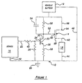
- Figure 1 is a schematic diagram of a biasing and protection circuit which is made in accordance with the teachings of the preferred embodiment of the invention and which is operatively coupled to a vehicle battery and to a component and/or load.
- circuit 10 is operatively coupled to and used in combination with a vehicle battery 12 of the type which selectively generates a voltage signal (i.e., which generates electrical power), a component or load 18 which is to selectively receive the generated voltage signal or electrical power emanating from the vehicle battery 12 by use of an electrical component such as a field effect transistor 14, and a device or switch 16 which selectively activates the component or load 18 (i.e., which causes the voltage signal or electrical power which is generated and which emanates from the battery 12 to be communicated to the component or load 18).
- a voltage signal i.e., which generates electrical power
- a component or load 18 which is to selectively receive the generated voltage signal or electrical power emanating from the vehicle battery 12 by use of an electrical component such as a field effect transistor 14, and a device or switch 16 which selectively activates the component or load 18 (i.e., which causes the voltage signal or electrical power which is generated and which emanates from the battery 12 to be communicated to the component or load 18).
- controller or device 16 selectively generates a voltage signal upon bus 20 having one of two voltage values which, as is more fully delineated below, are typically used to activate or deactivate the component or load 18 (i.e., the term “deactivate” means to substantially prevent the voltage signal and electrical power emanating from the vehicle battery 12 from being communicated to the component or load 18).
- the voltage which is operatively used to operationally activate device 16 i.e., to allow device 16 to operate in the foregoing manner
- battery 12 the voltage which is operatively used to operationally activate device 16 (i.e., to allow device 16 to operate in the foregoing manner) is supplied by battery 12.
- Circuit 10 includes a transistor 22 (i.e., a bi-polar transistor of the p-n-p type) having a base terminal 24 which is coupled to a source of electrical ground potential 26 through resistor 28.
- Transistor 22 further has a collector terminal 30 which is coupled to a resistor 32 and a capacitor 34. Both capacitor 34 and the resistor 32 are coupled to the vehicle battery 12 and are arranged and connected, as should be apparent to those of ordinary skill in the art, in an electrical "parallel" manner or fashion.
- Transistor 22 further includes an emitter terminal 36 which is coupled to the source of electrical ground potential 26 by use of resistor 38.
- Bus 20 is coupled to resistor 28 and to the base terminal 24 by use of resistor 40, and device 16 and component or load 18 are each coupled to the source of electrical ground potential 26 by respective busses 42, 44.
- the vehicle battery 12 is also coupled to the source of electrical ground potential 26 by use of bus 46.
- the gate terminal 50 of the field effect transistor 14 is coupled to the resistor 32 and to the collector terminal 30 by use of bus 52 while the source terminal 54 of the field effect transistor 14 is coupled to the vehicle battery 12 by use of bus 56.
- the drain terminal 58 of the field effect transistor 14 is coupled to the component or load 18 by use of bus 60.
- a voltage or potential is created across the base and emitter terminals 24, 36 which causes a relatively constant electrical current to be generated from the emitter terminal 36 of the transistor 22, thereby causing a substantially similar and substantially constant biasing current to flow into the collector terminal 30, effective to create a voltage signal across resistor 38.
- These currents and the created resistance voltage are, more particularly, created by the biasing of the transistor 22 by resistors 28, 38, 40 and the value of these currents and resistance voltage may be adjusted by varying the resistance values of resistors 28, 38, and 40.
- resistors 28, 38, and 40 have respective resistance values of 10,000 ohms, 1,800 ohms, and 10,000 ohms.
- resistor 32 has a resistance value of about 10,000 ohms and capacitor 34 has a capacitance value of 100 ⁇ Faruds.
- the collector current flows through the resistor 32, thereby creating a substantially constant biasing voltage across the gate and source terminals 50 and 54 and allowing the voltage signal, which emanates from the vehicle battery 12, to be operatively communicated to the load or component 18 through the source and drain terminals 54 and 58.
- the constant biasing current, emanating from the collector terminal 30 and which causes a constantly biasing voltage to be applied to the gate terminal 50 and the source terminal 54 of the field effect transistor 14, is substantially independent of and substantially unaffected by changes in the value of the voltage signal which emanates from the vehicle battery 12 (e.g., the value of the produced collector current and the biasing voltage across resistor 32 remains substantially constant even as the voltage which is output from the battery 12 changes).
- the circuit 10 allows the field effect transistor 14 to be operatively biased and to be protected from relatively high transient battery voltage "spikes", increases, or values without the use of zener diodes and without “padding" the biasing voltage signal.
- capacitor 34 protects the field effect transistor 14 from "faster” or high frequency transient noise emanating from the battery 12. In other non-limiting embodiments, capacitor 34 is not used.
Landscapes
- Direct Current Feeding And Distribution (AREA)
- Emergency Protection Circuit Devices (AREA)
- Protection Of Static Devices (AREA)
- Charge And Discharge Circuits For Batteries Or The Like (AREA)
Abstract
Description
Claims (9)
- A circuit for use in combination with a battery which is adapted to selectively generate a voltage, a first component which is to selectively receive the voltage, and a second component which selectively allows the voltage to be communicated from the battery to said first component, said circuit comprising:a substantially constant electrical current source; anda resistor which is coupled to said substantially constant electrical current source and to said second component and which cooperates with said substantially constant electrical current source to provide a substantially constant amount of biasing voltage which is applied to said second component, effective to cause said voltage to be communicated from said battery to said first component.
- The circuit of claim 1 wherein said second component comprises a field effect transistor.
- The circuit of claim 1 wherein said substantially constant electrical current source comprises a second transistor having a collector terminal which is coupled to said resistor and a base terminal which is coupled to a device.
- The circuit of claim 2 wherein said device is effective to cause said second transistor to generate and provide a substantially constant amount of electrical current from said collector terminal.
- The circuit of claim 3 further comprising a capacitor which is coupled to said battery and to said collector terminal of said second transistor and which is connected to said resistor in parallel fashion.
- The circuit of claim 4 wherein said second transistor has an emitter terminal and a base terminal and wherein said circuit further comprises a second resistor which is coupled to said emitter terminal of said second transistor and to a source of electrical ground potential.
- The circuit of claim 6 further comprising a third resistor which is coupled to said base terminal of said second transistor and to said source of electrical ground potential.
- The circuit of claim 7 wherein said second transistor comprises a bi-polar transistor.
- A circuit for use in combination with a field effect transistor of the type having a source terminal which is coupled to a battery which produces a first voltage and a second and substantially higher transient voltage, a drain terminal which is coupled to a component and which communicates at least the first voltage to the component, and a gate terminal, the circuit comprising:a source providing a third voltage;a resistor which is coupled to said source and which cooperates with said source to provide a first electrical current which has a value which is substantially independent of said value of said second voltage; anda second transistor which is coupled to said resistor and to said gate terminal and which uses said first electrical current to provide a second electrical current having a second value which is substantially independent of said value of said second voltage; and a second resistor which is coupled to said gate terminal, which receives said second electrical current, and which uses said second electrical current to produce a biasing voltage which has a certain value which remains substantially constant when said battery produces said first voltage and when said battery produces said substantially higher transient voltage.
Applications Claiming Priority (2)
| Application Number | Priority Date | Filing Date | Title |
|---|---|---|---|
| US481222 | 2000-01-11 | ||
| US09/481,222 US6392473B1 (en) | 2000-01-11 | 2000-01-11 | Voltage protection and biasing circuit |
Publications (3)
| Publication Number | Publication Date |
|---|---|
| EP1117181A2 true EP1117181A2 (en) | 2001-07-18 |
| EP1117181A3 EP1117181A3 (en) | 2003-11-19 |
| EP1117181B1 EP1117181B1 (en) | 2005-05-18 |
Family
ID=23911121
Family Applications (1)
| Application Number | Title | Priority Date | Filing Date |
|---|---|---|---|
| EP01300108A Expired - Lifetime EP1117181B1 (en) | 2000-01-11 | 2001-01-08 | Voltage protection and biasing circuit |
Country Status (3)
| Country | Link |
|---|---|
| US (1) | US6392473B1 (en) |
| EP (1) | EP1117181B1 (en) |
| DE (1) | DE60110850T2 (en) |
Families Citing this family (2)
| Publication number | Priority date | Publication date | Assignee | Title |
|---|---|---|---|---|
| DE50303676D1 (en) * | 2003-04-02 | 2006-07-20 | Catem Gmbh & Co Kg | Motor vehicle seat and fan module for such a motor vehicle seat |
| JP6678195B2 (en) * | 2018-03-22 | 2020-04-08 | 住友電装株式会社 | Relay drive circuit |
Family Cites Families (11)
| Publication number | Priority date | Publication date | Assignee | Title |
|---|---|---|---|---|
| US3938000A (en) | 1974-04-29 | 1976-02-10 | Gte Automatic Electric Laboratories Incorporated | Lamp driver for telephone panel indicator lamps |
| US4835416A (en) * | 1987-08-31 | 1989-05-30 | National Semiconductor Corporation | VDD load dump protection circuit |
| US4829259A (en) * | 1987-12-02 | 1989-05-09 | Zenith Electronics Corporation | Constant current source and battery charger |
| US5047662A (en) | 1989-08-28 | 1991-09-10 | Motorola, Inc. | Inductive load driving circuit with inductively induced voltage compensating means |
| JP2736128B2 (en) * | 1989-09-20 | 1998-04-02 | 株式会社東芝 | Wireless communication device |
| US5585749A (en) | 1994-12-27 | 1996-12-17 | Motorola, Inc. | High current driver providing battery overload protection |
| US5796276A (en) | 1994-12-30 | 1998-08-18 | Sgs-Thomson Microelectronics, Inc. | High-side-driver gate drive circuit |
| EP0748047A1 (en) * | 1995-04-05 | 1996-12-11 | Siemens Aktiengesellschaft | Integrated buffer circuit |
| US5552746A (en) | 1995-04-07 | 1996-09-03 | Sgs-Thomson Microelectronics, Inc. | Gate drive circuit |
| US5939908A (en) | 1996-06-27 | 1999-08-17 | Kelsey-Hayes Company | Dual FET driver circuit |
| US5763960A (en) * | 1997-02-27 | 1998-06-09 | International Business Machines Corporation | Power supply controlled operation sequencing method and apparatus |
-
2000
- 2000-01-11 US US09/481,222 patent/US6392473B1/en not_active Expired - Fee Related
-
2001
- 2001-01-08 EP EP01300108A patent/EP1117181B1/en not_active Expired - Lifetime
- 2001-01-08 DE DE60110850T patent/DE60110850T2/en not_active Expired - Fee Related
Also Published As
| Publication number | Publication date |
|---|---|
| DE60110850D1 (en) | 2005-06-23 |
| DE60110850T2 (en) | 2006-05-11 |
| EP1117181A3 (en) | 2003-11-19 |
| EP1117181B1 (en) | 2005-05-18 |
| US6392473B1 (en) | 2002-05-21 |
Similar Documents
| Publication | Publication Date | Title |
|---|---|---|
| US5781390A (en) | Integrated supply protection | |
| JP2938889B2 (en) | Electronic circuit having a protection device against fluctuations in voltage of power supply battery | |
| JPH0715453A (en) | Data communication equipment | |
| US5023539A (en) | Alternator voltage transient minimization method and apparatus | |
| KR0139400B1 (en) | Malfunction prevention circuit and protection circuit | |
| US4589049A (en) | Protection circuit for integrated circuits | |
| JPH06214666A (en) | Control-electrode disable circuit of power transistor | |
| US5719734A (en) | Electronic apparatus | |
| US4555742A (en) | Short detection circuit and method for an electrical load | |
| US5923210A (en) | High side driver circuit with diagnostic output | |
| US6556401B1 (en) | Circuit arrangement for overload protection | |
| US6392473B1 (en) | Voltage protection and biasing circuit | |
| US6819535B2 (en) | Device for protecting loads supplied by an alternator | |
| US5047662A (en) | Inductive load driving circuit with inductively induced voltage compensating means | |
| JPS6040219B2 (en) | integrated circuit | |
| JP2606604Y2 (en) | Electronic device protection circuit | |
| US10879691B2 (en) | Unlockable switch inhibitor | |
| EP0720267B1 (en) | Semiconductor electronic circuit with overvoltage protection device | |
| EP0782235B1 (en) | Protection method for power transistors, and corresponding circuit | |
| US6255887B1 (en) | Variable transconductance current mirror circuit | |
| JP2020137137A (en) | Clamp circuit | |
| US7224561B2 (en) | Protective circuit and method for operating said protective circuit, in particular for overvoltage protection for an electronic control system for a motor vehicle | |
| JPH1132475A (en) | Overvoltage interrupt type power source filtering device | |
| JP3572878B2 (en) | Vehicle circuit protection device | |
| US4682120A (en) | Short circuit protection device for an integrated circuit and a load connected thereto |
Legal Events
| Date | Code | Title | Description |
|---|---|---|---|
| PUAI | Public reference made under article 153(3) epc to a published international application that has entered the european phase |
Free format text: ORIGINAL CODE: 0009012 |
|
| AK | Designated contracting states |
Kind code of ref document: A2 Designated state(s): AT BE CH CY DE DK ES FI FR GB GR IE IT LI LU MC NL PT SE TR |
|
| AX | Request for extension of the european patent |
Free format text: AL;LT;LV;MK;RO;SI |
|
| PUAL | Search report despatched |
Free format text: ORIGINAL CODE: 0009013 |
|
| AK | Designated contracting states |
Kind code of ref document: A3 Designated state(s): AT BE CH CY DE DK ES FI FR GB GR IE IT LI LU MC NL PT SE TR |
|
| AX | Request for extension of the european patent |
Extension state: AL LT LV MK RO SI |
|
| 17P | Request for examination filed |
Effective date: 20040114 |
|
| 17Q | First examination report despatched |
Effective date: 20040512 |
|
| AKX | Designation fees paid |
Designated state(s): DE FR GB |
|
| GRAP | Despatch of communication of intention to grant a patent |
Free format text: ORIGINAL CODE: EPIDOSNIGR1 |
|
| GRAS | Grant fee paid |
Free format text: ORIGINAL CODE: EPIDOSNIGR3 |
|
| GRAA | (expected) grant |
Free format text: ORIGINAL CODE: 0009210 |
|
| AK | Designated contracting states |
Kind code of ref document: B1 Designated state(s): DE FR GB |
|
| REG | Reference to a national code |
Ref country code: GB Ref legal event code: FG4D |
|
| REG | Reference to a national code |
Ref country code: IE Ref legal event code: FG4D |
|
| REF | Corresponds to: |
Ref document number: 60110850 Country of ref document: DE Date of ref document: 20050623 Kind code of ref document: P |
|
| PLBE | No opposition filed within time limit |
Free format text: ORIGINAL CODE: 0009261 |
|
| STAA | Information on the status of an ep patent application or granted ep patent |
Free format text: STATUS: NO OPPOSITION FILED WITHIN TIME LIMIT |
|
| ET | Fr: translation filed | ||
| 26N | No opposition filed |
Effective date: 20060221 |
|
| PGFP | Annual fee paid to national office [announced via postgrant information from national office to epo] |
Ref country code: DE Payment date: 20080122 Year of fee payment: 8 Ref country code: GB Payment date: 20080124 Year of fee payment: 8 |
|
| PGFP | Annual fee paid to national office [announced via postgrant information from national office to epo] |
Ref country code: FR Payment date: 20080111 Year of fee payment: 8 |
|
| GBPC | Gb: european patent ceased through non-payment of renewal fee |
Effective date: 20090108 |
|
| PG25 | Lapsed in a contracting state [announced via postgrant information from national office to epo] |
Ref country code: DE Free format text: LAPSE BECAUSE OF NON-PAYMENT OF DUE FEES Effective date: 20090801 |
|
| REG | Reference to a national code |
Ref country code: FR Ref legal event code: ST Effective date: 20091030 |
|
| PG25 | Lapsed in a contracting state [announced via postgrant information from national office to epo] |
Ref country code: GB Free format text: LAPSE BECAUSE OF NON-PAYMENT OF DUE FEES Effective date: 20090108 |
|
| PG25 | Lapsed in a contracting state [announced via postgrant information from national office to epo] |
Ref country code: FR Free format text: LAPSE BECAUSE OF NON-PAYMENT OF DUE FEES Effective date: 20090202 |