EP1115257A1 - An optical crossbar switch - Google Patents
An optical crossbar switch Download PDFInfo
- Publication number
- EP1115257A1 EP1115257A1 EP00306692A EP00306692A EP1115257A1 EP 1115257 A1 EP1115257 A1 EP 1115257A1 EP 00306692 A EP00306692 A EP 00306692A EP 00306692 A EP00306692 A EP 00306692A EP 1115257 A1 EP1115257 A1 EP 1115257A1
- Authority
- EP
- European Patent Office
- Prior art keywords
- optical
- array
- liquid crystal
- optical signals
- channels
- Prior art date
- Legal status (The legal status is an assumption and is not a legal conclusion. Google has not performed a legal analysis and makes no representation as to the accuracy of the status listed.)
- Withdrawn
Links
- 230000003287 optical effect Effects 0.000 title claims abstract description 193
- 239000004973 liquid crystal related substance Substances 0.000 claims abstract description 27
- 239000013307 optical fiber Substances 0.000 abstract description 7
- 239000004020 conductor Substances 0.000 description 26
- 238000013507 mapping Methods 0.000 description 16
- 239000000975 dye Substances 0.000 description 9
- 238000013461 design Methods 0.000 description 5
- 239000004065 semiconductor Substances 0.000 description 5
- 230000005540 biological transmission Effects 0.000 description 3
- 238000010276 construction Methods 0.000 description 3
- 238000010586 diagram Methods 0.000 description 3
- 239000012530 fluid Substances 0.000 description 3
- 238000003780 insertion Methods 0.000 description 3
- 230000037431 insertion Effects 0.000 description 3
- 239000011159 matrix material Substances 0.000 description 3
- 238000000034 method Methods 0.000 description 3
- 238000005516 engineering process Methods 0.000 description 2
- 238000004519 manufacturing process Methods 0.000 description 2
- 239000000463 material Substances 0.000 description 2
- 230000011664 signaling Effects 0.000 description 2
- 239000010409 thin film Substances 0.000 description 2
- XUIMIQQOPSSXEZ-UHFFFAOYSA-N Silicon Chemical compound [Si] XUIMIQQOPSSXEZ-UHFFFAOYSA-N 0.000 description 1
- 238000004220 aggregation Methods 0.000 description 1
- 230000002776 aggregation Effects 0.000 description 1
- 238000013459 approach Methods 0.000 description 1
- 230000000712 assembly Effects 0.000 description 1
- 238000000429 assembly Methods 0.000 description 1
- 238000005266 casting Methods 0.000 description 1
- 238000004891 communication Methods 0.000 description 1
- 230000008878 coupling Effects 0.000 description 1
- 238000010168 coupling process Methods 0.000 description 1
- 238000005859 coupling reaction Methods 0.000 description 1
- 230000001934 delay Effects 0.000 description 1
- 230000008030 elimination Effects 0.000 description 1
- 238000003379 elimination reaction Methods 0.000 description 1
- 239000000835 fiber Substances 0.000 description 1
- 230000010354 integration Effects 0.000 description 1
- 238000005259 measurement Methods 0.000 description 1
- 230000000737 periodic effect Effects 0.000 description 1
- 238000011160 research Methods 0.000 description 1
- 229910052710 silicon Inorganic materials 0.000 description 1
- 239000010703 silicon Substances 0.000 description 1
- 230000001360 synchronised effect Effects 0.000 description 1
Images










Classifications
-
- H—ELECTRICITY
- H04—ELECTRIC COMMUNICATION TECHNIQUE
- H04Q—SELECTING
- H04Q11/00—Selecting arrangements for multiplex systems
- H04Q11/0001—Selecting arrangements for multiplex systems using optical switching
- H04Q11/0005—Switch and router aspects
-
- H—ELECTRICITY
- H04—ELECTRIC COMMUNICATION TECHNIQUE
- H04Q—SELECTING
- H04Q11/00—Selecting arrangements for multiplex systems
- H04Q11/0001—Selecting arrangements for multiplex systems using optical switching
- H04Q11/0005—Switch and router aspects
- H04Q2011/0007—Construction
- H04Q2011/0013—Construction using gating amplifiers
-
- H—ELECTRICITY
- H04—ELECTRIC COMMUNICATION TECHNIQUE
- H04Q—SELECTING
- H04Q11/00—Selecting arrangements for multiplex systems
- H04Q11/0001—Selecting arrangements for multiplex systems using optical switching
- H04Q11/0005—Switch and router aspects
- H04Q2011/0007—Construction
- H04Q2011/0015—Construction using splitting combining
-
- H—ELECTRICITY
- H04—ELECTRIC COMMUNICATION TECHNIQUE
- H04Q—SELECTING
- H04Q11/00—Selecting arrangements for multiplex systems
- H04Q11/0001—Selecting arrangements for multiplex systems using optical switching
- H04Q11/0005—Switch and router aspects
- H04Q2011/0007—Construction
- H04Q2011/0035—Construction using miscellaneous components, e.g. circulator, polarisation, acousto/thermo optical
-
- H—ELECTRICITY
- H04—ELECTRIC COMMUNICATION TECHNIQUE
- H04Q—SELECTING
- H04Q11/00—Selecting arrangements for multiplex systems
- H04Q11/0001—Selecting arrangements for multiplex systems using optical switching
- H04Q11/0005—Switch and router aspects
- H04Q2011/0037—Operation
- H04Q2011/0047—Broadcast; Multicast
Definitions
- This invention relates generally to optical switching and, more particularly, to optical crossbar switching.
- NxN two-dimensional array of micro-mirrors as the basis for an intelligent crossbar switch that allows switching each one of N optical input channels to a particular one of N optical output channels.
- the movement of each micro-mirror is individually controlled, via attachment to a mechanical hinge, so that each micro-mirror is mechanically adjusted to be either reflective or non-reflective. This provides for arbitrary switching between a particular one of the N incoming optical channels and one of the N output optical channels.
- CMOS complementary-symmetry metal-oxide-semiconductor
- An optical switch comprising an array of optical conductors for switching at least one input optical signal to at least one of a plurality of output optical signal paths.
- the array of optical conductors comprises an array of modified liquid crystal pixels (LCPs) (herein referred to as, simply, LCPs).
- LCPs modified liquid crystal pixels
- Each LCP is illustratively constructed by adding a dichroic dye to the liquid crystal, where the liquid crystal has no polarizers.
- the array comprises N x M LCPs, where N > 0 , M > 0 , and M may equal N.
- the array is coupled to (a) N optical fibers (or input optical channels) for receiving N input optical signals, and (b) M optical fibers (or output optical channels) that provide M output optical signal paths, and (c) a control element.
- the latter turns on and off individual cells (i.e., LCPs) of the array for switching at least one of the N input optical signals to at least one of the M output optical signal paths.
- FIG. 1 An illustrative embodiment of the invention is shown in FIG. 1.
- input optical channels such as optical fibers
- an optical crossbar switch 10 switches any one of N input optical signals (present on one of N input optical channels 9) to any one of M output optical channels 11.
- each input optical signal conforms to, e.g., Optical Carrier (OC) 192, which is an optical signal format standard supporting transmission in the Gigabit per second (Gbps) range for use in a Synchronous Optical Network (SONET) (not shown), which may further include wavelength division multiplexed (WDM) optical signals.
- OC Optical Carrier
- SONET Synchronous Optical Network
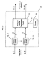
- optical crossbar switch 10 includes a plurality of optical splitters 15-1 through 15- N , array of optical conductors (array) 30 and control element 20.
- control element 20 is a stored-program control based-processor (e.g., a microprocessor) with associated memory (not shown) and will not be described further.
- N input optical channels e.g., optical fibers 9-1 to 9-N, each of which convey an optical signal (e.g., a OC192 WDM optical signal)
- splitters 15-1 to 15-N are applied to splitters 15-1 to 15-N, respectively.
- Each optical splitter splits an input optical signal into m duplicates (albeit at reduced power compared to the respective input optical signal).
- the m duplicates are also referred to herein as a group of m split signals.
- Array 30 comprises N x M optical conductors, where N > 0 , M > 0 , and M may equal N .
- Array 30 is also coupled to M optical fibers (or output optical channels) that provide M output optical signal paths.
- Control element 20 controls array 30, via control signaling 21, to switch each of the N input optical signals to one of the M output optical channels in accordance with a mapping table (described below) that maps signals appearing on each input optical channel to output optical channels.
- control element 20 turns on, and off, individual cells (i.e., optical conductors) of array 30 for switching at least one of the N input optical signals to at least one of the M output optical signal paths.
- FIG. 3 an illustrative top, front, and right side perspective view of an embodiment of array 30 is shown (not to scale). To simplify the description, the following exemplary definitions are made:
- array 30 comprises 16 optical conductors (i.e., (N)(M)) , of which optical conductor 1-1 is representative (described further below).
- Optical conductor 1-1 is the element, or cell, in the first row and first column of array 30.
- each row of array 30 is associated with a respective input optical channel and each column of array 30 is associated with a respective output optical channel.
- each input optical signal is spilt into 4 (i.e., M ) optical signals by a splitter as shown in FIG. 2.
- dashed box 50 of FIG. 3 an input optical signal is applied to the bottom of array 30, which provides output optical signals at its top.
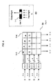
- FIG. 4 shows an alternative representation of array 30 of FIG. 3.
- array 30 is modeled as a two dimensional matrix of cells (e.g., cell 1-1 is in the upper left corner and cell 1-4 is in the upper right corner).
- I1, I2, I3, and I4 each of which are conveyed by input optical channels 9-1, 9-2, 9-3 and 9-4, respectively.
- Each input optical signal is applied to one row of array 30.
- each input optical signal e.g., I1
- Each of these optical signals is applied to a particular cell of array 30.
- input optical signal I1 is spit into four optical signals, each of which is applied to cells 1-1, 1-2, 1-3 and 1-4 as indicated by the four arrows emanating from the right side of splitter 15-1. This is also shown in dashed box 60 of FIG. 4 (described further below).
- the association of an input optical signal to each row of array 30 is illustrated again in FIG. 4 by row 2 of array 30.
- input optical signal I2 is split into four optical signals and is applied to cells 2-1, 2-2, 2-3, and 2-4.
- Each optical conductor (or cell) of array 30 is either in the ON state, which conducts (passes or transmits) optical signals (e.g., like a waveguide); or is in the OFF state, which significantly attenuates incident optical signals.
- each optical conductor in the ON state is transparent to light for coupling the signal from an input to an output or in the OFF state blocks the incident light.
- dashed box 60 of FIG. 4 which shows row 1 of array 30.
- cell 1-3 is ON and the remaining cells are OFF. Controlling of the ON or OFF state is provided by control element 20 (described below). It can be observed from FIG. 4 that each column of array 30 is associated with a respective output optical channel.
- columns 1, 2, 3 and 4 of array 30 are associated with output optical channels 11-1, 11-2, 11-3 and 11-4.
- control element 20 it is assumed that at most only one cell in a column is turned ON at a time by control element 20. (This is for illustrative purposes only, the inventive concept is not so limited.)
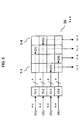
- a particular optical conductor in a column of array 30 is turned ON - the input optical signal conducted by that optical conductor is switched to a particular optical output channel in accordance with the principles of the invention. This is illustrated in FIG. 5.
- FIG. 5 As can be observed from FIG.
- control element 20 controls array 30 to switch an input optical signal to a particular one of the output optical channels. This is performed in accordance with a mapping table (or a cross-connect table) stored in memory (not shown) of control element 20.
- a mapping table or a cross-connect table
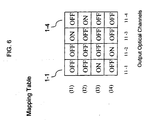
- An illustrative mapping table is shown in FIG. 6.
- the mapping table represents array 30. That is, the mapping table is also a 4x4 ( NxM ) array.
- NxM 4x4
- control element 20 turns cell 3-1 of array 30 ON, and turns OFF cells 1-1, 2-1, and 4-1 of column 1 thereby switching input optical signal I3 to output optical channel 11-1 (as also illustrated in FIG. 5).
- control element 20 is suitably programmed to carry out the above-described method using conventional programming techniques, which, as such, will not be described herein.
- the mapping table is simply a data structure of type "array,” and the ON and OFF states can be represented by, e.g., binary digits 1 and 0, respectively.
- initialization and updating of the mapping table (either in real-time, or, e.g., periodically) is not described herein. Such initialization and updates can be performed in any number of ways.
- optical crossbar switch 30 can be connected to a network control point (NCP) as known in the art for receiving switching information.)
- optical crossbar switch 300 comprises a plurality of optical splitters, here optical splitters 15 - 1 to 15 - k (which serve the input optical channels) and 15 - ( k +1) to 15 - N, which serve the add optical channels).
- Optical array 330 is an NxM array of optical conductors that enable a particular one of the optical signals conveyed on either the input optical channels or the add optical channels to be switched to one of the M output optical channels under the control of control element 320 (which includes a mapping table (not shown)).
- control element 320 which includes a mapping table (not shown)
- control element 320 controls optical array 330 to switch input optical signals, I1, I2, and I4 to output optical channels 11-1, 11-4 and 11-2, respectively.
- input optical signal I3 is dropped and optical signals A5 and A6 are added to output optical channels 11-5 and 11-6, respectively.
- the dropped optical signal 13 appears on output optical channel 11-7, which is designated as one of the drop channels. Therefore, and in accordance with the invention, add/drop capability is performed within the switch. That is, the add/drop feature is internal to the switch itself.
- an optical crossbar switch in accordance with the invention can also be modified to perform "multi-casting" within the switch itself.
- An illustrative mapping table is shown in FIG. 9 for multicasting input optical signal I2 to all output optical channels.
- the array of optical conductors comprises an array of modified liquid crystal pixels (LCPs) (herein referred to as, simply, LCPs).
- LCPs modified liquid crystal pixels
- Each LCP is illustratively constructed by adding a dichroic dye to the liquid crystal, where the liquid crystal has no polarizers.
- 4x4 array 30 is described.
- FIG. 10 a top, front, and right side perspective view of just row 1 of array 30 is shown (not to scale).
- row 1 comprises 4 optical conductors: cell 1-1, cell 1-2, cell 1-3 and cell 1-4.
- Representative cell 1-1 comprises a thin film transistor (TFT) 105 (i.e., a switching element), an LCP 110 that is switched to the OFF state by TFT 105, which is controlled by controller 20 (per, e.g., the mapping table of FIG. 6) via a column electrode and a row electrode (coupled to control signaling 21).
- TFT thin film transistor
- controller 20 per, e.g., the mapping table of FIG. 6
- the remaining LCPs, or cells, of row 1 are in the following states: cell 1-2 is OFF, cell 1-3 is ON and cell 1-4 is OFF.
- each LCP effectively acts as a shutter, which is either open or closed to the incident light.
- each LCP is passive, i.e., each LCP is not an active element in the sense of amplifying the incident optical signal.
- the inventive concept is not so limited.
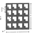
- FIG. 11 is an illustrative top plan view of array 30 (not to scale). It should be noted that a larger aperture ratio reduces loss and improves efficiency. Aperture Ratio can be increased by, e.g., reducing the area of the TFT and/or reducing the width of the row and column electrodes (also referred to as bus bars).
- FIG. 12 shows an illustrative PIOS structure.
- a splitter bulkhead 31 as known in the art, is used to split the input optical signals 9 for application to PIOS 32.
- an optical bulkhead 33 is used to provide the output optical signals 11 switched by PIOS 32.
- FIG. 12 shows an illustrative structure.
- the modified LCP is preferably an ultra black liquid crystal material as known in the art without a polarizer. Instead of a polarizer a dichroic dye is added to the liquid crystal. Other than the inventive concept, the use of dichroic dye in liquid crystals is known in the art. (Historically, dichroic dyes have been used in LCPs in place of polarizers.)
- dichroic dye in a liquid crystal is illustrated in FIG. 14.
- the dichroic dye blocks the transmission of the optical signal
- the dichroic dye enables transmission of the optical signal.
- the independently addressable, or selectable, LCPs either block, rotate or pass through an incident optical beam.
- Consideration in the design of LCPs is the ability to switch-in the OFF state without leakage, and provide minimum insertion loss in the ON state. Insertion loss between ranges of 1.9 to 3.0 dB are expected through an LCP shutter in the ON state with cross-talk of less than 40 dB. The insertion loss and can be further adjusted if needed using known optical design techniques.
- liquid crystal fluid selected is based on temperature range and cost desired, for example.
- Liquid crystal fluids ⁇ their temperature ranges and costs ⁇ are known in the art, and not described herein.
- a temperature range between -40°Celsius (C) and 85°C might be used.
- the amount of liquid crystal material and contrast e.g., amount of dichroic dye
- FIG. 15 shows an illustrative top elevational view (not to scale) of a portion of array 30.
- input optical channels 9-1, 9-2 and 9-2 are applied to the rows of the PIOS (note: the splitter is not shown for simplicity (e.g.; see FIGs. 12 and 13)), while columns of the PIOS are coupled to the optical bus for coupled to output optical channels 11-1, 11-2 and 11-3 via the optical bulkhead 33 (not shown in FIG. 15).
- FIG. 16 An illustrative structure for TFT 105 is shown in FIG. 16, which is a front elevational view (not to scale).
- FIG. 17 shows an illustrative structure for a passive matrix drive system for driving a PIOS.
- FIG. 18 shows an illustrative structure for an active matrix drive system.
- FIGs. 19 and 20 Portions of a suggested construction method for a PIOS switch is shown in FIGs. 19 and 20, which, since - other than the inventive concept - semiconductor construction is well-known in the art are not described herein.
- the inventive concept provides an optical conductor crossbar switch for cross-connecting high-speed optical signals such that all optical switching takes place in the light domain, through an array of optical conductors, or optical valves, under program control.
- This design results in the reduction, if not elimination, of the use of mechanical parts. For example, since the optical switching is performed without the mechanical adjustment of mirrors, improved performance should result with respect to cross-talk, propagation delay, and waveform distortion.
- the optical conductor crossbar switch provides an add/drop capability in real-time with delays in the micro second range.
- standardized link aggregation protocols may be applied as separate gigabit links.
- splitters capable of splitting out 1024 optical signals are known in the art. (Splitters are available from companies such as TECOS, Duesseldorf Germany; and Photonic Integration Research Inc., Ohio.) Such a splitter can be used to interface, e.g., to a 1024x1024 optical array in accordance with the principles of the invention.
Landscapes
- Engineering & Computer Science (AREA)
- Computer Networks & Wireless Communication (AREA)
- Use Of Switch Circuits For Exchanges And Methods Of Control Of Multiplex Exchanges (AREA)
- Liquid Crystal (AREA)
- Optical Communication System (AREA)
Abstract
An optical crossbar switch comprises an array of modified liquid crystal pixels
(LCPs) (herein referred to as, simply, LCPs). Each LCP is constructed by adding a
dichroic dye to the liquid crystal, where the liquid crystal has no polarizers. The array
comprises N x M LCPs, where N > 0, M > 0, and M may equal N. The array is coupled to
(a) N optical fibers (or input optical channels) for receiving N input optical signals, and (b)
M optical fibers (or output optical channels) that provide M output optical signal paths,
and (c) a control element. The latter turns on and off individual cells (i.e., LCPs) of the
array for switching at least one of the N input optical signals to at least one of the M
output optical signal paths.
Description
- This invention relates generally to optical switching and, more particularly, to optical crossbar switching.
- In the area of optical communications, there is a need to perform high-speed switching between a plurality of inputs and a plurality of outputs. One suggested approach is to use a two-dimensional (NxN) array of micro-mirrors as the basis for an intelligent crossbar switch that allows switching each one of N optical input channels to a particular one of N optical output channels. The movement of each micro-mirror is individually controlled, via attachment to a mechanical hinge, so that each micro-mirror is mechanically adjusted to be either reflective or non-reflective. This provides for arbitrary switching between a particular one of the N incoming optical channels and one of the N output optical channels. Merging micro-mirror technology with currently available submicron silicon CMOS (complementary-symmetry metal-oxide-semiconductor) fabrication technologies provides for optical switching at the chip level. This provides the ability to perform NxN switching with low signal attenuation in a very compact volume.
- Unfortunately, such mechanical assemblies may produce cross-talk, propagation delay and wavelength distortion. In addition, these mechanical assembly chip-based systems may be costly, temperature sensitive and require periodic recalibration.
- An optical switch comprising an array of optical conductors for switching at least one input optical signal to at least one of a plurality of output optical signal paths.
- In an embodiment of the invention, the array of optical conductors comprises an array of modified liquid crystal pixels (LCPs) (herein referred to as, simply, LCPs). Each LCP is illustratively constructed by adding a dichroic dye to the liquid crystal, where the liquid crystal has no polarizers. The array comprises N x M LCPs, where N > 0, M > 0, and M may equal N. The array is coupled to (a) N optical fibers (or input optical channels) for receiving N input optical signals, and (b) M optical fibers (or output optical channels) that provide M output optical signal paths, and (c) a control element. The latter turns on and off individual cells (i.e., LCPs) of the array for switching at least one of the N input optical signals to at least one of the M output optical signal paths.
-
- FIG. 1 shows an illustrative block diagram of an optical crossbar switch in accordance with the principles of the invention;
- FIG. 2 shows another illustrative block diagram of an optical crossbar switch in accordance with the principles of the invention;
- FIGs. 3 - 5 shows an illustrative diagram of an array of optical conductors in accordance with the principles of the invention;
- FIG. 6 shows an illustrative mapping table;
- FIG. 7 shows another illustrative embodiment of an optical crossbar switch in accordance with the principles of the invention;
- FIGs. 8 and 9 show other illustrative mapping tables;
- FIG. 10 shows an illustrative row of optical conductors in accordance with the principles of the invention;
- FIG. 11 shows an illustrative top plan view of an optical conductor array comprising liquid crystal pixels;
- FIGs. 12 - 18 show illustrative semiconductor structures; and
- FIGs. 19 - 20 show a portion of a construction method of a pixeled image optical switch.
-
- An illustrative embodiment of the invention is shown in FIG. 1. Other than the inventive concept, the elements shown in FIG. 1 are well-known and will not be described in detail. For example, input optical channels, such as optical fibers, are well-known in the art and are not described herein. In accordance with the inventive concept, an
optical crossbar switch 10 switches any one of N input optical signals (present on one of N input optical channels 9) to any one of M outputoptical channels 11. For the purposes of this example, it is assumed that each input optical signal conforms to, e.g., Optical Carrier (OC) 192, which is an optical signal format standard supporting transmission in the Gigabit per second (Gbps) range for use in a Synchronous Optical Network (SONET) (not shown), which may further include wavelength division multiplexed (WDM) optical signals. - Another illustration of
optical crossbar switch 10 is shown in FIG. 2.Optical crossbar switch 10 includes a plurality of optical splitters 15-1 through 15-N, array of optical conductors (array) 30 andcontrol element 20. Again, other than the inventive concept, the elements shown in FIG. 2 are well-known and will not be described in detail. For example an optical splitter is well-known in the art. Similarly,control element 20 is a stored-program control based-processor (e.g., a microprocessor) with associated memory (not shown) and will not be described further. (Also, it should be noted that although the optical splitters are shown as a part ofoptical crossbar switch 10, this is for illustration purposes only and, e.g., could be placed external tooptical crossbar switch 10.) - As shown in FIG. 2, N input optical channels (e.g., optical fibers) 9-1 to 9-N, each of which convey an optical signal (e.g., a OC192 WDM optical signal), are applied to splitters 15-1 to 15-N, respectively. Each optical splitter splits an input optical signal into m duplicates (albeit at reduced power compared to the respective input optical signal). The m duplicates are also referred to herein as a group of m split signals.
Array 30 comprises N x M optical conductors, where N > 0, M > 0, and M mayequal N. Array 30 is coupled to the N input optical channels, via the respective splitters. For this example, it is assumed that m =M . Array 30 is also coupled to M optical fibers (or output optical channels) that provide M output optical signal paths.Control element 20controls array 30, viacontrol signaling 21, to switch each of the N input optical signals to one of the M output optical channels in accordance with a mapping table (described below) that maps signals appearing on each input optical channel to output optical channels. In other words,control element 20 turns on, and off, individual cells (i.e., optical conductors) ofarray 30 for switching at least one of the N input optical signals to at least one of the M output optical signal paths. - Turning now to FIG. 3, an illustrative top, front, and right side perspective view of an embodiment of
array 30 is shown (not to scale). To simplify the description, the following exemplary definitions are made: - N represents the number of rows of
array 30; - M represents the number of columns of
array 30; and - N = 4, M = 4, i.e.,
array 30 comprises a 4x4 array of optical conductors fur switching any one of 4 input optical signals to 4 output optical channels. - As shown in FIG. 3,
array 30 comprises 16 optical conductors (i.e., (N)(M)), of which optical conductor 1-1 is representative (described further below). Optical conductor 1-1 is the element, or cell, in the first row and first column ofarray 30. As described further below, each row ofarray 30 is associated with a respective input optical channel and each column ofarray 30 is associated with a respective output optical channel. Sincearray 30 has 4 columns (i.e., M = 4), each input optical signal is spilt into 4 (i.e., M) optical signals by a splitter as shown in FIG. 2. As indicated by dashedbox 50 of FIG. 3, an input optical signal is applied to the bottom ofarray 30, which provides output optical signals at its top. In order to continue the description, attention should now be directed to FIG. 4, which shows an alternative representation ofarray 30 of FIG. 3. - In FIG. 4,
array 30 is modeled as a two dimensional matrix of cells (e.g., cell 1-1 is in the upper left corner and cell 1-4 is in the upper right corner). As can be seen on FIG. 4, there are four input optical signals I1, I2, I3, and I4, each of which are conveyed by input optical channels 9-1, 9-2, 9-3 and 9-4, respectively. Each input optical signal is applied to one row ofarray 30. In particular, each input optical signal (e.g., I1) is further duplicated by a corresponding splitter (e.g., 15-1) into M = 4 optical signals. Each of these optical signals is applied to a particular cell ofarray 30. For example, input optical signal I1 is spit into four optical signals, each of which is applied to cells 1-1, 1-2, 1-3 and 1-4 as indicated by the four arrows emanating from the right side of splitter 15-1. This is also shown in dashedbox 60 of FIG. 4 (described further below). The association of an input optical signal to each row ofarray 30 is illustrated again in FIG. 4 byrow 2 ofarray 30. As can be seen inrow 2 ofarray 30, input optical signal I2 is split into four optical signals and is applied to cells 2-1, 2-2, 2-3, and 2-4. - Each optical conductor (or cell) of
array 30 is either in the ON state, which conducts (passes or transmits) optical signals (e.g., like a waveguide); or is in the OFF state, which significantly attenuates incident optical signals. In other words, each optical conductor in the ON state is transparent to light for coupling the signal from an input to an output or in the OFF state blocks the incident light. This is illustrated in dashedbox 60 of FIG. 4, which showsrow 1 ofarray 30. In this example, cell 1-3 is ON and the remaining cells are OFF. Controlling of the ON or OFF state is provided by control element 20 (described below). It can be observed from FIG. 4 that each column ofarray 30 is associated with a respective output optical channel. In this example,columns array 30 are associated with output optical channels 11-1, 11-2, 11-3 and 11-4. For this example, it is assumed that at most only one cell in a column is turned ON at a time bycontrol element 20. (This is for illustrative purposes only, the inventive concept is not so limited.) As such, when a particular optical conductor in a column ofarray 30 is turned ON - the input optical signal conducted by that optical conductor is switched to a particular optical output channel in accordance with the principles of the invention. This is illustrated in FIG. 5. As can be observed from FIG. 5, the following optical conductors (cells) are turned ON: cells 3-1, 4-2, 1-3 and 2-4 ― thus switching (or cross-connecting) input optical signals I1, I2, I3 and I4 to output optical channels 11-3, 11-4, 11-1 and 11-2, respectively. - As noted above,
control element 20controls array 30 to switch an input optical signal to a particular one of the output optical channels. This is performed in accordance with a mapping table (or a cross-connect table) stored in memory (not shown) ofcontrol element 20. An illustrative mapping table is shown in FIG. 6. The mapping table representsarray 30. That is, the mapping table is also a 4x4 (NxM) array. As can be observed from FIG. 6, cells 3-1, 4-2, 1-3 and 2-4 of the mapping table are turned ON and the remaining cells are turned OFF Thus, the stored program controlled processor (not shown) ofcontrol element 20controls array 30 in accordance with the corresponding entries in the mapping table. For example,control element 20 turns cell 3-1 ofarray 30 ON, and turns OFF cells 1-1, 2-1, and 4-1 ofcolumn 1 thereby switching input optical signal I3 to output optical channel 11-1 (as also illustrated in FIG. 5). It is presumed thatcontrol element 20 is suitably programmed to carry out the above-described method using conventional programming techniques, which, as such, will not be described herein. (For example, the mapping table is simply a data structure of type "array," and the ON and OFF states can be represented by, e.g.,binary digits 1 and 0, respectively. Similarly, initialization and updating of the mapping table (either in real-time, or, e.g., periodically) is not described herein. Such initialization and updates can be performed in any number of ways. For example,optical crossbar switch 30 can be connected to a network control point (NCP) as known in the art for receiving switching information.) - Another embodiment of an optical crossbar switch is shown in FIG. 7. This embodiments is similar to the embodiment of FIG. 2 except that a portion of the input optical signals are "add" signals. Like FIG. 2,
optical crossbar switch 300 comprises a plurality of optical splitters, here optical splitters 15 - 1 to 15 - k (which serve the input optical channels) and 15 - (k+1) to 15 - N, which serve the add optical channels).Optical array 330 is an NxM array of optical conductors that enable a particular one of the optical signals conveyed on either the input optical channels or the add optical channels to be switched to one of the M output optical channels under the control of control element 320 (which includes a mapping table (not shown)). In addition, the embodiment of FIG. 7 provides the ability to simply "drop" optical signals as known in the art. As further illustration, assume that N = 6, of which 4 are input optical channels conveying input optical signals I1, I2, I3 and I4, respectively, and 2 are add optical channels conveying add optical signals A4 and A5, respectively. In addition, assume that there are M = 8 output optical channels. An illustrative mapping table for use bycontrol element 320 is shown in FIG. 8. As can be observed from FIG. 8,control element 320 controlsoptical array 330 to switch input optical signals, I1, I2, and I4 to output optical channels 11-1, 11-4 and 11-2, respectively. In addition, input optical signal I3 is dropped and optical signals A5 and A6 are added to output optical channels 11-5 and 11-6, respectively. The droppedoptical signal 13 appears on output optical channel 11-7, which is designated as one of the drop channels. Therefore, and in accordance with the invention, add/drop capability is performed within the switch. That is, the add/drop feature is internal to the switch itself. - Similar to the add/drop capability illustrated by the mapping table of FIG. 8, an optical crossbar switch in accordance with the invention can also be modified to perform "multi-casting" within the switch itself. An illustrative mapping table is shown in FIG. 9 for multicasting input optical signal I2 to all output optical channels.
- In an embodiment of the invention, the array of optical conductors comprises an array of modified liquid crystal pixels (LCPs) (herein referred to as, simply, LCPs). Each LCP is illustratively constructed by adding a dichroic dye to the liquid crystal, where the liquid crystal has no polarizers. As illustration,
4x4 array 30 is described. Turning to FIG. 10, a top, front, and right side perspective view of just row 1 ofarray 30 is shown (not to scale). As noted above (also see FIG. 3),row 1 comprises 4 optical conductors: cell 1-1, cell 1-2, cell 1-3 and cell 1-4. Representative cell 1-1 comprises a thin film transistor (TFT) 105 (i.e., a switching element), anLCP 110 that is switched to the OFF state byTFT 105, which is controlled by controller 20 (per, e.g., the mapping table of FIG. 6) via a column electrode and a row electrode (coupled to control signaling 21). The remaining LCPs, or cells, ofrow 1 are in the following states: cell 1-2 is OFF, cell 1-3 is ON and cell 1-4 is OFF. Thus, each LCP effectively acts as a shutter, which is either open or closed to the incident light. (It should be observed that each LCP is passive, i.e., each LCP is not an active element in the sense of amplifying the incident optical signal. However, the inventive concept is not so limited.) - With respect to an array of LCPs, the following exemplary definitions are made:
- Array Width =
- D;
- Array Height =
- C;
- Pixel Width =
- a;
- Pixel Height =
- b;
- Pixel Pitch =
- the measurement from the center of one pixel to the center of the next adjacent pixel;
- Pixel Aspect Ratio =
- the ratio between the height of a pixel and the width of the pixel - b/a;
- Pixel Area =
- (b)(a);
- Total Pixel Area =
- (N)(M)(b)(a), where N and M are the array dimensions;
- Total Array Area =
- (C)(D);
- Fill Factor =
- (Total Pixel Area/Total Array Area);
- TFT (thin film transistor) width =
- e;
- TFT height =
- f;
- TFT area =
- (e)(f);
- Pixel Opening =
- (Pixel Area - TFT area); and
- Aperture Ratio =
- Pixel Opening/Pixel Area.
- These definitions are illustrated with respect to
array 30 in FIG. 11, which is an illustrative top plan view of array 30 (not to scale). It should be noted that a larger aperture ratio reduces loss and improves efficiency. Aperture Ratio can be increased by, e.g., reducing the area of the TFT and/or reducing the width of the row and column electrodes (also referred to as bus bars). - As used herein, the term "Pixel Image Optical Switch (PIOS)" refers to
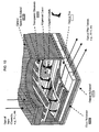
optical array 30 whenoptical array 30 comprises an array of LCPs. Illustrative semiconductor structures for use in a PIOS are shown in FIGs. 12, 13, 14, 15, 16 and 17. Other than the inventive concept, semiconductor fabrication is known in the art and is not described herein. FIG. 12 shows an illustrative PIOS structure. As can be observed from FIG. 12, asplitter bulkhead 31, as known in the art, is used to split the inputoptical signals 9 for application toPIOS 32. Similarly, anoptical bulkhead 33 is used to provide the outputoptical signals 11 switched byPIOS 32. A portion of a more detailed illustrative structure is shown in FIG. 13, which is a top, front, right side cut-away perspective view (not to scale). The modified LCP is preferably an ultra black liquid crystal material as known in the art without a polarizer. Instead of a polarizer a dichroic dye is added to the liquid crystal. Other than the inventive concept, the use of dichroic dye in liquid crystals is known in the art. (Historically, dichroic dyes have been used in LCPs in place of polarizers.) - The affect of dichroic dye in a liquid crystal is illustrated in FIG. 14. In the OFF state, the dichroic dye blocks the transmission of the optical signal, while in the ON state, the dichroic dye enables transmission of the optical signal. Thus, the independently addressable, or selectable, LCPs either block, rotate or pass through an incident optical beam. Consideration in the design of LCPs is the ability to switch-in the OFF state without leakage, and provide minimum insertion loss in the ON state. Insertion loss between ranges of 1.9 to 3.0 dB are expected through an LCP shutter in the ON state with cross-talk of less than 40 dB. The insertion loss and can be further adjusted if needed using known optical design techniques. The type of liquid crystal fluid selected is based on temperature range and cost desired, for example. (Liquid crystal fluids ― their temperature ranges and costs ― are known in the art, and not described herein.) As illustration, a temperature range between -40°Celsius (C) and 85°C might be used. The amount of liquid crystal material and contrast (e.g., amount of dichroic dye) depend upon the selected cell size, speed of liquid crystal fluid and other design constraints. It should be noted that since the above-described PIOS interfaces directly to single or multi-mode fiber (e.g., via the splitter and bulkhead) an optical translator is not required. For completeness, FIG. 15 shows an illustrative top elevational view (not to scale) of a portion of
array 30. It should be noted that input optical channels 9-1, 9-2 and 9-2 are applied to the rows of the PIOS (note: the splitter is not shown for simplicity (e.g.; see FIGs. 12 and 13)), while columns of the PIOS are coupled to the optical bus for coupled to output optical channels 11-1, 11-2 and 11-3 via the optical bulkhead 33 (not shown in FIG. 15). - An illustrative structure for
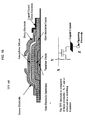
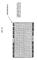
TFT 105 is shown in FIG. 16, which is a front elevational view (not to scale). FIG. 17 shows an illustrative structure for a passive matrix drive system for driving a PIOS. Alternatively, FIG. 18 shows an illustrative structure for an active matrix drive system. - Portions of a suggested construction method for a PIOS switch is shown in FIGs. 19 and 20, which, since - other than the inventive concept - semiconductor construction is well-known in the art are not described herein.
- As described above, the inventive concept provides an optical conductor crossbar switch for cross-connecting high-speed optical signals such that all optical switching takes place in the light domain, through an array of optical conductors, or optical valves, under program control. This design results in the reduction, if not elimination, of the use of mechanical parts. For example, since the optical switching is performed without the mechanical adjustment of mirrors, improved performance should result with respect to cross-talk, propagation delay, and waveform distortion. In addition, and as described above, the optical conductor crossbar switch provides an add/drop capability in real-time with delays in the micro second range. In addition, due to optical design of the switch, standardized link aggregation protocols may be applied as separate gigabit links.
- The foregoing merely illustrates the principles of the invention and it will thus be appreciated that those skilled in the art will be able to devise numerous alternative arrangements which, although not explicitly described herein, embody the principles of the invention and are within its scope. For example, although the illustrative embodiment described the use of N input optical channels and M output optical channels, the number of input optical channels can be less than N, and the number of output optical channels can be less than M. In addition, although described in the context of enabling only one optical conductor in a column at a time, multiple optical conductors could be enable at the same time in the same row ― care should be taken with respect to the signal level of the resulting combined signal. Further, although described in the context of a modified LCP, other equivalent optical conductors also fall within the scope of the invention as claimed below. For example, an LCP constructed with polarizers can also be used. In this case, care must be taken with respect to the amount of optical loss introduced by the polarizers. Similarly, although the inventive concept was illustrated in terms of a two dimensional 4x4 optical array, other dimensions and sizes may be possible. For example, splitters capable of splitting out 1024 optical signals are known in the art. (Splitters are available from companies such as TECOS, Duesseldorf Germany; and Photonic Integration Research Inc., Ohio.) Such a splitter can be used to interface, e.g., to a 1024x1024 optical array in accordance with the principles of the invention.
Claims (12)
- Apparatus for switching optical signals, the apparatus comprising:an array of optical elements, wherein each optical element is controllable to be either transparent to an optical signal or block an optical signal, and wherein the array is at least two-dimensional having dimensions of at least N x M, wherein N > 0, M > 0, and M may equal N; anda controller for controlling the array to switch at least one of n optical signals applied to the array to at least one of m output optical signal paths coupled to the array, where 1 < n ≤ N, and 1 ≤ m ≤ M.
- The apparatus of claim 1 wherein the controller controls the array to multicast at least one of the n optical signals to at least two of the m output optical signals.
- The apparatus of claim 1 wherein the controller controls the array in such a way to be able to add and drop optical signals.
- The apparatus of claim 1 further comprising at least one splitter for dividing at least one of the n optical signals into m split optical signals, which are applied to a row of the array.
- The apparatus of claim 1 wherein each optical element comprises a liquid crystal.
- The apparatus of claim 5 wherein each optical element further comprises a switching element for controlling an ON and OFF state of the liquid crystal.
- The apparatus of claim 5 wherein a dichroic dye is added to each liquid crystal.
- The apparatus of claim 5 wherein each liquid crystal further comprises a polarizer.
- The apparatus of claim 1 wherein the array of optical elements comprises an array of liquid crystals that are capable of being individually addressed for performing the switching.
- The apparatus of claim 9 wherein each optical element further comprises a switching element for controlling an ON and OFF state of an associated liquid crystal of the liquid crystal array.
- The apparatus of claim 9 wherein a dichroic dye is added to each liquid crystal.
- The apparatus of claim 9 wherein each liquid crystal further comprises a polarizer.
Applications Claiming Priority (2)
| Application Number | Priority Date | Filing Date | Title |
|---|---|---|---|
| US47863000A | 2000-01-06 | 2000-01-06 | |
| US478630 | 2000-01-06 |
Publications (1)
| Publication Number | Publication Date |
|---|---|
| EP1115257A1 true EP1115257A1 (en) | 2001-07-11 |
Family
ID=23900718
Family Applications (1)
| Application Number | Title | Priority Date | Filing Date |
|---|---|---|---|
| EP00306692A Withdrawn EP1115257A1 (en) | 2000-01-06 | 2000-08-07 | An optical crossbar switch |
Country Status (3)
| Country | Link |
|---|---|
| EP (1) | EP1115257A1 (en) |
| JP (1) | JP2001228490A (en) |
| CA (1) | CA2327401A1 (en) |
Cited By (1)
| Publication number | Priority date | Publication date | Assignee | Title |
|---|---|---|---|---|
| CN105549232A (en) * | 2015-12-08 | 2016-05-04 | 华中科技大学 | Bimodule integrated electronic controlled liquid crystal optical switch array |
Citations (2)
| Publication number | Priority date | Publication date | Assignee | Title |
|---|---|---|---|---|
| US5227905A (en) * | 1980-01-08 | 1993-07-13 | Clark Noel A | Surface stabilized ferroelectric liquid crystal devices |
| US5255332A (en) * | 1992-07-16 | 1993-10-19 | Sdl, Inc. | NxN Optical crossbar switch matrix |
-
2000
- 2000-08-07 EP EP00306692A patent/EP1115257A1/en not_active Withdrawn
- 2000-11-27 CA CA002327401A patent/CA2327401A1/en not_active Abandoned
- 2000-12-22 JP JP2000389862A patent/JP2001228490A/en active Pending
Patent Citations (2)
| Publication number | Priority date | Publication date | Assignee | Title |
|---|---|---|---|---|
| US5227905A (en) * | 1980-01-08 | 1993-07-13 | Clark Noel A | Surface stabilized ferroelectric liquid crystal devices |
| US5255332A (en) * | 1992-07-16 | 1993-10-19 | Sdl, Inc. | NxN Optical crossbar switch matrix |
Non-Patent Citations (3)
| Title |
|---|
| HIMENO A ET AL: "4 X 4 OPTICAL-GATE MATRIX SWITCH", JOURNAL OF LIGHTWAVE TECHNOLOGY,IEEE. NEW YORK,US, vol. 3, no. 2, 1 April 1985 (1985-04-01), pages 230 - 235, XP000567913, ISSN: 0733-8724 * |
| MASAYASU YAMAGUCHI ET AL: "RECENT FREE-SPACE PHOTONIC SWITCHES", IEICE TRANSACTIONS ON COMMUNICATIONS,INSTITUTE OF ELECTRONICS INFORMATION AND COMM. ENG. TOKYO,JP, vol. E77-B, no. 2, 1 February 1994 (1994-02-01), pages 128 - 138, XP000447103, ISSN: 0916-8516 * |
| PATEL J S ET AL: "LIQUID CRYSTAL AND GRATING-BASED MULTIPLE-WAVELENGTH CROSS-CONNECT SWITCH", IEEE PHOTONICS TECHNOLOGY LETTERS,IEEE INC. NEW YORK,US, vol. 7, no. 5, 1 May 1995 (1995-05-01), pages 514 - 516, XP000506797, ISSN: 1041-1135 * |
Cited By (2)
| Publication number | Priority date | Publication date | Assignee | Title |
|---|---|---|---|---|
| CN105549232A (en) * | 2015-12-08 | 2016-05-04 | 华中科技大学 | Bimodule integrated electronic controlled liquid crystal optical switch array |
| CN105549232B (en) * | 2015-12-08 | 2019-01-04 | 华中科技大学 | A kind of double-mode integrated electrically-controlled liquid crystal array of photoswitch |
Also Published As
| Publication number | Publication date |
|---|---|
| JP2001228490A (en) | 2001-08-24 |
| CA2327401A1 (en) | 2001-07-06 |
Similar Documents
| Publication | Publication Date | Title |
|---|---|---|
| Yoo | Prospects and challenges of photonic switching in data centers and computing systems | |
| US6657770B2 (en) | Programmable optical multiplexer/demultiplexer | |
| JP3842511B2 (en) | Optical spatial switch using multiport coupler | |
| US8233794B2 (en) | Hitless MxN wavelength selective switch | |
| Shibata et al. | Silica-based waveguide-type 16 x 16 optical switch module incorporating driving circuits | |
| US6275312B1 (en) | Optical routing switch | |
| CA2353744C (en) | Nxn crossconnect switch using wavelength routers and space switches | |
| US5751868A (en) | Asymetrically dilated optical cross connect switches | |
| US6819821B2 (en) | Optical switch with a geometry based on perpendicularly-oriented planar lightwave circuit switches | |
| Doerr et al. | Eight-wavelength add-drop filter with true reconfigurability | |
| Watanabe et al. | Silica-based PLC 1/spl times/128 thermo-optic switch | |
| US7321704B2 (en) | Wavelength cross connect with per port performance characteristics | |
| US6839472B1 (en) | Solid state optical interconnect system | |
| EP1288704A1 (en) | Optical crossbar switch based on switchable diffraction gratings | |
| EP4460034A1 (en) | Extendable optical circuit switch architecture | |
| CA2327401A1 (en) | An optical crossbar switch | |
| EP1371260B1 (en) | Polarization independent non-bloking all-optical switching device | |
| Doerr et al. | Silica-waveguide 1× 9 wavelength-selective cross connect | |
| Kwon et al. | Large-scale silicon photonic switches | |
| Yamaguchi et al. | Recent free-space photonic switches | |
| Fracasso et al. | Performance assessment of a liquid crystal multichannel photonic space-switch | |
| WO2026091430A1 (en) | Optical device and optical switching device | |
| Yuan et al. | Low interchannel crosstalk high speed fiber optic N/spl times/N crossconnect switch using polarization optics and ferroelectric liquid crystals | |
| Chen et al. | Design and applications of large-scale integrated planar lightwave circuits for WDM systems | |
| O'Donnell et al. | A 1* 32 polarisation independent switch for analogue systems |
Legal Events
| Date | Code | Title | Description |
|---|---|---|---|
| PUAI | Public reference made under article 153(3) epc to a published international application that has entered the european phase |
Free format text: ORIGINAL CODE: 0009012 |
|
| 17P | Request for examination filed |
Effective date: 20000817 |
|
| AK | Designated contracting states |
Kind code of ref document: A1 Designated state(s): DE FR GB |
|
| AX | Request for extension of the european patent |
Free format text: AL;LT;LV;MK;RO;SI |
|
| AKX | Designation fees paid |
Free format text: DE FR GB |
|
| STAA | Information on the status of an ep patent application or granted ep patent |
Free format text: STATUS: THE APPLICATION IS DEEMED TO BE WITHDRAWN |
|
| 18D | Application deemed to be withdrawn |
Effective date: 20040302 |