EP1115222A2 - CDMA encoder-decoder, CDMA communication system, WDM-CDMA communication system - Google Patents
CDMA encoder-decoder, CDMA communication system, WDM-CDMA communication system Download PDFInfo
- Publication number
- EP1115222A2 EP1115222A2 EP00311772A EP00311772A EP1115222A2 EP 1115222 A2 EP1115222 A2 EP 1115222A2 EP 00311772 A EP00311772 A EP 00311772A EP 00311772 A EP00311772 A EP 00311772A EP 1115222 A2 EP1115222 A2 EP 1115222A2
- Authority
- EP
- European Patent Office
- Prior art keywords
- input
- cdma
- optical
- delay lines
- parts
- Prior art date
- Legal status (The legal status is an assumption and is not a legal conclusion. Google has not performed a legal analysis and makes no representation as to the accuracy of the status listed.)
- Granted
Links
Images










Classifications
-
- G—PHYSICS
- G02—OPTICS
- G02B—OPTICAL ELEMENTS, SYSTEMS OR APPARATUS
- G02B6/00—Light guides; Structural details of arrangements comprising light guides and other optical elements, e.g. couplings
- G02B6/10—Light guides; Structural details of arrangements comprising light guides and other optical elements, e.g. couplings of the optical waveguide type
- G02B6/12—Light guides; Structural details of arrangements comprising light guides and other optical elements, e.g. couplings of the optical waveguide type of the integrated circuit kind
- G02B6/12007—Light guides; Structural details of arrangements comprising light guides and other optical elements, e.g. couplings of the optical waveguide type of the integrated circuit kind forming wavelength selective elements, e.g. multiplexer, demultiplexer
- G02B6/12009—Light guides; Structural details of arrangements comprising light guides and other optical elements, e.g. couplings of the optical waveguide type of the integrated circuit kind forming wavelength selective elements, e.g. multiplexer, demultiplexer comprising arrayed waveguide grating [AWG] devices, i.e. with a phased array of waveguides
- G02B6/12019—Light guides; Structural details of arrangements comprising light guides and other optical elements, e.g. couplings of the optical waveguide type of the integrated circuit kind forming wavelength selective elements, e.g. multiplexer, demultiplexer comprising arrayed waveguide grating [AWG] devices, i.e. with a phased array of waveguides characterised by the optical interconnection to or from the AWG devices, e.g. integration or coupling with lasers or photodiodes
- G02B6/12021—Comprising cascaded AWG devices; AWG multipass configuration; Plural AWG devices integrated on a single chip
-
- G—PHYSICS
- G02—OPTICS
- G02B—OPTICAL ELEMENTS, SYSTEMS OR APPARATUS
- G02B6/00—Light guides; Structural details of arrangements comprising light guides and other optical elements, e.g. couplings
- G02B6/24—Coupling light guides
- G02B6/26—Optical coupling means
- G02B6/28—Optical coupling means having data bus means, i.e. plural waveguides interconnected and providing an inherently bidirectional system by mixing and splitting signals
- G02B6/2804—Optical coupling means having data bus means, i.e. plural waveguides interconnected and providing an inherently bidirectional system by mixing and splitting signals forming multipart couplers without wavelength selective elements, e.g. "T" couplers, star couplers
- G02B6/2861—Optical coupling means having data bus means, i.e. plural waveguides interconnected and providing an inherently bidirectional system by mixing and splitting signals forming multipart couplers without wavelength selective elements, e.g. "T" couplers, star couplers using fibre optic delay lines and optical elements associated with them, e.g. for use in signal processing, e.g. filtering
-
- H—ELECTRICITY
- H04—ELECTRIC COMMUNICATION TECHNIQUE
- H04J—MULTIPLEX COMMUNICATION
- H04J14/00—Optical multiplex systems
- H04J14/005—Optical Code Multiplex
-
- H—ELECTRICITY
- H04—ELECTRIC COMMUNICATION TECHNIQUE
- H04J—MULTIPLEX COMMUNICATION
- H04J14/00—Optical multiplex systems
- H04J14/02—Wavelength-division multiplex systems
- H04J14/03—WDM arrangements
- H04J14/0305—WDM arrangements in end terminals
Definitions
- the present invention relates to an encoder-decoder, and a CDMA (Code Division Multiple Access) communication system, especially, relates to a CDMA encoder-decoder and a CDMA communication system in an optical area wherein encoding and decoding of a signal can be carried out.
- CDMA Code Division Multiple Access
- this invention relates to a WDM (Wavelength Division Multiplexing)-CDMA communication system in an optical area wherein a CDMA technique is applied to a WDM communication.
- WDM Widelength Division Multiplexing
- optical CDMA Code Division Multiple Access
- this system can be applicable to an optical LAN and an optical switching system.
- J natural number
- Each lattice-form optical circuit positioned at the left and right side of the star coupler corresponds to an encoder and a decoder, respectively.
- phase information produced at refractive index control parts (phase shifters) 5a and 5b in the waveguide of the lattice-form optical circuit 2b are phase information produced at refractive index control parts (phase shifters) 5a and 5b in the waveguide of the lattice-form optical circuit 2b.
- phase shifters phase shifters
- phase shifters 5c and 5d in the lattice-form optical circuit 2e satisfy the decoding conditions in contrast to phase shifters 5a and 5b, the optical power is concentrated in the center of each pulse to be decoded. However, when the settings do not satisfy the decoding conditions, an inputted encoded pulse is further spread in the time region and is not decoded.
- ⁇ a, ⁇ b, ⁇ c, and ⁇ d are phase shift values of the phase shifters 5a, 5b, 5c, and 5d, respectively.
- the conventional method described above has a problem that side lobe components are produced around the decoded optical pulse, and the S/N ratio (Signal to Noise ratio) at the receiver is deteriorated even when the decoding condition is satisfied.
- an encoded pattern can be decoded easily, thus causing a problem on the secrecy of communication that is one of the merits in the CDMA.
- An object of the present invention is to provide a CDMA encoder-decoder and a CDMA communication system that can reduce the output levels of an unnecessary side lobe component of an decoded optical signal pulse and a non-decoded optical signal pulse by increasing the number of encoding patterns, that is; that can improve both an auto-correction and cross-correlation characteristics, and the secrecy of communication.
- Another object of the invention is to provide a WDM-CDMA communication system that can decrease a wavelength channel interval in a WDM communication to improve the efficiency of frequency utilization by applying a CDMA encoding-decoding technique to the WDM communication.
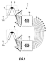
- Fig. 1 is a block diagram showing the configuration of an optical CDMA encoder-decoder according to a first embodiment of the present invention.
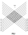
- Fig. 2 is an illustrative diagram showing a configuration example of matrix optical switches in Fig. 1.
- Fig. 3 is an illustrative diagram showing another configuration example of the matrix optical switches in Fig. 1.
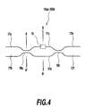
- Fig. 4 is an illustrative diagram showing the configuration example of 2 ⁇ 2 optical switches in Figs. 2 and 3.
- Figs. 5A and 5B are cross-section showing the configuration of waveguides in Fig. 4.
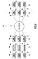
- Fig. 6 is a block diagram showing the configuration of an optical CDMA communication system according to a second embodiment of the present invention.
- Figs. 7A to 7E are illustrative diagram showing the input and output optical pulse train when the optical CDMA communication system shown in Fig. 6 is used.
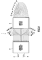
- Fig. 8 is an illustrative diagram showing the configuration of an optical CDMA encoder-decoder according to a third embodiment of the present invention.
- Fig. 9 is a diagram illustrating the configuration of an optical CDMA encoder-decoder according to a fourth embodiment of the present invention.
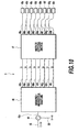
- Fig. 10 is a block diagram showing the configuration of an optical CDMA encoder-decoder according to a fifth embodiment of the present invention.
- Fig. 11 is an illustrative diagram showing the configuration example of a means for reflecting light shown in Fig. 10.
- Fig. 12 is a block diagram showing the configuration of an optical CDMA encoder-decoder according to a sixth embodiment of the present invention.
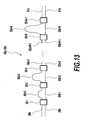
- Fig. 13 is a block diagram showing the configuration example of variable delay lines shown in Fig. 12.
- Fig. 14 is a block diagram showing the configuration example of the variable delay lines shown in Fig. 12.
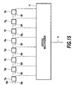
- Fig. 15 is a block diagram showing the configuration example of the variable delay lines shown in Fig. 12.
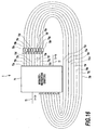
- Fig. 16 is a block diagram showing the configuration of an optical CDMA encoder-decoder according to a seventh embodiment of the present invention.
- Fig. 17 is a block diagram showing the configuration of an optical CDMA encoder-decoder according to an eighth embodiment of the present invention.
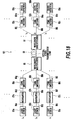
- Fig. 18 is a block diagram showing the configuration of an optical WDM-CDMA communication system according to a ninth embodiment of the present invention.
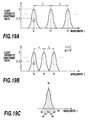
- Figs. 19A to 19C are illustrative diagrams showing the wavelength assignment in the optical WDM system and the WDM-CDMA communication system shown in Fig. 18.
- Fig. 20 is a block diagram showing a conventional optical CDMA encoder-decoder and optical CDMA communication system.
- Figs. 21A to 21D are illustrative diagrams showing the input and output optical pulse train when the optical CDMA encoder-decoder and the optical CDMA communication system shown in Fig. 20 is used.
- an optical CDMA encoder-decoder is constructed by connecting a first arrayed-waveguide grating, a first matrix optical switch, delay lines, a second matrix optical switch, and a second arrayed-waveguide grating in this order.
- Fig. 1 shows the configuration example of the optical CDMA encoder-decoder according to the present invention.
- An encoder and a decoder can be formed on separate substrates using the configuration shown in Fig. 1.
- the optical CDMA encoder-decoder 1 comprises an input part 6, slab waveguides 7a and 7b, arrayed-waveguides 8, arrayed-waveguide gratings 9a and 9b comprised of these slab waveguides and arrayed-waveguides, waveguides 10a-10p, matrix optical switches 11a and 11b, delay lines 12a-12h, and an output part 13.
- the arrayed-waveguide gratings 9a and 9b have functions of a wavelength demultiplexer and multiplexer, respectively.
- the optical path lengths are set so that the lengths are equal each other except the delay lines 12a-12h.
- a variety of light sources having a wide spectrum bandwidth can be used, that are inserted into the input part 6.
- a light emission diode (LED), a super luminescent diode (SLD), an amplified spontaneous emission (ASE) light source constructed by an optical fiber amplifier or a semiconductor laser amplifier, a supercontinuum (SC) light source, and a short pulse laser such as a semiconductor or an optical fiber mode-locked laser may be used.
- Light having a wide bandwidth emitted from these light sources is modulated with data by an optical intensity modulator and then the light is inserted into the input part 6.
- Fig. 2 shows an example of the matrix optical switches 11a and 11b constructed using an 8-input and 8-output (8 ⁇ 8) completely non-blocking configuration, assuming that eight frequency components are used.
- Designated 14a-14h, 15aa-15hh, and 16a-16h are the input parts, 2 ⁇ 2 optical switches, and the output parts, respectively.
- Fig. 3 shows another example of the matrix optical switches 11a and 11b constructed using an 8 ⁇ 8 completely non-blocking configuration.
- the configuration shown in Fig. 2 may cause loss fluctuation since the number of 2 ⁇ 2 optical switches 15 for connecting route differs depending on the selection of input and output ports.
- the light passes the optical switches 15 eight times if the connection route is selected as 14a ⁇ 15ah ⁇ 15bh ⁇ 15ch ⁇ 15dh ⁇ 15eh ⁇ 15fh ⁇ 15gh ⁇ 15hh ⁇ 16h.
- the light passes the optical switches 15 fifteen times if the connection route is selected as 14a ⁇ 15ah ⁇ 15ag ⁇ 15af ⁇ 15ae ⁇ 15ad ⁇ 15ac ⁇ 15ab ⁇ 15aa ⁇ 15ba ⁇ 15ca ⁇ 15da ⁇ 15ea ⁇ 15fa ⁇ 15ga ⁇ 15ha ⁇ 16h.
- the number of optical switches 15 differs depending on selected connection route.
- the configuration of Fig. 3 has an advantage of providing an equal loss in all selected connection routes between the input and output ports.
- Fig. 4 shows the configuration example of the 2 ⁇ 2 optical switches 15aa-15hh.
- This switch comprises waveguides 17a-17f, directional couplers 18a and 18b, and a refractive index control part 19 of a waveguide.
- Figs. 5A and B describe the cross-sections A-A' and B-B' in Fig. 4, respectively, viewed from the waveguides 17a and 17b in the direction of 17e and 17f.
- the optical CDMA encoder-decoder 1 in this example and the other examples described later is composed of a silica glass waveguide.
- SiO 2 under cladding layers 21a and 21b are deposited on Si substrates 20a and 20b by using the flame hydrolysis deposition.
- the core layer comprised of GeO 2 -doped SiO 2 glass is deposited and the two layers are consolidated using an electric furnace.
- the core layer is etched and cores 22a-22d are formed using an predetermined waveguide pattern.
- SiO 2 over cladding layers 23a and 23b are deposited and are consolidated using an electric furnace again.
- a thin-film heater 24 [used for the control of the refractive index (phase) of the waveguide based on the thermo-optic effect] and metal interconnection are evaporated on the predetermined over cladding layer.
- a symmetrical Mach-Zehnder interferometer is formed when the lengths of the directional couplers 18a and 18b, where two waveguides are arranged close to each other by several ⁇ m, are adjusted so as to provide a coupling coefficient of 0.5 and the lengths of the waveguides 17c and 17d are made equal.
- the other configuration examples of the directional coupler may be a single symmetrical Mach-Zehnder interferometer, cascaded symmetrical Mach-Zehnder interferometers in series, a multi-mode interference coupler (MMI), etc.
- MMI multi-mode interference coupler
- each spectrum component demultiplexed by the arrayed-waveguide grating is encoded in the time region by adding a delay time difference depending on the wavelength, which is based on the combination of the matrix optical switch and delay lines having different optical lengths. It is possible to set the combination of delay time and wavelengths arbitrarily.
- FIG. 6 A second embodiment of the present invention is explained by referring to Figs. 6 and 7. Explanation of the same components and numerals as those described in Fig. 1 is omitted.
- an optical CDMA communication system 100 is constructed by arbitrarily combining optical CDMA encoders and decoders that have been described above or will be referred later, and connecting an optical multiplexer and demultiplexer, and an optical transmission line between these encoders and decoders.
- the second embodiment is explained below by referring to specific examples.
- Fig. 6 shows the configuration example of the optical CDMA communication system 100 according to the present invention.
- This system is the optical CDMA communication system that is constructed by arbitrarily combining the optical CDMA encoders and decoders in Fig. 1 and in other examples described later.
- Reference numerals 25a-25c are light sources with wide spectrum bandwidth.
- Reference numerals 26a-26o are waveguides.
- Reference numerals 27a-27c are optical intensity modulators.
- Reference numerals 28a-28c are optical CDMA encoders.
- a reference numeral 29 is a star coupler.
- Reference numerals 30a-30c are optical CDMA decoders.
- Reference numerals 93a-93c are photo detectors.
- Reference numerals 26g-261 include optical transmission lines normally comprised of optical fibers.
- optical CDMA encoders and decoders 1 The operation of the optical CDMA encoders and decoders 1, and the optical CDMA communication system 100 having these encoders and decoders are explained below.
- the light sources with wide spectrum bandwidth 25a-25c have the same center wavelengths and spectrum characteristics.
- the light emitted from one light source with wide spectrum bandwidth may be divided into three to provide three light sources.
- optical intensity modulators 27a-27c are encoded by the optical CDMA encoders using different codes. Coding is carried out when assigning the wavelength components ⁇ 1 - ⁇ 8 demultiplexed by the arrayed-waveguide grating 9a in Fig. 1 to different delay lines by using the matrix optical switch 11a.
- the optical CDMA encoder 28a at the transmitter has relation between wavelengths and delay lines of ( ⁇ 1 , ⁇ 2 , ⁇ 3 , ⁇ 4 , ⁇ 5 , ⁇ 6 , ⁇ 7 , ⁇ 8 ) ⁇ (12d, 12f, 12c,12g, 12h, 12b, 12a, 12e) is given, and the optical CDMA encoder 28b has relation between wavelengths and delay lines of ( ⁇ 1 , ⁇ 2 , ⁇ 3 , ⁇ 4 , ⁇ 5 , ⁇ 6 , ⁇ 7 , ⁇ 8 ) ⁇ (12h, 12d, 12e, 12c, 12b, 12g, 12a, 12f).
- wavelength components ⁇ 1 - ⁇ 8 are inserted into the predetermined waveguides 10i-10p through the matrix switch 11b and are multiplexed by the arrayed-waveguide grating 9b, and further are sent to the star coupler 29 through an output part 13.
- the optical CDMA decoder 30c at the receiver carries out a decoding process that matches with the coding given by the optical CDMA encoder 28a, namely, ( ⁇ 1 , ⁇ 2 , ⁇ 3 , ⁇ 4 , ⁇ 5 , ⁇ 6 , ⁇ 7 , ⁇ 8 ) ⁇ (12e, 12c, 12f, 12b, 12a, 12g, 12h, 12d), so as to compensate for the delay time dependence on each wavelength given at 28a.
- Fig. 7A shows the optical pulses that have passed the optical intensity modulators 27a and 27b
- Figs. 7B and 7C show those that have passed the optical CDMA encoders 28a and 28b
- Figs. 7D and 7E show those that have passed the optical CDMA decoder 30c.
- the behavior of single pulse in an optical pulse train is demonstrated.
- Figs. 7A to 7E indicate that the optical pulses sent from 28a are decoded, but optical pluses from 28b are further spread at 30c in Fig. 6. This is because that each pulse spread caused by the delay time difference dependence on wavelength is compensated for by code matching, but the delay time difference is further expanded by the code non-matching.
- the decoded optical pulses are inserted into the photo detectors 93a-93c for data receiving.
- an optical CDMA system can be obtained where the wavelength components of an optical signal arbitrarily change with respect to time. Then it becomes possible to increase the number of coding patterns and then to improve the performance in the optical CDMA communication system.
- an optical CDMA encoder-decoder is constructed by connecting an arrayed-waveguide grating, a first matrix optical switch, delay lines, and a second matrix optical switch in this order, where the output parts of the second matrix optical switch and either the input or output parts of the arrayed-waveguide grating are connected.
- Fig. 8 shows the configuration example of the optical CDMA encoder-decoder 1.
- the CDMA encoder and the CDMA decoder are formed on separate substrates using the configuration shown in Fig. 8.
- the optical CDMA encoder-decoder 1 comprises an input part 31, arrayed-waveguide grating 32, waveguides 33a-33p, matrix optical switches 34a and 34b, delay lines 35a-35h, and an output part 36.
- the waveguides 33i-33p are connected to the unused input ports of the arrayed-waveguide grating 32, and one of the unused output ports in 32 is used as the output.
- the optical path lengths are made equal except the delay lines 35a-35h.
- the number of arrayed-waveguide gratings can be reduced to one in the configuration of Fig. 8, because the lights at the waveguides 33i-33p are concentrated to the output part 36 by utilizing the wavelength characteristics of the arrayed-waveguide grating.
- the operation as an optical CDMA encoder-decoder is the same as that of the second embodiment described above.
- the operation is the same when the waveguides 33i-33p are connected to the unused output ports of the arrayed-waveguide grating 32, and one of the unused input ports in 32 is used as the output part.
- the operation is the same when the waveguides 33i-33p are connected to the used input ports (output ports) of the arrayed-waveguide grating 32 through directional couplers, and one of the used output ports (input ports) in 32 is used as the output through a directional coupler, although the loss is increased.
- an optical CDMA encoder-decoder is constructed by connecting an arrayed-waveguide grating, a matrix optical switch, and delay lines in this order, where the unused end of each delay line is connected to either the input or output ports of the matrix optical switch, and the unused side ports of the matrix optical switch in this connection is connected to either the input or output ports of the arrayed-waveguide grating.
- Fig. 9 shows the configuration example of the optical CDMA encoder-decoder 1.
- the CDMA encoder and the CDMA decoder are formed on separate substrates using the configuration shown in Fig. 9.
- the optical CDMA encoder-decoder 1 comprises an input part 37, an arrayed-waveguide grating 38, waveguides 39a-39p, a matrix optical switch 40, delay lines 41a-41h, and an output part 42.
- Both ends of the delay lines 41a-41h are connected to the output ports of the matrix optical switch 40.
- Unused input ports of the matrix optical switch 40 are connected to unused output ports of the arrayed-waveguide grating 38 using the waveguides 39i-39p, and one of the unused input ports in 38 is used as the output part.
- the optical path lengths are made equal except the delay lines 41a-41h.
- the number of matrix optical switches and arrayed-waveguide gratings can be reduced to one in the configuration of Fig. 9, because the unused ports of the matrix optical switch are effectively utilized and the lights at the waveguides 39i-39p are concentrated to the output part 42 using the wavelength characteristics of the arrayed-waveguide grating.
- the operation as an optical CDMA encoder-decoder is the same as that of the second embodiment described above.
- the operation is the same when the unused ends of the delay lines 41a-41h are connected to the input ports of the matrix optical switch 40, the unused output ports of 40 are connected to the unused output ports (input ports) of the arrayed-waveguide grating 38, and one of the unused input ports (output ports) in 38 is used as the output part.
- an optical CDMA encoder-decoder 1 is constructed by connecting an arrayed-waveguide grating, a matrix optical switch, delay lines, and optical reflectors in this order.
- Fig. 10 shows the configuration example of the optical CDMA encoder-decoder 1.
- the CDMA encoder and the CDMA decoder are formed on separate substrates using the configuration shown in Fig. 10.
- the optical CDMA encoder-decoder 1 comprises an input part 43, a circulator 44, waveguides 45a-45i, an arrayed-waveguide grating 46, a matrix optical switch 47, delay lines 48a-48h, optical reflectors 49a-49h, and an output part 50.
- the other configuration example of the optical reflector described in Fig. 11 can be used in Fig. 10.
- a loop-form waveguide can be used as this optical reflector.
- Fig. 11 shows the configuration example of the optical reflectors 49a-49h.
- These optical reflectors 49a-49h comprise waveguides 51a-51c (51a, 51b: input or output part) and a directional coupler 52.
- the coupling coefficient of the directional coupler 52 is set at 0.5, the light inserted into 51a is divided into two lights with an intensity ratio of 1:1 that run in the clockwise (reflected at the directional coupler 52) and counter-clockwise (passing through the directional coupler 52) directions.
- phase changes of the lights that are reflected by and pass through the directional coupler 52 are zero and ⁇ /2, respectively, and the phase changes caused by the waveguide 51c are the same regardless of circulating directions. As a result, all the lights are outputted at the waveguide 51a.
- the optical path lengths are made equal except the delay lines 48a-48h.
- the light is reflected by the optical reflector 49 and the reflected light passes the same route as that of the incident light toward the opposite direction, and finally the light is outputted at the waveguide 45a.
- a 2 ⁇ 2 directional coupler can be used as output part of light. But, in this case, the part 50 is used as output using a circulator 44 to decrease the loss.
- the optical CDMA encoder-decoder is constructed by connecting a first arrayed-waveguide grating, variable delay lines, and a second arrayed-waveguide grating in this order.
- Fig. 12 shows the configuration example of the optical CDMA encoder-decoder 1.
- the CDMA encoder and the CDMA decoder are formed on separate substrates using the configuration shown in Fig. 12.
- the optical CDMA encoder-decoder 1 comprises an input part 53, arrayed-waveguide gratings 54a, 54b, waveguides 55a-55p, variable delay lines 56a-56h, and an output part 57.
- variable delay lines described in Fig. 13 can be used in Fig. 12.
- Cascaded asymmetrical Mach-Zehnder interferometers in series can be used as the variable delay lines.
- Fig. 13 shows the configuration example of the variable delay lines 56a-56h.
- variable delay lines 56a-56h are constructed using input waveguides 58a and 58b, 2 ⁇ 2 optical switches 59-1 to 59-N+1(N: natural number), pairs of asymmetrical arms 60a-1 to 60a-N and 60b-1 to 60b-N, and output waveguides 61a and 61b.
- Either 58a or 58b is used as the input, and either 61a or 61b is used as the output.
- Various optical lengths can be set when changing the switching state of the 2 ⁇ 2 optical switch 59, and then the variable delay lines can be realized.
- variable delay lines are arranged so that the optical path length difference becomes larger from the left to right in Fig. 13, however, the configuration is not restricted to this.
- interferometers can be arranged in any order, that is; the function of variable delay lines is independent of the order of the interferometers.
- optical path length difference in each asymmetrical Mach-Zehnder interferometer is made equal or interferometers having various optical path length differences are arbitrarily cascaded.
- the number of interferometers can be reduced to three when interferometers, of which optical path length differences are increased by a multiple of two, are cascaded.
- variable delay lines in which interferometers, of which optical path length differences are increased by a multiple of an arbitrary real number, are cascaded.
- interferometers of which optical path length differences are increased by a multiple of an arbitrary real number
- variable delay lines described in Fig. 14 can be used in Fig. 12.
- Fig. 14 shows other example of the configuration of the variable delay lines 56a-56h in Fig. 12.
- variable delay lines 56a-56h is constructed using an input part 62, an optical demultiplexer 63, fixed delay lines 64a-64h, waveguides 65a-65x, 2 ⁇ 2 optical switches 66a-66h, an optical multiplexer 67, and an output part 68.
- only one of the lights that have passed 64a-64h is controlled so as to enter the optical multiplexer 67, by making the lengths of the fixed delay lines 64a-64h different from each other and by setting one of the 2 ⁇ 2 optical switches 66a-66h to the bar state.
- the other lights are outputted at 65i-65p and are not outputted at the output waveguide 68, because the optical switches 66 are in the cross state.
- the optical demultiplexer 63 and multiplexer 67 can take a configuration, such as a star coupler, multi-mode interferometer (MMI) coupler, cascaded 2 ⁇ 2 directional couplers in series, cascaded 2 ⁇ 2 symmetrical Mach-Zehnder interferometers in series, or cascaded Y-branch waveguides in series.
- MMI multi-mode interferometer
- variable delay lines are constructed so that a plurality of waveguides coupled with a waveguide at different positions are multiplexed by an optical multiplexer.
- Fig. 15 shows other example of the configuration of the variable delay lines 56a-56h in Fig. 12.
- variable delay lines 56a-56h are constructed using waveguides 69a-69i (either 69a or 69b is used as the input part), 2 ⁇ 2 optical switches 70a-70h, an optical multiplexer 71, and an output part 72.
- variable delay lines can be formed in this way.
- the wavelength components ⁇ 1 - ⁇ 8 divided by the arrayed-waveguide grating 54a are inserted into the variable delay lines 56a-56h described above.
- encoding is carried out in the same way as that of the second embodiment described above.
- wavelength components ⁇ 1 - ⁇ 8 are multiplexed by the arrayed-waveguide grating 54b and are outputted at the output part 57.
- the outputted optical pulses have been spread in the time region by delay time difference depending on each wavelength.
- the operation of the decoder of the configuration in Fig. 12 is similar to that of the second embodiment. That is; it is controlled so that the optical pulse spread caused by delay time differences depending on the wavelength is recovered when matching conditions are satisfied, but the pulse is further spread when the matching conditions are not satisfied.
- the optical path lengths are made equal except the variable delay lines 56a-56h.
- the optical CDMA encoder-decoder is constructed by connecting an arrayed-waveguide grating and variable delay lines in this order, where the output ports of the variable delay lines are connected to either input or output ports of the arrayed-waveguide grating one by one.
- Fig. 16 shows the configuration example of the optical CDMA encoder-decoder 1.
- the CDMA encoder and the CDMA decoder are formed on separate substrates using the configuration shown in Fig. 16.
- the optical CDMA encoder-decoder 1 comprises an input part 73, an arrayed-waveguide grating 74, waveguides 75a-75p, variable delay lines 76a-76h, and an output part 77.
- Ends of the delay lines 76a-76h is connected to the output ports of the arrayed-waveguide grating 74 through the waveguides 75a-75h, and the other ends are connected to the unused input ports of the arrayed-waveguide grating 74 through the waveguides 75i-75p.
- One of the unused output ports in the arrayed-waveguide grating 74 is used as the output.
- the optical path lengths are made equal except the variable delay lines 76a-76h.
- the number of arrayed-waveguide gratings can be reduced to one, because the unused ports of the arrayed-waveguide grating are effectively utilized using the wavelength characteristics of the arrayed-waveguide grating.
- the operation as an optical CDMA encoder-decoder is the same as that described in the second embodiment.
- variable delay lines 76a-76h are connected to the unused output ports of the arrayed-waveguide grating 74 and one of the unused input ports in 74 is used as the output. Also, the operation is the same when directional couplers are set on the used ports for connection, although the loss is increased.
- the optical CDMA encoder-decoder is constructed by connecting an arrayed-waveguide grating, variable delay lines, optical reflectors in this order.
- Fig. 17 shows the configuration example of the optical CDMA encoder-decoder 1.
- the CDMA encoder and the CDMA decoder are formed on separate substrates using the configuration shown in Fig. 17.
- the optical CDMA encoder-decoder 1 comprises an input part 78, a circulator 79, waveguides 80a-80q, an arrayed-waveguide grating 81, variable delay lines 82a-82h, optical reflectors 83a-83h, and an output part 84.
- the configuration that the light is outputted at the output part 84 using the circulator 79, can decrease the loss, although a 2 ⁇ 2 directional coupler can be used for the circulator.
- the means for reflecting light can be a loop-form waveguide, deposition of metal or dielectric multilayered film to the waveguide end, or a bulk-type or a waveguide-type or an optical fiber grating.
- variable delay lines 82a-82h are arranged so that a length difference from the neighbor differs by Lm/2.
- the operation as an optical CDMA encoder-decoder is the same as that described in the second embodiment.
- the optical path lengths are made equal except the variable delay lines 82a-82h.
- an optical WDM-CDMA communication system 101 is constructed so that arbitrary combination of optical CDMA encoders and decoders 1 described above is applied to optical WDM communication system, and an optical multiplexer and demultiplexer and an optical transmission line are set between the encoders and decoders.
- Fig. 18 shows the configuration example of the optical WDM-CDMA communication system 101 according to the present invention.
- Figs. 19A and 19B show the wavelength assignment in usual WDM communication and in the optical WDM-CDMA communication system, respectively.
- This system is an optical WDM-CDMA communication system in which arbitrary combination of the optical CDMA encoders and decoders described above is applied to the WDM communication system.
- Reference numerals 85a-85c are light sources with different center wavelengths.
- Reference numerals 86a-860 are waveguides.
- Reference numerals 87a-87c are optical intensity modulators.
- Reference numerals 88a-88c are optical CDMA encoders.
- a reference numeral 89 is a wavelength multiplexer.
- a reference numeral 90 is an optical fiber transmission line.
- a reference numeral 91 is a wavelength demultiplexer.
- Reference numerals 92a-92c are optical CDMA decoders.
- Reference numerals 93a-93c are photo detectors.
- optical CDMA encoder-decoder 1 The operations of the optical CDMA encoder-decoder 1 and the optical WDM-CDMA communication system employing the encoder-decoder 1 are explained in the following.
- the lights having different wavelength channels modulated with data by the intensity modulators 87a-87c are encoded by the optical CDMA encoders 88a-88c using different codes. After these wavelengths are multiplexed by the wavelength multiplexer 89, they pass through the optical fiber transmission line 90, and are demultiplexed by the wavelength demultiplexer 91 at the receiver. Then, these wavelength channels are decoded by the optical CDMA decoders 92a-92c using codes corresponding to each wavelength.
- the arrayed-waveguide grating described above can be used as the wavelength multiplexer 89 and demultiplexer 91.
- the Mach-Zehnder-type wavelength multiplexer and demultiplexer where asymmetrical Mach-Zehnder interferometers are cascaded in series in the tree-form, can also be used.
- each wavelength channel is assigned so that it has an interval of ⁇ ' and a bandwidth of ⁇ ' as shown in Fig. 19A. It is assumed that the channel interval cannot be made narrower than ⁇ ' considering crosstalk characteristics among wavelengths in order to maintain high communication quality.
- each wavelength channel is divided into eight wavelength components, and these components are encoded and decoded by the optical CDMA encoder and decoder, respectively, by giving different delay time to the eight wavelength components.
- Each light of which center wavelength is ⁇ a, ⁇ b, or ⁇ c is encoded using each different code.
- decoding is carried out using a code corresponding to the desired wavelength channel, only the light of the desired wavelength channel can be decoded, but the lights of the other wavelength channels are further encoded at the optical CDMA decoder. Therefore, the effect caused by some crosstalk is reduced at the receiver, and high-quality communications can be achieved using the narrower interval than that in the usual WDM communication.
- each wavelength channel in the optical WDM transmission is encoded and decoded using a different pattern code, and then the capability to identify each wavelength channel by the code is improved. Therefore, channel assignment intervals in the optical WDM communications can be decreased, and the frequency utilization efficiency can be improved.
- the waveguides of the optical CDMA encoder-decoder 1 above in the embodiments described above can be formed using, for example, a dielectric waveguide, a semiconductor waveguide, a polymer waveguide, or an optical fiber as well as a glass waveguide.
- a hybrid-integrated configuration having a combination of several kinds of waveguides can be used as the waveguides of the optical CDMA encoder-decoder 1.
- the phase shifter controls the refractive index of waveguides.
- the phenomenon that induces the refractive index change by the thermo-optic effect when using the polymer waveguide the phenomenon that induces the refractive index change by the electro-optic effect when using the dielectric waveguide, and the phenomenon that induces the refractive index change equivalently by changing the fiber length using a piezo-electric element when using the optical fiber, can be utilized.
- the optical CDMA encoder-decoder is constructed by combining arrayed-waveguide gratings, matrix optical switches, and delay lines, or by combining arrayed-waveguide gratings and variable delay lines, the present invention can carry out encoding process so that a wavelength changes with respect to time in the optical pulse by setting arbitrary combination of delay time and wavelengths.
- an optical CDMA system can be realized where the wavelength components of the optical signal change with respect to time and the arbitrary combination of the delay time and wavelengths can be attained.
- an optical CDMA communication system can be realized where the auto-correlation and cross-correlation characteristics and the secrecy of communication can be improved.
- each wavelength channel in the optical WDM transmission is encoded and decoded with different patterns by the optical CDMA encoder-decoder, and as a result, the capability to identify each wavelength channel is improved. Therefore, an optical WDM-CDMA communication system can be realized where channel assignment intervals in the optical WDM communication can be made narrower and then the efficiency of frequency utilization can be improved.
Landscapes
- Engineering & Computer Science (AREA)
- Physics & Mathematics (AREA)
- Signal Processing (AREA)
- Computer Networks & Wireless Communication (AREA)
- General Physics & Mathematics (AREA)
- Optics & Photonics (AREA)
- Microelectronics & Electronic Packaging (AREA)
- Theoretical Computer Science (AREA)
- Optical Communication System (AREA)
Abstract
Description
Claims (19)
- A CDMA encoder-decoder characterized by comprising:a first arrayed-waveguide grating having a plurality of input and output parts, and inputting and outputting a signal;a first matrix optical switch having a plurality of input and output parts, the input parts being connected to the output parts of said first arrayed-waveguide grating;a plurality of delay lines of which ends are connected to the output parts of said first matrix optical switch and of which lengths are different from each other;a second matrix optical switch having a plurality of input and output parts, the input parts being connected to the other ends of said plurality of delay lines; anda second arrayed-waveguide grating having a plurality of input and output parts, the input parts being connected to the output parts of said second matrix optical switch, and the output parts outputting the signal.
- A CDMA encoder-decoder characterized by comprising:an arrayed-waveguide grating having a plurality of input and output parts, and inputting and outputting a signal;a first matrix optical switch having a plurality of input and output parts, the input parts being connected to the output parts of said arrayed-waveguide grating;a plurality of delay lines of which ends are connected to the output parts of said first matrix optical switches and of which lengths are different from each other; anda second matrix optical switch having a plurality of input and output parts, the input parts being connected to the other ends of said delay lines;wherein the output parts of said second matrix optical switch are connected to either the input parts or output parts of said arrayed-waveguide grating.
- A CDMA encoder-decoder characterized by comprising:an arrayed-waveguide grating having a plurality of input and output parts, and inputting and outputting a signal;a matrix optical switch having a plurality of input and output parts, the input parts being connected to the output parts of said arrayed-waveguide grating; anda plurality of delay lines of which ends are connected to the output parts of said matrix optical switch and of which lengths are different from each other;wherein the other ends of said delay lines are connected to either the input parts or output parts of said matrix optical switch; andthe connection side parts of said matrix optical switch that have not been used for the connection to the other ends of said delay lines are connected to either the input parts or output parts of said arrayed-waveguide grating.
- A CDMA encoder-decoder characterized by comprising:an arrayed-waveguide grating having a plurality of input and output parts, and inputting and outputting a signal;a matrix optical switch having a plurality of input and output parts, the input parts being connected to the output parts of said arrayed-waveguide grating;a plurality of delay lines of which ends are connected to the output parts of said matrix optical switch and of which lengths are different from each other; andoptical reflectors connected to the other ends of said delay lines.
- A CDMA encoder-decoder characterized by comprising:a first arrayed-waveguide grating having a plurality of input and output parts, and inputting and outputting a signal;a plurality of variable delay lines of which input parts are connected to the output parts of said first arrayed-waveguide grating; anda second arrayed-waveguide grating having a plurality of input and output parts, the input parts being connected to the output parts of said variable delay lines.
- A CDMA encoder-decoder characterized by comprising:an arrayed-waveguide grating having a plurality of input and output parts, and inputting and outputting a signal; anda plurality of variable delay lines of which input parts are connected to the output parts of said arrayed-waveguide grating;wherein the output parts of said variable delay lines are connected to either the input parts or output parts of said arrayed-waveguide grating.
- A CDMA encoder-decoder characterized by comprising:an arrayed-waveguide grating having a plurality of input and output parts, and inputting and outputting a signal;a plurality of variable delay lines of which input parts are connected to the output parts of said arrayed-waveguide grating; andoptical reflectors connected to the output parts of said variable delay lines.
- The CDMA encoder-decoder according to claim 4 or 7, characterized in that each of said optical reflectors comprises a loop-form waveguide which is formed by connecting two portions of one waveguide at one position so that these portions are arranged close to each other.
- The CDMA encoder-decoder according to claim 4 or 7, characterized in that each of said optical reflectors is a grating.
- The CDMA encoder-decoder according to claim 4 or 7, characterized in that each of said optical reflectors is a waveguide having a metal or a dielectric multilayered film at its end.
- The CDMA encoder-decoder according to any one of claims 5 to 10, characterized in that said variable delay lines comprise one or cascaded asymmetrical Mach-Zehnder interferometer(s) (in series) having the same optical path length difference(s).
- The CDMA encoder-decoder according to any one of claims 5 to 10, characterized in that said variable delay lines comprise cascaded asymmetrical Mach-Zehnder interferometers in series and at least one of said asymmetrical Mach-Zehnder interferometers has an optical path length difference different from those of the others.
- The CDMA encoder-decoder according to claim 12, characterized in that said as many as K (an integer equal to or more than two) asymmetrical Mach-Zehnder interferometers have optical path length differences which are 21, 22, ..., and 2K-1 times the minimum optical path length difference.
- The CDMA encoder-decoder according to any one of claims 5 to 10;
characterized in that said variable delay lines comprise a multiplexer and a demultiplexer;said multiplexer and demultiplexer are connected by a plurality of variable delay lines with different lengths each other; andan optical switch is disposed on each of said plurality of delay lines. - The CDMA encoder-decoder according to any one of claims 5 to 10;
characterized in that said variable delay lines comprise as many as M (an integer equal to or more than two) coupling-coefficient-variable directional couplers that connect a first single waveguide to as many as M waveguides at as many as M different positions; and
said M waveguides are merged into a second single output waveguide by an optical multiplexer after being coupled with said first single waveguide. - A CDMA communication system characterized by comprising;the CDMA encoder-decoder according to any one of claims 1 to 15;encoders and decoders including a plurality of said CDMA encoders and decoders; andmeans for multiplexing and demultiplexing light and a means for transmitting light between said encoders and decoders.
- The CDMA communication system according to claim 16, characterized in that said encoders and decoders comprise an arbitrary combination of a plurality of said CDMA encoders and decoders.
- A WDM-CDMA communication system characterized by comprising;
a WDM communication system including the CDMA encoder-decoder according to any one of claims 1 to 15;
characterized in that a plurality of said CDMA encoders and decoders are used for encoding and decoding each of a plurality of signal wavelengths; and
means for multiplexing and demultiplexing light and a means for transmitting light are disposed between said encoders and decoders. - The WDM-CDMA communication system according to claim 18, characterized in that said CDMA encoders and decoders comprise an arbitary combination of a plurality of said CDMA encoders and decoders.
Priority Applications (2)
| Application Number | Priority Date | Filing Date | Title |
|---|---|---|---|
| EP06076296A EP1710938B1 (en) | 2000-01-06 | 2000-12-29 | CDMA encoder-decoder, CDMA communication system, WDM-CDMA communication system |
| EP06076295A EP1715608B1 (en) | 2000-01-06 | 2000-12-29 | CDMA encoder-decoder, CDMA communication system, WDM-CDMA communication system |
Applications Claiming Priority (2)
| Application Number | Priority Date | Filing Date | Title |
|---|---|---|---|
| JP2000001046 | 2000-01-06 | ||
| JP2000001046 | 2000-01-06 |
Related Child Applications (2)
| Application Number | Title | Priority Date | Filing Date |
|---|---|---|---|
| EP06076295A Division EP1715608B1 (en) | 2000-01-06 | 2000-12-29 | CDMA encoder-decoder, CDMA communication system, WDM-CDMA communication system |
| EP06076296A Division EP1710938B1 (en) | 2000-01-06 | 2000-12-29 | CDMA encoder-decoder, CDMA communication system, WDM-CDMA communication system |
Publications (3)
| Publication Number | Publication Date |
|---|---|
| EP1115222A2 true EP1115222A2 (en) | 2001-07-11 |
| EP1115222A3 EP1115222A3 (en) | 2005-10-05 |
| EP1115222B1 EP1115222B1 (en) | 2008-07-02 |
Family
ID=18530308
Family Applications (3)
| Application Number | Title | Priority Date | Filing Date |
|---|---|---|---|
| EP00311772A Expired - Lifetime EP1115222B1 (en) | 2000-01-06 | 2000-12-29 | CDMA encoder-decoder, CDMA communication system, WDM-CDMA communication system |
| EP06076296A Expired - Lifetime EP1710938B1 (en) | 2000-01-06 | 2000-12-29 | CDMA encoder-decoder, CDMA communication system, WDM-CDMA communication system |
| EP06076295A Expired - Lifetime EP1715608B1 (en) | 2000-01-06 | 2000-12-29 | CDMA encoder-decoder, CDMA communication system, WDM-CDMA communication system |
Family Applications After (2)
| Application Number | Title | Priority Date | Filing Date |
|---|---|---|---|
| EP06076296A Expired - Lifetime EP1710938B1 (en) | 2000-01-06 | 2000-12-29 | CDMA encoder-decoder, CDMA communication system, WDM-CDMA communication system |
| EP06076295A Expired - Lifetime EP1715608B1 (en) | 2000-01-06 | 2000-12-29 | CDMA encoder-decoder, CDMA communication system, WDM-CDMA communication system |
Country Status (4)
| Country | Link |
|---|---|
| US (1) | US6711313B2 (en) |
| EP (3) | EP1115222B1 (en) |
| CA (1) | CA2330185C (en) |
| DE (3) | DE60040424D1 (en) |
Cited By (2)
| Publication number | Priority date | Publication date | Assignee | Title |
|---|---|---|---|---|
| WO2005064834A1 (en) * | 2003-12-30 | 2005-07-14 | Universita' Degli Studi 'roma Tre' | Optical device for simultaneously generating and processing optical codes |
| WO2005067188A3 (en) * | 2004-01-08 | 2005-10-13 | Matsushita Electric Industrial Co Ltd | Delay waveguide and optical functional circuit using same |
Families Citing this family (31)
| Publication number | Priority date | Publication date | Assignee | Title |
|---|---|---|---|---|
| KR100325687B1 (en) * | 1999-12-21 | 2002-02-25 | 윤덕용 | A low-cost WDM source with an incoherent light injected Fabry-Perot semiconductor laser diode |
| JP3991719B2 (en) * | 2002-03-08 | 2007-10-17 | Kddi株式会社 | Optical delay device |
| US7130539B2 (en) * | 2002-08-22 | 2006-10-31 | Main Street Ventures, Llc | All optical decoding systems for optical encoded data symbols |
| US7085438B2 (en) * | 2002-12-06 | 2006-08-01 | Nippon Telegraph And Telephone Corporation | Optical multi/demultiplexing circuit equipped with phase generating device |
| US8068743B2 (en) * | 2002-12-18 | 2011-11-29 | Lighttime, Llc | System and method for precise, accurate and stable optical timing information definition |
| US6956985B2 (en) * | 2003-01-07 | 2005-10-18 | Agilent Technologies, Inc. | Semiconductor-based optical switch architecture |
| KR100955129B1 (en) * | 2003-05-30 | 2010-04-28 | 정보통신연구진흥원 | Implementation Method of Wavelength Division Multiplexing Passive Network Using Incoherent Wideband Light Source |
| US7065273B2 (en) * | 2003-06-20 | 2006-06-20 | Intel Corporation | Wideband arrayed waveguide grating |
| US7106930B2 (en) * | 2003-07-23 | 2006-09-12 | Jds Uniphase Corporation | Dynamic optical demultiplexer/multiplexer formed within a PLC |
| US7447397B1 (en) * | 2004-06-14 | 2008-11-04 | Dynamic Method Enterprises Limited | Optical switch matrix |
| US7190858B1 (en) * | 2004-06-16 | 2007-03-13 | Lightsmyth Technologies Inc | Optical time delay apparatus incorporating diffractive element sets |
| WO2006049075A1 (en) * | 2004-11-08 | 2006-05-11 | Matsushita Electric Industrial Co., Ltd. | Encoder/decoder for optical cdma |
| US7729616B2 (en) * | 2005-02-18 | 2010-06-01 | Telcordia Technologies, Inc. | Phase chip frequency-bins optical code division multiple access |
| KR100698766B1 (en) * | 2005-09-07 | 2007-03-23 | 한국과학기술원 | Obstacle location monitoring device for wavelength division multiplex passive optical subscriber network system and wavelength division multiplex passive optical subscriber network system having same |
| KR100785436B1 (en) | 2005-09-20 | 2007-12-13 | 한국과학기술원 | Wavelength Division Multiple Passive Optical Subscriber Network Converging Broadcast Service and Communication Service |
| KR20070055652A (en) * | 2005-11-26 | 2007-05-31 | 한국전자통신연구원 | Optical code division multiple access network system using code central allocation method and optical encoder / decoder in the system |
| US8571410B2 (en) * | 2006-10-11 | 2013-10-29 | Novera Optics, Inc. | Mutual wavelength locking in WDM-PONS |
| KR100831349B1 (en) * | 2006-12-18 | 2008-05-22 | 인하대학교 산학협력단 | Encoder and decoder of optical code devision multiple access using propagation constant |
| US7894725B2 (en) * | 2007-09-28 | 2011-02-22 | Massachusetts Institute Of Technology | Time-multiplexed optical waveform generation |
| US8705972B2 (en) * | 2010-05-11 | 2014-04-22 | Hewlett-Packard Development Company, L.P. | Energy-efficient and fault-tolerant resonator-based modulation and wavelength division multiplexing systems |
| KR101978191B1 (en) | 2011-10-28 | 2019-08-28 | 네오포토닉스 코포레이션 | Scalable optical switches and switching modules |
| US9485048B2 (en) * | 2012-06-08 | 2016-11-01 | The Royal Institution For The Advancement Of Learning/Mcgill University | Methods and devices for space-time multi-plane optical networks |
| US9106340B2 (en) | 2013-01-18 | 2015-08-11 | Ronald H. And Jane K. Johnson Irrevocable Endowment Trust | System and method for precise, accurate and stable optical timing information definition including internally self-consistent substantially jitter free timing reference |
| CN103439796B (en) * | 2013-09-03 | 2015-06-03 | 武汉正光恒远科技有限公司 | System used for multi-optical-path input and multi-optical-path output |
| US9264148B2 (en) * | 2013-09-19 | 2016-02-16 | The United States Of America As Represented By The Secretary Of The Air Force | Two dimensional photonic cluster state generator from sequential photons with multiple entanglement gates |
| US9742520B1 (en) | 2014-09-19 | 2017-08-22 | Neophotonics Corporation | Optical switching system with a colorless, directionless, and contentionless ROADM connected to unamplified drop channels |
| KR101713990B1 (en) * | 2016-03-14 | 2017-03-09 | (주)옵토네스트 | wavelength tunable laser |
| CN108712262B (en) * | 2018-05-21 | 2020-10-13 | 深圳大学 | The Construction Method of Optical Orthogonal Signature Pattern Code with Autocorrelation Constraint of 1 and Cross-correlation Constraint of 2 |
| JP7815915B2 (en) * | 2022-03-25 | 2026-02-18 | ウシオ電機株式会社 | Light source device and light measurement device |
| CN115499342B (en) * | 2022-08-10 | 2025-06-03 | 新华三技术有限公司 | A method and device for calculating time delay |
| CN116107037B (en) * | 2023-04-13 | 2023-07-07 | 中国科学院长春光学精密机械与物理研究所 | On-Chip Optical Device Optical Computing Network Structure with Dense Waveguide Array |
Family Cites Families (10)
| Publication number | Priority date | Publication date | Assignee | Title |
|---|---|---|---|---|
| CA2107181C (en) * | 1992-09-29 | 1998-12-29 | Yoshiaki Tachikawa | Arrayed-wave guide grating multi/demultiplexer with loop-back optical paths |
| US5793907A (en) * | 1996-03-28 | 1998-08-11 | The Regents Of The University Of California | Method and apparatus for a wavelength selective true-time delay for an optically controlled device |
| US6025944A (en) * | 1997-03-27 | 2000-02-15 | Mendez R&D Associates | Wavelength division multiplexing/code division multiple access hybrid |
| US6049640A (en) * | 1997-09-04 | 2000-04-11 | Lucent Technologies Inc. | Wavelength-division-multiplexing cross-connect using angular dispersive elements and phase shifters |
| GB9801183D0 (en) * | 1998-01-20 | 1998-03-18 | Alsthom Cge Alcatel | A reconfigurable branching unit for a submarine communications system |
| KR20010074726A (en) * | 1999-05-17 | 2001-08-09 | 추후제출 | Photonic integrated circuit for optical cdma |
| KR100316855B1 (en) * | 1999-09-07 | 2001-12-22 | 이계철 | Cyclic optical cdma encoder and decoder and network using the encoder and the decoder |
| KR100641719B1 (en) * | 1999-12-06 | 2006-11-13 | 주식회사 케이티 | Encoder and Decryptor for Optical Code Division Multiple Access Networks |
| KR100623575B1 (en) * | 1999-12-06 | 2006-09-12 | 주식회사 케이티 | 3D Optical Code Encoder And Decoder |
| US6807372B1 (en) * | 2000-07-14 | 2004-10-19 | University Of Maryland | Integrated spectral encoder/decoder for optical CDMA communication system |
-
2000
- 2000-12-29 DE DE60040424T patent/DE60040424D1/en not_active Expired - Lifetime
- 2000-12-29 DE DE60039082T patent/DE60039082D1/en not_active Expired - Lifetime
- 2000-12-29 DE DE60039342T patent/DE60039342D1/en not_active Expired - Lifetime
- 2000-12-29 EP EP00311772A patent/EP1115222B1/en not_active Expired - Lifetime
- 2000-12-29 EP EP06076296A patent/EP1710938B1/en not_active Expired - Lifetime
- 2000-12-29 EP EP06076295A patent/EP1715608B1/en not_active Expired - Lifetime
-
2001
- 2001-01-03 CA CA002330185A patent/CA2330185C/en not_active Expired - Fee Related
- 2001-01-04 US US09/753,565 patent/US6711313B2/en not_active Expired - Fee Related
Cited By (4)
| Publication number | Priority date | Publication date | Assignee | Title |
|---|---|---|---|---|
| WO2005064834A1 (en) * | 2003-12-30 | 2005-07-14 | Universita' Degli Studi 'roma Tre' | Optical device for simultaneously generating and processing optical codes |
| US7412116B2 (en) | 2003-12-30 | 2008-08-12 | Universita′ Degli Studi “Roma Tre” | Optical device for simultaneously generating and processing optical codes |
| CN1894879B (en) * | 2003-12-30 | 2011-07-20 | 罗马第三大学 | Optics for Simultaneous Generation and Processing of Optical Codes |
| WO2005067188A3 (en) * | 2004-01-08 | 2005-10-13 | Matsushita Electric Industrial Co Ltd | Delay waveguide and optical functional circuit using same |
Also Published As
| Publication number | Publication date |
|---|---|
| CA2330185C (en) | 2009-06-02 |
| DE60039082D1 (en) | 2008-07-10 |
| EP1115222A3 (en) | 2005-10-05 |
| EP1710938A1 (en) | 2006-10-11 |
| EP1710938B1 (en) | 2008-10-01 |
| EP1715608A1 (en) | 2006-10-25 |
| EP1715608B1 (en) | 2008-05-28 |
| EP1115222B1 (en) | 2008-07-02 |
| DE60040424D1 (en) | 2008-11-13 |
| US20010010739A1 (en) | 2001-08-02 |
| CA2330185A1 (en) | 2001-07-06 |
| US6711313B2 (en) | 2004-03-23 |
| DE60039342D1 (en) | 2008-08-14 |
Similar Documents
| Publication | Publication Date | Title |
|---|---|---|
| EP1115222B1 (en) | CDMA encoder-decoder, CDMA communication system, WDM-CDMA communication system | |
| US6920261B2 (en) | Cross phase modulation suppressing device in wavelength division multiplexing optical transmission system and optical communication system | |
| US5774606A (en) | Optical fiber transmission system with a passive optical router | |
| US5940555A (en) | Optical multiplexer/demultiplexer | |
| US6208440B1 (en) | Optical wavelength filter and optical demultiplexer | |
| US5379142A (en) | Demultiplexing apparatus and optical communication system using the demultiplexing apparatus | |
| JP3611302B2 (en) | CDMA modem, CDMA communication system, and WDM / CDMA shared communication system | |
| JPH08304664A (en) | Wavelength demultiplexer | |
| JPH11352341A (en) | Waveguide type wavelength multiplex light transmission and reception module | |
| US6947631B2 (en) | Waveguide-type optical multiplexer/demultiplexer | |
| US6226428B1 (en) | Optical multiplexer/demultiplexer with optical waveguides and a diffraction grating | |
| US7330658B2 (en) | Device and method for optical add/drop multiplexing | |
| KR20120085944A (en) | Optical code division multiplexing access system | |
| US6546167B1 (en) | Tunable grating optical device | |
| EP1451959B1 (en) | Mmi based device | |
| KR100438014B1 (en) | Adaptive optical filters using multi-mode interference | |
| KR100520027B1 (en) | Optical Wavelength Selective Device Including At Least One Bragg-Grating Structure | |
| JPH04353804A (en) | Waveguide type optical multiplexer/demultiplexer | |
| KR100454954B1 (en) | Amplitude mask and demultiplexer applied long-period optical fiber gratings fabricated by the same | |
| EP1091220A2 (en) | Broadening of arrayed waveguide grating passband response | |
| JP2004101861A (en) | Wavelength tap circuit | |
| JP2003315575A (en) | Optical multiplexer | |
| JPH05181172A (en) | Optical multiplexer / demultiplexer | |
| JPH09258045A (en) | Waveguide type optical pulse multiplexing circuit | |
| JPH11271558A (en) | Grating incorporated type optical coupler with asymmetrical structure |
Legal Events
| Date | Code | Title | Description |
|---|---|---|---|
| PUAI | Public reference made under article 153(3) epc to a published international application that has entered the european phase |
Free format text: ORIGINAL CODE: 0009012 |
|
| AK | Designated contracting states |
Kind code of ref document: A2 Designated state(s): AT BE CH CY DE DK ES FI FR GB GR IE IT LI LU MC NL PT SE TR |
|
| AX | Request for extension of the european patent |
Free format text: AL;LT;LV;MK;RO;SI |
|
| RIC1 | Information provided on ipc code assigned before grant |
Ipc: 7H 04J 13/00 A Ipc: 7H 04J 14/02 B Ipc: 7G 02B 6/34 B Ipc: 7H 04J 14/00 B Ipc: 7G 02B 6/28 B |
|
| PUAL | Search report despatched |
Free format text: ORIGINAL CODE: 0009013 |
|
| RIC1 | Information provided on ipc code assigned before grant |
Ipc: 7H 04J 14/02 B Ipc: 7G 02B 6/34 B Ipc: 7H 04J 13/00 A Ipc: 7H 04Q 11/00 B Ipc: 7G 02B 6/28 B Ipc: 7H 04J 14/00 B |
|
| AK | Designated contracting states |
Kind code of ref document: A3 Designated state(s): AT BE CH CY DE DK ES FI FR GB GR IE IT LI LU MC NL PT SE TR |
|
| AX | Request for extension of the european patent |
Extension state: AL LT LV MK RO SI |
|
| 17P | Request for examination filed |
Effective date: 20051219 |
|
| AKX | Designation fees paid |
Designated state(s): DE FR GB IT |
|
| 17Q | First examination report despatched |
Effective date: 20060113 |
|
| GRAP | Despatch of communication of intention to grant a patent |
Free format text: ORIGINAL CODE: EPIDOSNIGR1 |
|
| GRAS | Grant fee paid |
Free format text: ORIGINAL CODE: EPIDOSNIGR3 |
|
| GRAA | (expected) grant |
Free format text: ORIGINAL CODE: 0009210 |
|
| AK | Designated contracting states |
Kind code of ref document: B1 Designated state(s): DE FR GB IT |
|
| REG | Reference to a national code |
Ref country code: GB Ref legal event code: FG4D |
|
| REF | Corresponds to: |
Ref document number: 60039342 Country of ref document: DE Date of ref document: 20080814 Kind code of ref document: P |
|
| PLBE | No opposition filed within time limit |
Free format text: ORIGINAL CODE: 0009261 |
|
| STAA | Information on the status of an ep patent application or granted ep patent |
Free format text: STATUS: NO OPPOSITION FILED WITHIN TIME LIMIT |
|
| 26N | No opposition filed |
Effective date: 20090403 |
|
| PGFP | Annual fee paid to national office [announced via postgrant information from national office to epo] |
Ref country code: FR Payment date: 20110110 Year of fee payment: 11 |
|
| PGFP | Annual fee paid to national office [announced via postgrant information from national office to epo] |
Ref country code: GB Payment date: 20101217 Year of fee payment: 11 |
|
| PGFP | Annual fee paid to national office [announced via postgrant information from national office to epo] |
Ref country code: DE Payment date: 20101221 Year of fee payment: 11 |
|
| PGFP | Annual fee paid to national office [announced via postgrant information from national office to epo] |
Ref country code: IT Payment date: 20101223 Year of fee payment: 11 |
|
| GBPC | Gb: european patent ceased through non-payment of renewal fee |
Effective date: 20111229 |
|
| REG | Reference to a national code |
Ref country code: FR Ref legal event code: ST Effective date: 20120831 |
|
| REG | Reference to a national code |
Ref country code: DE Ref legal event code: R119 Ref document number: 60039342 Country of ref document: DE Effective date: 20120703 |
|
| PG25 | Lapsed in a contracting state [announced via postgrant information from national office to epo] |
Ref country code: GB Free format text: LAPSE BECAUSE OF NON-PAYMENT OF DUE FEES Effective date: 20111229 Ref country code: DE Free format text: LAPSE BECAUSE OF NON-PAYMENT OF DUE FEES Effective date: 20120703 |
|
| PG25 | Lapsed in a contracting state [announced via postgrant information from national office to epo] |
Ref country code: IT Free format text: LAPSE BECAUSE OF NON-PAYMENT OF DUE FEES Effective date: 20111229 |
|
| PG25 | Lapsed in a contracting state [announced via postgrant information from national office to epo] |
Ref country code: FR Free format text: LAPSE BECAUSE OF NON-PAYMENT OF DUE FEES Effective date: 20120102 |