EP1115208A2 - Single-pass folded interleaver/deinterleavers - Google Patents
Single-pass folded interleaver/deinterleavers Download PDFInfo
- Publication number
- EP1115208A2 EP1115208A2 EP00311412A EP00311412A EP1115208A2 EP 1115208 A2 EP1115208 A2 EP 1115208A2 EP 00311412 A EP00311412 A EP 00311412A EP 00311412 A EP00311412 A EP 00311412A EP 1115208 A2 EP1115208 A2 EP 1115208A2
- Authority
- EP
- European Patent Office
- Prior art keywords
- interleaver
- deinterleaver
- port
- half wave
- birefringent
- Prior art date
- Legal status (The legal status is an assumption and is not a legal conclusion. Google has not performed a legal analysis and makes no representation as to the accuracy of the status listed.)
- Withdrawn
Links
Images






Classifications
-
- G—PHYSICS
- G02—OPTICS
- G02B—OPTICAL ELEMENTS, SYSTEMS OR APPARATUS
- G02B6/00—Light guides; Structural details of arrangements comprising light guides and other optical elements, e.g. couplings
- G02B6/24—Coupling light guides
- G02B6/26—Optical coupling means
- G02B6/28—Optical coupling means having data bus means, i.e. plural waveguides interconnected and providing an inherently bidirectional system by mixing and splitting signals
- G02B6/293—Optical coupling means having data bus means, i.e. plural waveguides interconnected and providing an inherently bidirectional system by mixing and splitting signals with wavelength selective means
- G02B6/29379—Optical coupling means having data bus means, i.e. plural waveguides interconnected and providing an inherently bidirectional system by mixing and splitting signals with wavelength selective means characterised by the function or use of the complete device
- G02B6/2938—Optical coupling means having data bus means, i.e. plural waveguides interconnected and providing an inherently bidirectional system by mixing and splitting signals with wavelength selective means characterised by the function or use of the complete device for multiplexing or demultiplexing, i.e. combining or separating wavelengths, e.g. 1xN, NxM
- G02B6/29386—Interleaving or deinterleaving, i.e. separating or mixing subsets of optical signals, e.g. combining even and odd channels into a single optical signal
-
- G—PHYSICS
- G02—OPTICS
- G02B—OPTICAL ELEMENTS, SYSTEMS OR APPARATUS
- G02B6/00—Light guides; Structural details of arrangements comprising light guides and other optical elements, e.g. couplings
- G02B6/24—Coupling light guides
- G02B6/26—Optical coupling means
- G02B6/27—Optical coupling means with polarisation selective and adjusting means
- G02B6/2706—Optical coupling means with polarisation selective and adjusting means as bulk elements, i.e. free space arrangements external to a light guide, e.g. polarising beam splitters
- G02B6/2713—Optical coupling means with polarisation selective and adjusting means as bulk elements, i.e. free space arrangements external to a light guide, e.g. polarising beam splitters cascade of polarisation selective or adjusting operations
- G02B6/272—Optical coupling means with polarisation selective and adjusting means as bulk elements, i.e. free space arrangements external to a light guide, e.g. polarising beam splitters cascade of polarisation selective or adjusting operations comprising polarisation means for beam splitting and combining
-
- G—PHYSICS
- G02—OPTICS
- G02B—OPTICAL ELEMENTS, SYSTEMS OR APPARATUS
- G02B6/00—Light guides; Structural details of arrangements comprising light guides and other optical elements, e.g. couplings
- G02B6/24—Coupling light guides
- G02B6/26—Optical coupling means
- G02B6/27—Optical coupling means with polarisation selective and adjusting means
- G02B6/2753—Optical coupling means with polarisation selective and adjusting means characterised by their function or use, i.e. of the complete device
- G02B6/2773—Polarisation splitting or combining
-
- G—PHYSICS
- G02—OPTICS
- G02B—OPTICAL ELEMENTS, SYSTEMS OR APPARATUS
- G02B6/00—Light guides; Structural details of arrangements comprising light guides and other optical elements, e.g. couplings
- G02B6/24—Coupling light guides
- G02B6/26—Optical coupling means
- G02B6/28—Optical coupling means having data bus means, i.e. plural waveguides interconnected and providing an inherently bidirectional system by mixing and splitting signals
- G02B6/293—Optical coupling means having data bus means, i.e. plural waveguides interconnected and providing an inherently bidirectional system by mixing and splitting signals with wavelength selective means
- G02B6/29302—Optical coupling means having data bus means, i.e. plural waveguides interconnected and providing an inherently bidirectional system by mixing and splitting signals with wavelength selective means based on birefringence or polarisation, e.g. wavelength dependent birefringence, polarisation interferometers
Definitions
- the invention relates to optical devices. More particularly, the invention relates to an interleaver/deinterleaver having a folded design such that an optical signal passes through a single crystal multiple times.
- wavelength division multiplexing WDM
- DWDM dense wavelength division multiplexing
- WDM and DWDM technologies combine multiple optical signals into a single fiber by transporting different signals on a different optical wavelengths or channels.
- Interleaveing and deinterleaving of optical channels is typically accomplished with thin film optical filters.
- multiple layers of film are required to interleave and deinterleave multiple channels, which increases the cost and complexity of a component.
- Another disadvantage of multiple layers of thin film for filtering is that the thin films break down over time, especially when operating under high power conditions.
- the device includes a birefringent assembly and multiple reflective elements.
- the reflective elements reflect an optical signal received via an input port such that the optical signal makes multiple passes through the birefringent assembly before being directed to a first output port and a second output port.
- the multiple reflections through the birefringent assembly cause a set of signals included in the optical signal received via the input port to be separated into a first subset of optical signals and a second subset of optical signals, which are directed to a first output port and a second output port, respectively.
- set of half wave plates are positioned between one or more of the reflective elements and the birefringent crystal.
- the half wave plates are oriented with azimuth angles such that the first subset of optical signals have a first polarization and the second subset of optical signals have a second polarization.
- the first and second subset of optical signals includes even and odd International Telecommunications Union (ITU) channels.
- ITU International Telecommunications Union
- Interleaver/deinterleaver apparatuses for combining/separating optical channels are described.
- An interleaver/deinterleaver apparatus is described as folded when an optical signal is directed through a single crystal multiple times.
- Single-pass refers to the optical signal following a (folded) path through the apparatus a single time.
- the interleaver/deinterleaver separates an optical signal (e.g., WDM signal) into subsets of optical signals (e.g., channels).
- deinterleaving optical signals separates an optical signal into even and odd International Telecommunications Union (ITU) channels.
- ITU International Telecommunications Union
- the interleaver/deinterleaver When operating as an interleaver, the interleaver/deinterleaver mixes subsets of optical signals (e.g., channels) into a multiplexed (e.g., WDM) optical signal.
- the interleaver/deinterleaver apparatus can be used to increase the bandwidth of an optical network.
- the interleaver/deinterleaver can be used to interface components designed for a first channel spacing (e.g., 100 GHz) to components designed for a second channel spacing (e.g., 200 GHz).
- interleaving combines even and odd ITU channels into a single optical signal.
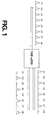
- Figure 1 is a conceptual illustration of a conversion from an optical channel scheme having 100 GHz spacing to an optical channel scheme having 200 GHz.
- the conversion of Figure 1 is useful, for example, to allow devices designed to operate with an optical channel scheme having 200 GHz channel spacing to interact with other devices or a network designed to operate with an optical channel scheme having 100 GHz channel spacing. Conversion between 100 GHz channel spacing and 200 GHz channel spacing allows, for example, network bandwidth to be increased without upgrading all of the devices that interact with the network.
- the converter of Figure 1 is a deinterleaver that separates an optical signal having even and odd channels (e.g., ITU channels) into a first optical signal including the even channels and a second optical signal including the odd signals.
- the odd channels have a 200 GHz spacing and the even channels have a 200 GHz spacing.
- Recombining the even and the odd channels can be accomplished with an interleaver that combines the odd channels and the even channels into a single optical signal.
- the even and odd channels having 200 GHz spacing are combined (interleaved) into an optical signal having 100 GHz signal spacing.
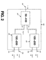
- FIG. 2 is a block diagram of an optical deinterleaver for conversion from an optical channel scheme having 50 GHz spacing to an optical channel scheme having 200 GHz spacing.
- deinterleaver 200 includes deinterleaver 210 to convert from one set of 50 GHz spaced channels to two sets of 100 GHz spaced channels.
- Deinterleaver 200 also includes two deinterleavers (220 and 230) each of which convert one of the sets of 100 GHz spaced channels to two sets of 200 GHz spaced channels.
- Deinterleaver 200 allows devices designed for 200 GHz spaced channels to interact with devices or networks designed for 50 GHz spaced channels.
- Optical fiber 205 carries a set of optical channels, i , having 50 GHz spacing.
- Deinterleaver 210 separates the set of optical channels into sets of even, 2( j +1 ), and odd, 2 j +1 , channels.
- the even channels are input to deinterleaver 230 and the odd channels are input deinterleaver 220.
- the even and the odd channels have 100 GHz spacing.
- Deinterleavers 220 and 230 operate to further separate the set of optical channels.
- deinterleaver 220 and 230 operate on the respective 100 GHz spaced channels to separate the input channels into "even” and “odd” channels.
- the sets of channels output by deinterleavers 220 and 230 have 200 GHz spacing.
- Deinterleaver 220 separates the odd channels into two sets of channels, odd-odd channels, 4 k +1 , output by optical fiber 240 and odd-even, 4 k +2 , channels output by optical fiber 250.
- Deinterleaver 230 separates the even channels into two sets of channels, the even-odd, 4 k +3 , channels output by optical fiber 260 and the even-even, 4( k +1) , channels output by optical fiber 270.
- the four sets of channels output by deinterleaver 200 are 200 GHz spaced channels.
- deinterleaver 200 can be used to interface one or more devices designed to operate on 200 GHz spaced channels with one or more devices or networks designed to operate on 50 GHz spaced channels.
- FIG. 3 is a block diagram of an optical interleaver for conversion from an optical channel scheme having 200 GHz spacing to an optical channel scheme having 50 GHz spacing.
- interleaver 300 includes interleaver 310 to convert from two sets of 200 GHz spaced channels to one set of 100 GHz spaced channels.
- interleaver 320 converts from two sets of 200 GHz spaced channels to one set of 100 GHz channels.
- Interleaver 330 converts the two sets of 100 GHz spaced channels to one set of 50 GHz spaced channels.
- Interleayer 300 allows devices designed for 200 GHz spaced channels to interact with devices or networks designed for 50 GHz spaced channels.
- the odd-odd, 4 k +1 , channels having 200 GHz spacing are input to interleaver 310 via optical fiber 340.
- the odd-even, 4 k +2 , channels having 200 GHz spacing are input to interleaver 310 via optical fiber 350.
- Interleaver 310 interleaves the odd-odd channels and the odd-even channels to generate a set of odd, 2 j +1 , channels having 100 GHz spacing.
- the even--odd, 4 k +3 , channels having 200 GHz spacing are input to interleaver 320 via optical fiber 360.
- the even-even, 4( k +1) , channels having 200 GHz spacing are input to interleaver 320 via optical fiber 370.
- Interleaver 320 interleaves the even-odd channels and the even-even channels to generate a set of even, 2( j +1) , channels having 100 GHz spacing.
- Interleaver 330 interleaves the even and odd channels to generate a set of channels, i , having 50 GHz spacing.
- interleaver 300 allows devices designed to operate on optical channels having 200 GHz spacing to interact with devices designed to operate on optical channels having 50 GHz spacing.
- Other channels spacings can also be supported.
- Figure 4a illustrates one embodiment of a single-pass folded interleaver/de-interleaver having input and output ports on a common side of the device. The arrows of Figure 4 correspond to the single-pass folded interleaver/deinterleaver operating as a deinterleaver.
- an optical signal carrying information on multiple frequencies for example, a wavelength division multiplexed (WDM) signal is receives and separated into two optical signals, each of which include a predetermined subset of frequencies (e.g., even channels and odd channels) from the input optical signal.
- WDM wavelength division multiplexed
- port 400 is a collimator assembly having a GRIN lens to collimate the light. Other types of lenses can also be used, or pre-collimated light can be received. Port 400 receives an optical signal via an optical fiber and collimates the optical signal with the GRIN lens.
- port 400 also includes half wave plate 402 to rotate either the vertically polarized component or the horizontally polarized component of the optical signal.
- half wave plate 402 has an azimuth angle of 45° with respect to an optical signal received by port 400 from optical fiber 404.
- the walk-off crystal of port 400 offsets the vertically polarized component of the optical signal and half wave plate 402 causes the vertically polarized component to be horizontally polarized such that both components are horizontally polarized.
- the collimated optical signal is directed to reflective element 410.
- reflective element 410 is a 90° reflecting crystal; however, other reflective elements can be used based on, for example, the physical layout of the interleaver/de-interleaver.
- the face(s) through which the optical signal is received and/or reflected has low-order compensator 480 component to compensate for phase shift in the respective crystals. If the reflective element does not cause a phase shift, low-order compensator 480 can be omitted.
- Half wave plate 430 introduces a relative phase difference of 180° between the ordinary and extraordinary components of the optical signal.
- half wave plate 430 is oriented with a first predetermined azimuth angle.
- the first azimuth angle is in the range of 0° to 10° (e.g., 3.5°) for optical signals passing from reflective element 410 to birefringent assembly 420; however, the azimuth angle can be different with appropriate changes to the angles of one or more other half wave plates.
- birefringent assembly 420 is composed of crystals 424 and 426 that are selected to provide improved thermal stability over a range of operating temperatures as compared to a single birefringent crystal.
- crystal 424 is a TiO 2 crystal having a thickness of approximately 2 mm
- crystal 426 is a YVO 4 crystal having a thickness of approximately 9.5 mm.
- birefringent assembly 420 has a cross sectional area that is 5 mm by 8 mm; however, other sizes can also be used.
- Other birefringent assemblies can also be used, for example, a single crystal can be used if temperature stability is not important, or other two-crystal birefringent assemblies can be used.
- the optical signal After passing through birefringent assembly 420, the optical signal is reflected by reflective element 412 back through birefringent assembly 420.
- reflective element 412 is a 90° reflecting crystal; however, other reflective elements can be used.
- the face(s) through which the optical signal is received and/or reflected has low-order compensator 482 to compensate for phase shift in the respective crystals. If the reflective element does not cause a phase shift, low-order compensator 482 can be omitted.
- half wave plate 432 After passing through birefringent assembly 420 as reflected by reflective element 412, the optical signal passes through half wave plate 432.
- half wave plate 432 is oriented with the first azimuth angle (e.g., 3.5°) for optical signals passing from birefringent assembly 420 to reflective element 414.
- Other azimuth angles for half wave plate 432 or for both half wave plate 432 and half wave plate 430 can be used for different filtering characteristics or physical configurations.
- the optical signal After passing through half wave plate 432, the optical signal is reflected by reflective element 414.
- reflective element 414 is a 90° reflecting crystal; however, other reflective elements can be used.
- the face(s) through which the optical signal is received and/or reflected has low-order compensator 484 to compensate for phase shift in the respective crystals. If the reflective element does not cause a phase shift, low-order compensator 484 can be omitted.
- half wave plate 434 is oriented with a second predetermined azimuth angle.
- the second azimuth angle is in the range of 0° to -10° (e.g., -9°) with respect to an optical signal that passes from reflective element 404 to birefringent assembly 420; however, the azimuth angle can be different with appropriate changes to the azimuth angles of one or more other half wave plates.
- the optical signal After passing through birefringent assembly 420, the optical signal is reflected by reflective element 416 back through birefringent assembly 420.
- reflective element 416 is a 90° reflecting crystal; however, other reflective elements can be used.
- the face(s) through which the optical signal is received and/or reflected has low-order compensator 486 to compensate for phase shift in the respective crystals. If the reflective element does not cause a phase shift, low-order compensator 486 can be omitted.
- half wave plate 436 After passing through birefringent assembly 420 as reflected by reflective element 416, the optical signal passes through half wave plate 436.
- half wave plate 436 is oriented with the second azimuth angle (e.g., -9°) with respect to optical signals that pass from birefringent assembly 420 to reflective element 418.
- Other azimuth angles for half wave plate 436 or for half wave plate 436 and half wave plate 434 can be used for different filtering characteristics or physical configurations.
- the optical signal After passing through half wave plate 436, the optical signal is reflected by reflective element 418.
- reflective element 418 is a 90° reflecting crystal; however, other reflective elements can be used.
- the face(s) through which the optical signal is received and/or reflected has low-order compensator 488 to compensate for phase shift in the respective crystals. If the reflective element does not cause a phase shift, low-order compensator 488 can be omitted.
- the optical signal reflected by reflective element 418 is directed through half wave plate 438.
- half wave plate 438 is oriented with a third predetermined azimuth angle.
- the third azimuth angle is 22.5° with respect to optical signals that pass from reflective element 418 to birefringent assembly 420.
- the azimuth angle of half wave plate 438 is -22.5° with respect to optical signals that pass from reflective element 418 to birefringent assembly 420.
- half wave plate 440 After passing through birefringent assembly 420, the optical signal passes through half wave plate 440.
- half wave plate 440 is oriented with the third predetermined azimuth angle (e.g., 22.5°) with respect to optical signals that pass from birefringent assembly 420 to beam splitter 450.
- half wave plate 440 has an azimuth angle of-22.5° with respect to optical signals that pass from birefringent assembly 420 to beam splitter 450.
- the azimuth angles of half wave plates 438 and 440 determine the ports to which the optical signals are directed. If the azimuth angles of half wave plates 438 and 440 are 22.5°, a first set of optical signals (e.g., even channels) is directed to port 470 and a second set of optical signals (e.g., odd channels) is directed to port 472. If the azimuth angles are -22.5°, the first set of optical signals is directed to port 470 and the second set of optical signals is directed to port 472.
- half wave plates 470 and 472 can be used to provide a switching function.
- half wave plates 470 and 172 are mechanically movable components.
- half wave plates 470 and 472 are voltage-controlled liquid crystal components where the voltage can be used to control the switching state of the components.
- the optical signal then passes through polarization beam splitter 450.
- the polarization beam splitter provides output signals to two output collimators.
- Polarization beam splitter 450 splits the optical signal based on polarization.
- the optical signal is split into a horizontally polarized signal and a vertically polarized signal.
- One output signal e.g., the horizontally polarized signal
- the second output signal e.g., the vertically polarized signal
- Other beam splitting components can also be used.
- Port 470 includes half wave plate 476 and port 472 includes half wave plate 474.
- both half wave plate 474 and half wave plate 476 have azimuth angles of 45° with respect to optical signals received from walk-off crystal 482 and walk-off crystal 450, respectively.
- Half wave plate 474 and 476 rotate the optical components received such that ports 472 and 470, respectively, each receive a vertically polarized component and a horizontally polarized component, which are combined and directed to optical fibers 473 and 475, respectively.
- one of ports 470 and 472 receives even ITU channels and the other port receives odd ITU channels.
- Other filtering characteristics can also be provided.
- a first block of channels e.g., 1-4
- a second block of channels e.g., 5-8
- two sets of optical signals are input to ports 470 and 472.
- the two sets of optical signals are combined in a manner that is the reverse of the deinterleaver function described above.
- the combined (interleaved) optical signal is output through port 400.
- the apparatus illustrated in Figure 4 can operate as an interleaver or as a deinterleaver.
- the interleaver/deinterleaver of Figure 4a is angle tuned to compensate for manufacturing tolerances.
- angle tuning is accomplished by rotating birefringent assembly 420 after the interleaver/deinterleaver has been assembled so that the signals (e.g., ITU channels) interleaved or deinterleaved match the desired characteristics.
- Birefringent assembly 420 is rotated to increase the optical path length of the signals passing through birefringent assembly 420.
- birefringent assembly 420 is maintained in the desired position through, for example, use of epoxy or soldering techniques.
- Figure 4b illustrates one embodiment of a single-pass folded interleaver/de-interleaver having input and output ports on a common side of the device.
- the interleaver/deinterleaver of Figure 4b includes the same components (e.g., reflective elements, half wave plates, birefringent assembly) as the interleaver/deinterleaver of Figure 4a; however, the components are arranged in different physical positions for the interleaver/deinterleaver of Figure 4b compared to the interleaver/deinterleaver of Figure 4a.
- the interleaver/deinterleaver of Figure 4b does not include the low-order compensators of the interleaver/deinterleaver of Figure 4a.
- the optical compensation of the low-order compensators can be provided by angle tuning birefringent assembly 420.
- the increase optical path length through material of the interleaver/deinterleaver can be provided by birefringent assembly 420 rather than by the low-order compensators.
- the interleaver/deinterleaver of Figure 4b can include low-order compensators as described above with respect to Figure 4a.
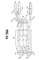
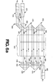
- Figure 5a illustrates one embodiment of a single-pass folded interleaver/deinterleaver having input and output ports on a common side of the device.
- the arrows of Figure 5 correspond to the single-pass folded interleaver/de-interleaver operating as a deinterleaver.
- the interleaver/deinterleaver of Figure 5 has three reflective elements rather than the five reflective elements of the interleaver/deinterleaver of Figure 4.
- port 500 is a collimator assembly having a GRIN lens to collimate the light. Other types of lenses can also be used, or pre-collimated light can be received.
- port 500 includes a walk-off crystal and half wave plate 502. The walk-off crystal and half wave plate 502 operate to provide two horizontally (or two vertically) polarized components.
- the optical signal is passed through polarizer 510.
- the polarization provided by polarizer 510 is in the range of 0° to 10° (e.g., 2.6°) for optical signals that pass from port 500 to reflective element 520, however, other polarizations can be provided based on, for example, the azimuth angles of one or more half wave plates.
- the polarized optical signal is directed to reflective element 520.
- reflective element 520 is a 90° reflecting crystal; however, other reflective elements can be used.
- the face(s) through which the optical signal is received and/or reflected has low-order compensator 530 component to compensate for phase shift in the respective crystals. If the reflective element does not cause a phase shift, low-order compensator 530 can be omitted.
- the optical signal reflected by reflective element 520 is directed through half wave plate 540.
- half wave plate 540 is oriented with a first predetermined azimuth angle.
- the first azimuth angle is in the range of 0° to -10° (e.g.,-6.7°) with respect to optical signals that pass from reflective element 520 to birefringent assembly 550; however, the azimuth angle can be different with appropriate changes to the azimuth angles of one or more other half wave plates and/or polarizer 510.
- birefringent assembly 520 is composed of crystals 524 and 526 that are selected to provide improved thermal stability over a range of operating temperatures as compared to a single birefringent crystal.
- crystal 524 is a TiO 2 crystal having a thickness of 2 mm
- crystal 526 is a YVO 4 crystal having a thickness of 9.5 mm.
- birefringent assembly 550 has a 6 mm by 5 mm cross sectional area; however, other sizes can also be used.
- Other birefringent assemblies can also be used, for example, a single crystal can be used if temperature stability is not important, or other two-crystal birefringent assemblies can be used.
- the optical signal After passing through birefringent assembly 550, the optical signal is reflected by reflective element 522 back through birefringent assembly 550.
- reflective element 522 is a 90° reflecting crystal; however, other reflective elements can be used.
- the face(s) through which the optical signal is received and/or reflected has low-order compensator 532 to compensate for phase shift in the respective crystals. If the reflective element does not cause a phase shift, low-order compensator 532 can be omitted.
- half wave plate 542 After passing through birefringent assembly 550 as reflected by reflective element 524, the optical signal passes through half wave plate 542.
- half wave plate 542 is oriented with the first azimuth angle (e.g., -6.7°) with respect to optical signals that pass from birefringent assembly 542 to reflective element 524.
- Other azimuth angles can be used for half wave plate 542 or for half wave plate 542 and half wave plate 540 for different filtering characteristics or physical configurations.
- the optical signal After passing through half wave plate 542, the optical signal is reflected by reflective element 524.
- reflective element 524 is a 90° reflecting crystal; however, other reflective elements can be used.
- the face(s) through which the optical signal is received and/or reflected has low-order compensator 534 to compensate for phase shift in the respective crystals. If the reflective element does not cause a phase shift, low-order compensator 534 can be omitted.
- the optical signal reflected by reflective element 524 is directed through half wave plate 544.
- half wave plate 544 is oriented with a second predetermined azimuth. In one embodiment, the second azimuth angle is 22.5°. In an alternate embodiment, the azimuth angle is -22.5°
- the optical signal passes through half wave plate 546.
- half wave plate 546 is oriented with an azimuth angle of 22.5°. In an alternate embodiment, the azimuth angle is -22.5°
- the azimuth angles of half wave plates 544 and 546 determine the ports to which the optical signals are directed.
- half wave plates 570 and 572 can be used to provide a switching function.
- half wave plates 570 and 572 are mechanically movable components.
- half wave plates 570 and 572 are voltage-controlled liquid crystal components where the voltage can be used to control the switching state of the components.
- the optical signal then passes through polarization beam splitter 565.
- the polarization beam splitter feeds two output collimators.
- Polarization beam splitter 565 splits the optical signal based on polarization.
- the optical signal is split into a horizontally polarized signal and a vertically polarized signal.
- One output signal e.g., the horizontally polarized signal
- the second output signal e.g., the vertically polarized signal
- Reflects 570 and 572 focus the output signals to an optical fiber.
- one of ports 570 and 572 receives even ITU channels and the other port receives odd ITU channels. Other filtering characteristics can also be provided.
- ports 570 and 572 include walk-off crystals and half wave plates 575 and 577, respectively, to one component of the optical signal received.
- the interleaver/deinterleaver of Figure 5a is angle tuned to compensate for manufacturing tolerances. In one embodiment, angle tuning is accomplished by rotating birefringent assembly 550 as described above with respect to birefringent assembly 420 of Figure 4a.
- FIG. 5 illustrates one embodiment of a single-pass folded interleaver/ deinterleaver having input and output ports on a common side of the device.
- the interleaver/deinterleaver of Figure 5b includes the same components (e.g., polarizer, reflective elements, half wave plates, birefringent assembly) as the interleaver/deinter-leaver of Figure 5a; however, the components are arranged in different physical positions for the interleaver/deinterleaver of Figure 5b compared to the interleaver/deinterleaver of Figure 5a.
- components e.g., polarizer, reflective elements, half wave plates, birefringent assembly
- the interleaver/deinterleaver of Figure 5b does not include the low-order compensators of the interleaver/deinterleaver of Figure 5a.
- the optical compensation of the low-order compensators can be provided by angle tuning birefringent assembly 550.
- the increase optical path length through material of the interleaver/deinterleaver can be provided by birefringent assembly 550 rather than by the low-order compensators.
- the interleaver/deinterleaver of Figure 5b can include low-order compensators as described above with respect to Figure 5a.
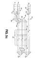
- Figure 5c illustrates one embodiment of a single-pass folded interleaver/ deinterleaver having input and output ports on a common side of the device.
- the interleaver/deinterleaver of Figure 5c includes the same components (e.g., reflective elements, half wave plates, birefringent assembly) as the interleaver/deinterleavers of Figures 5a and 5b with one exception.
- Half wave plate 580 replaces polarizer 510 and half wave plate 540 of Figures 5a and 5b.
- the remaining components are arranged in different physical positions for the interleaver/deinterleaver of Figure 5c compared to the interleaver/deinterleaver of Figures 5a and 5b.
- half wave plate 580 has an azimuth angle of -8° with respect to optical signals that pass from port 500 to reflective element 520; however, other angles could also be used.
- the interleaver/deinterleaver of Figure 5c does not include the low-order compensators of the interleaver/deinterleaver of Figure 5a.
- the optical compensation of the low-order compensators can be provided by angle tuning birefringent assembly 550.
- the increase optical path length through material of the interleaver/deinterleaver can be provided by birefringent assembly 550 rather than by the low-order compensators.
- the interleaver/deinterleaver of Figure 5c can include low-order compensators as described above with respect to Figures 5a and 5b.
- Figure 6a illustrates one embodiment of a single-pass folded interleaver/de-interleaver having input and output ports on opposite sides of the device. As with Figures 4 and 5 above, the arrows of Figure 6 correspond to the single-pass folded interleaver/de-interleaver operating as a deinterleaver.
- port 600 is a collimator assembly having GRIN lens to collimate the light. Other types of lenses can also be used, or pre-collimated light can be received.
- port 600 includes a walk-off crystal and half wave plate 602. The walk-off crystal and half wave plate 602 operate to provide two horizontally (or two vertically) polarized components.
- the collimated optical signal is directed through half wave plate 630.
- half wave plate 630 is oriented with a first predetermined azimuth angle.
- the angle is in the range of 0° to 10° (e.g., 3.5°) with respect to optical signals that pass from port 600 to birefringent assembly 620; however, the azimuth angle can be different with appropriate changes to the azimuth angles of one or more other half wave plates.
- birefringent assembly 620 is composed of crystals 624 and 626 that are selected to provide thermal stability over a range of operating temperatures.
- crystal 624 is a TiO 2 crystal having a thickness of 2 mm
- crystal 626 is a YVO 4 crystal having a thickness of 9.5 mm.
- Other birefringent assemblies can also be used.
- the optical signal After passing through birefringent assembly 620, the optical signal is reflected by reflective element 612 back through birefringent assembly 620.
- reflective element 612 is a 90° reflecting crystal; however, other reflective elements can be used.
- the face(s) through which the optical signal is received and/or reflected has low-order compensator 682 to compensate for phase shift in the respective crystals. If the reflective element does not cause a phase shift, low-order compensator 682 can be omitted.
- half wave plate 632 After passing through birefringent assembly 620 as reflected by reflective element 612, the optical signal passes through half wave plate 632.
- half wave plate 632 is oriented with the first azimuth angle (e.g., 3.5°) with respect to optical signals that pass from birefringent assembly 620 to reflective element 614.
- Other azimuth angles can be used half wave plate 632 or for half wave plate 632 and half wave plate 630 for different filtering characteristics or physical configurations.
- the optical signal After passing through half wave plate 632, the optical signal is reflected by reflective element 614.
- reflective element 614 is a 90° reflecting crystal; however, other reflective elements can be used.
- the face(s) through which the optical signal is received and/or reflected has low-order compensator 684 to compensate for phase shift in the respective crystals. If the reflective element does not cause a phase shift, low-order compensator 684 can be omitted.
- the optical signal reflected by reflective element 614 is directed through half wave plate 634.
- half wave plate 634 is oriented with a second predetermined azimuth angle .
- the second azimuth angle is in the range of 0° to -10° (e.g., -9°) with respect to optical signals that pass from reflective element 614 to birefringent assembly 620; however, the azimuth angle can be different with appropriate changes to the angles of one or more other half wave plates.
- the optical signal After passing through birefringent assembly 620, the optical signal is reflected by reflective element 616 back through birefringent assembly 620.
- reflective element 616 is a 90° reflecting crystal; however, other reflective elements can be used.
- the face(s) through which the optical signal is received and/or reflected has low-order compensator 686 to compensate for phase shift in the respective crystals. If the reflective element does not cause a phase shift, low-order compensator 686 can be omitted.
- half wave plate 636 After passing through birefringent assembly 620 as reflected by reflective element 616, the optical signal passes through half wave plate 636.
- half wave plate 636 is oriented with the third azimuth angle (e.g., -9°) with respect to optical signals that pass from birefringent assembly 620 to reflective element 618.
- Other azimuth angles can be used for half wave plate 636 or half wave plate 636 and half wave plate 634 for different filtering characteristics or physical configurations.
- the optical signal After passing through half wave plate 636, the optical signal is reflected by reflective element 618.
- reflective element 618 is a 90° reflecting crystal; however, other reflective elements can be used.
- the face(s) through which the optical signal is received and/or reflected has low-order compensator 688 to compensate for phase shift in the respective crystals. If the reflective element does not cause a phase shift, low-order compensator 688 can be omitted.
- the optical signal reflected by reflective element 618 is directed through half wave plate 638.
- half wave plate 638 is oriented with a third predetermined azimuth angle. In one embodiment, the third azimuth angle is 22.5°.
- the optical signal reflected by reflective element 618 is directed through half wave plate 638.
- half wave plate 638 is oriented with a second predetermined azimuth. In one embodiment, the second azimuth angle is 22.5°. In an alternate embodiment, the azimuth angle is -22.5°
- the optical signal passes through half wave plate 640.
- half wave plate 640 is oriented with an azimuth angle of 22.5°. In an alternate embodiment, the azimuth angle is -22.5° In one embodiment, the azimuth angles of half wave plates 638 and 640 determine the ports to which the optical signals are directed.
- half wave plates 670 and 672 can be used to provide a switching function.
- half wave plates 670 and 672 are mechanically movable components.
- half wave plates 670 and 672 are voltage-controlled liquid crystal components where the voltage can be used to control the switching state of the components.
- the optical signal After passing through birefringent assembly 620, the optical signal passes through half wave plate 640.
- half wave plate 640 is oriented with the third predetermined azimuth angle; however, other azimuth angles can also be used.
- the optical signal then passes through polarization beam splitter 650.
- the polarization beam splitter requires two output collimators.
- Polarization beam splitter 650 splits the optical signal based on polarization.
- the optical signal is split into a horizontally polarized signal and a vertically polarized signal.
- One output signal e.g., the horizontally polarized signal
- the second output signal e.g., the vertically polarized signal
- reflective element 660 which reflects the second output signal to port 672.
- Ports 670 and 672 focus the output signals to an optical fiber.
- one output signal includes even ITU channels and the other output signal includes odd ITU channels.
- ports 670 and 672 include walk-off crystals and half wave plates 675 and 677, respectively, to one component of the optical signal received.
- the interleaver/deinterleaver of Figure 6a is angle tuned to compensate for manufacturing tolerances. In one embodiment, angle tuning is accomplished by rotating birefringent assembly 620 as described above with respect to birefringent assembly 420 of Figure 4a.
- FIG. 6 illustrates one embodiment of a single-pass folded interleaver/de-interleaver having input and output ports on opposite sides of the device.
- the interleaver/deinterleaver of Figure 6b includes the same components (e.g., reflective elements, half wave plates, birefringent assembly) as the interleaver/deinterleaver of Figure 6a; however, the components are arranged in different physical positions for the interleaver/deinterleaver of Figure 6b compared to the interleaver/deinterleaver of Figure 6a.
- components e.g., reflective elements, half wave plates, birefringent assembly
- the interleaver/deinterleaver of Figure 6b does not include the low-order compensators of the interleaver/deinterleaver of Figure 6a.
- the optical compensation of the low-order compensators can be provided by angle tuning birefringent assembly 620.
- the increase optical path length through material of the interleaver/deinterleaver can be provided by birefringent assembly 620 rather than by the low-order compensators.
- the interleaver/deinterleaver of Figure 6b can include low-order compensators as described above with respect to Figure 6a.
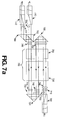
- Figure 7a illustrates one embodiment of a single-pass folded interleaver/de-interleaver having input and output ports on opposite sides of the device.
- the arrows of Figure 7 correspond to the single-pass folded interleaver/deinterleaver operating as a deinterleaver.
- the interleaver/deinterleaver of Figure 7 has three reflective elements rather than the five reflective elements of the interleaver/deinterleaver of Figure 6.
- port 700 is a collimator assembly having a GRIN lens to collimate the light. Other types of lenses can also be used, or pre-collimated light can be received.
- port 700 includes a walk-off crystal and half wave plate 702. The walk-off crystal and half wave plate 702 operate to provide two horizontally (or two vertically) polarized components.
- the optical signal is passed through polarizer 710.
- the polarization provided by polarizer 710 is in the range of 0° to 10° (e.g., 2.6°) with respect to optical signals that pass from port 700 to birefringent assembly 750; however, other polarizations can be provided based on, for example, the azimuth angles of one or more half wave plates.
- the polarized optical signal is directed through half wave plate 740.
- half wave plate 740 is oriented with a first predetermined azimuth angle.
- the angle is in the range of 0° to -10° (e.g., -6.7°) with respect to optical signals that pass from port 700 to birefringent assembly 750; however, the azimuth angle can be different with appropriate changes to the azimuth angles of one or more other half wave plates.
- birefringent assembly 750 is composed of crystals 754 and 756 that are selected to provide thermal stability over a range of operating temperatures.
- crystal 754 is a TiO 2 crystal having a thickness of 2 mm
- crystal 756 is a YVO 4 crystal having a thickness of 9.5 mm; however, other sizes can also be used.
- Other birefringent assemblies can also be used.
- the optical signal After passing through birefringent assembly 750, the optical signal is reflected by reflective element 722 back through birefringent assembly 750.
- reflective element 722 is a 90° reflecting crystal; however, other reflective elements can be used.
- the face(s) through which the optical signal is received and/or reflected has low-order compensator 732 to compensate for phase shift in the respective crystals. If the reflective element does not cause a phase shift, low-order compensator 732 can be omitted.
- half wave plate 742 After passing through birefringent assembly 750 as reflected by reflective element 724, the optical signal passes through half wave plate 742.
- half wave plate 742 is oriented with the first azimuth angle (e.g., -6.7°) with respect to optical signals that pass from birefringent assembly 750 to reflective element 724.
- Other azimuth angles can be used for half wave plate 742 or for half wave plate 742 and half wave plate 740 for different filtering characteristics or physical configurations.
- the optical signal After passing through half wave plate 742, the optical signal is reflected by reflective element 724.
- reflective element 724 is a 90° reflecting crystal; however, other reflective elements can be used.
- the face(s) through which the optical signal is received and/or reflected has low-order compensator 734 to compensate for phase shift in the respective crystals. If the reflective element does not cause a phase shift, low-order compensator 734 can be omitted.
- the optical signal reflected by reflective element 724 is directed through half wave plate 744.
- half wave plate 744 is oriented with a second predetermined azimuth angle.
- the second azimuth angle is 22.5°.
- the azimuth angle is -22.5°
- the optical signal passes through half wave plate 746.
- half wave plate 746 is oriented with an azimuth angle of 22.5° with respect to optical signals that pass from birefringent assembly 750 to beam splitter 765.
- the azimuth angle of half wave plate 746 is -22.5°.
- the azimuth angles of half wave plates 744 and 746 determine the ports to which the optical signals are directed. If the azimuth angles of half wave plates 744 and 746 are 22.5°, a first set of optical signals (e.g., even channels) is directed to port 770 and a second set of optical signals (e.g., odd channels) is directed to port 772. If the azimuth angles are -22.5°, the first set of optical signals is directed to port 770 and the second set of optical signals is directed to port 772.
- half wave plates 770 and 772 can be used to provide a switching function.
- half wave plates 770 and 772 are mechanically movable components.
- half wave plates 770 and 772 are voltage-controlled liquid crystal components where the voltage can be used to control the switching state of the components.
- the optical signal then passes through polarization beam splitter 765.
- the polarization beam splitter requires two output collimators.
- Polarization beam splitter 765 splits the optical signal based on polarization.
- the optical signal is split into a horizontally polarized signal and a vertically polarized signal.
- One output signal e.g., the horizontally polarized signal
- the second output signal e.g., the vertically polarized signal
- Ports 770 and 772 focus the output signals to an optical fiber.
- ports 770 and 772 include walk-off crystals and half wave plates 775 and 777, respectively, to one component of the optical signal received.
- the interleaver/deinterleaver of Figure 7a is angle tuned to compensate for manufacturing tolerances. In one embodiment, angle tuning is accomplished by rotating birefringent assembly 5750 as described above with respect to birefringent assembly 420 of Figure 4a.
- FIG. 7 illustrates one embodiment of a single-pass folded interleaver/de-interleaver having input and output ports on opposite sides of the device.
- the interleaver/deinterleaver of Figure 7b includes the same components (e.g., reflective elements, half wave plates, birefringent assembly) as the interleaver/deinterleaver of Figure 7a; however, the components are arranged in different physical positions for the interleaver/deinterleaver of Figure 7b compared to the interleaver/deinterleaver of Figure 7a.
- components e.g., reflective elements, half wave plates, birefringent assembly
- the interleaver/deinterleaver of Figure 7b does not include the low-order compensators of the interleaver/deinterleaver of Figure 7a.
- the optical compensation of the low-order compensators can be provided by angle tuning birefringent assembly 750.
- the increase optical path length through material of the interleaver/deinterleaver can be provided by birefringent assembly 750 rather than by the low-order compensators.
- the interleaver/deinterleaver of Figure 7b can include low-order compensators as described above with respect to Figure 7a.
- Figure 8a illustrates one embodiment of a cascaded folded interleaver/deinter-leaver having input and output ports on opposite sides of the device.
- the interleaver/ deinterleaver of Figure 8a is one embodiment of the block diagram of Figures 2 and 3.
- the arrows of Figure 8a corresponds to the deinterleaver of Figure 2.
- optical signals can be passed in the opposite direction of the arrows in Figure 8a.
- the interleaver/deinterleaver of Figure 8a includes three birefringent assemblies (820, 821 and 822). Optical signals that are received via port 800 are directed through birefringent assemblies 820, 821 and 822 to ports 890 and 892. Because the optical signals are not reflected back through birefringent assemblies 820, 821 and 822, the interleaver/deinterleaver of Figure 8a is a single-pass interleaver/deinterleaver.
- An optical signal received via port 800 is directed through half wave plate 831 and birefringent assembly 820, reflected by reflective element 810 back through birefringent assmbly 820, reflected by reflective element 811 through half wave plates 832 and 833, birefringent assembly 820 and half wave plates 834 and 835 to beam splitter 817.
- Beam splitter 817 splits the optical signals by polarization into a first sub-beam and a second sub-beam.
- the first sub-beam is passed through half wave plate 836, birefringent assembly 821, reflected by reflective element 814 back through birefringent assembly 821, reflected by reflective element 815 back through half wave plates 837 and 838, birefringent assembly 821 and half wave plates 843 and 844 to port 890.
- the second sub-beam is reflected by beam splitter 817 to reflective element 816, which directs the second sub-beam to half wave plate 845 to birefringent assembly 822, reflected by reflective element 813 back through birefringent assembly 822 to reflective element 812, which reflects the second sub-beam through half wave plates 839 and 840 to birefringent assembly 822 and half wave plates 841 and 842 to port 892.
- the azimuth angles of the half wave plates of the interleaver/deinterleaver of Figure 8a are chosen to separate even and odd ITU channels when an optical signal including both even and odd channels is received via port 800.
- the sets of channels are combined, or interleaved.
- one or more of birefringent assemblies 820, 821 and 822 is composed of two crystals that are selected to provide thermal stability over a range of operating temperatures.
- one crystal is a TiO 2 crystal having a thickness of 2 mm
- the second crystal is a YVO 4 crystal having a thickness of 9.5 mm; however, other sizes can also be used.
- Other birefringent assemblies can also be used, for example, a single crystal birefringent assembly.
- one or more of birefringent assemblies 820, 821 and 822 is angle tuned as described above.
- Figure 8b illustrates one embodiment of a cascaded folded interleaver/deinter-leaver having input and output ports on opposite sides of the device.
- the interleaver/deinterleaver of Figure 8b is one embodiment of the block diagram of Figures 2 and 3.
- the arrows of Figure 8b corresponds to the deinterleaver of Figure 2.
- optical signals can be passed in the opposite direction of the arrows in Figure 8b.
- the interleaver/deinterleaver of Figure 8b includes three birefringent assemblies (825 and 826). Optical signals that are received via port 800 are directed through birefringent assemblies 825 and 826 to ports 890 and 892. Because the optical signals are not reflected back through birefringent assemblies 825 and 826, the interleaver/deinterleaver of Figure 8b is a single-pass interleaver/deinterleaver.
- An optical signal received via port 800 passes through half wave plate 860 to birefringent assembly 825 and is reflected by reflective element 852 back through birefringent assembly 825 to reflective element 850, which reflects the optical signal through half wave plates 863 and 864, walk-off crystal 880, through half wave plates 865 and 866 to birefringent assembly 826, is reflected by reflective element 856 back through birefringent assembly 826 to reflective element 854, which reflects the signal through half wave plate 867 and 868 through birefringent assembly 826 and through half wave plates 869 and 870 to walk-off crystals 885 and 887.
- Walk-off crystals 885 and 887 direct one set of channels to port 890 and a second set of channels to port 892.
- the azimuth angles of the half wave plates of the interleaver/deinterleaver of Figure 8b are chosen to separate even and odd ITU channels when an optical signal including both even and odd channels is received via port 800.
- the sets of channels are combined, or interleaved.
- one or more of birefringent assemblies 825 and 826 is composed of two crystals that are selected to provide thermal stability over a range of operating temperatures.
- one crystal is a TiO 2 crystal having a thickness of 2 mm
- the second crystal is a YVO 4 crystal having a thickness of 9.5 mm; however, other sizes can also be used.
- Other birefringent assemblies can also be used, for example, a single crystal birefringent assembly.
- one or more of birefringent assemblies 825 and 826 is angle tuned as described above.
- interleaver/deinterleavers of Figures 8a and 8b are intended to represent two of the many possible single-pass cascaded interleaver/deinterlavers. Many alternative embodiments having two, three or more birefringent assemblies can be designed to provide a similar function. Thus, the invention as described with respect to cascaded single-pass interleaver/deinterleavers is not intended to be limited to the two embodiments illustrated in Figures 8a and 8b.
Landscapes
- Physics & Mathematics (AREA)
- General Physics & Mathematics (AREA)
- Optics & Photonics (AREA)
- Optical Communication System (AREA)
- Polarising Elements (AREA)
- Optical Modulation, Optical Deflection, Nonlinear Optics, Optical Demodulation, Optical Logic Elements (AREA)
Abstract
Description
Another disadvantage of multiple layers of thin film for filtering is that the thin films break down over time, especially when operating under high power conditions.
Figure 1 is a conceptual illustration of a conversion from an optical channel scheme having 100 GHz spacing to an optical channel scheme having 200 GHz. The conversion of Figure 1 is useful, for example, to allow devices designed to operate with an optical channel scheme having 200 GHz channel spacing to interact with other devices or a network designed to operate with an optical channel scheme having 100 GHz channel spacing. Conversion between 100 GHz channel spacing and 200 GHz channel spacing allows, for example, network bandwidth to be increased without upgrading all of the devices that interact with the network.
Figure 2 is a block diagram of an optical deinterleaver for conversion from an optical channel scheme having 50 GHz spacing to an optical channel scheme having 200 GHz spacing. In general,
The four sets of channels output by
Figure 3 is a block diagram of an optical interleaver for conversion from an optical channel scheme having 200 GHz spacing to an optical channel scheme having 50 GHz spacing. In general,
Figure 4a illustrates one embodiment of a single-pass folded interleaver/de-interleaver having input and output ports on a common side of the device. The arrows of Figure 4 correspond to the single-pass folded interleaver/deinterleaver operating as a deinterleaver. In other words an optical signal carrying information on multiple frequencies, for example, a wavelength division multiplexed (WDM) signal is receives and separated into two optical signals, each of which include a predetermined subset of frequencies (e.g., even channels and odd channels) from the input optical signal.
Figure 4b illustrates one embodiment of a single-pass folded interleaver/de-interleaver having input and output ports on a common side of the device. The interleaver/deinterleaver of Figure 4b includes the same components (e.g., reflective elements, half wave plates, birefringent assembly) as the interleaver/deinterleaver of Figure 4a; however, the components are arranged in different physical positions for the interleaver/deinterleaver of Figure 4b compared to the interleaver/deinterleaver of Figure 4a.
Figure 5a illustrates one embodiment of a single-pass folded interleaver/deinterleaver having input and output ports on a common side of the device. As with Figure 4, the arrows of Figure 5 correspond to the single-pass folded interleaver/de-interleaver operating as a deinterleaver. The interleaver/deinterleaver of Figure 5 has three reflective elements rather than the five reflective elements of the interleaver/deinterleaver of Figure 4.
Figure 5b illustrates one embodiment of a single-pass folded interleaver/ deinterleaver having input and output ports on a common side of the device. The interleaver/deinterleaver of Figure 5b includes the same components (e.g., polarizer, reflective elements, half wave plates, birefringent assembly) as the interleaver/deinter-leaver of Figure 5a; however, the components are arranged in different physical positions for the interleaver/deinterleaver of Figure 5b compared to the interleaver/deinterleaver of Figure 5a.
Figure 5c illustrates one embodiment of a single-pass folded interleaver/ deinterleaver having input and output ports on a common side of the device. The interleaver/deinterleaver of Figure 5c includes the same components (e.g., reflective elements, half wave plates, birefringent assembly) as the interleaver/deinterleavers of Figures 5a and 5b with one exception. Half wave plate 580 replaces
Figure 6a illustrates one embodiment of a single-pass folded interleaver/de-interleaver having input and output ports on opposite sides of the device. As with Figures 4 and 5 above, the arrows of Figure 6 correspond to the single-pass folded interleaver/de-interleaver operating as a deinterleaver.
Figure 6b illustrates one embodiment of a single-pass folded interleaver/de-interleaver having input and output ports on opposite sides of the device. The interleaver/deinterleaver of Figure 6b includes the same components (e.g., reflective elements, half wave plates, birefringent assembly) as the interleaver/deinterleaver of Figure 6a; however, the components are arranged in different physical positions for the interleaver/deinterleaver of Figure 6b compared to the interleaver/deinterleaver of Figure 6a.
Figure 7a illustrates one embodiment of a single-pass folded interleaver/de-interleaver having input and output ports on opposite sides of the device. As with Figures 4-6, the arrows of Figure 7 correspond to the single-pass folded interleaver/deinterleaver operating as a deinterleaver. The interleaver/deinterleaver of Figure 7 has three reflective elements rather than the five reflective elements of the interleaver/deinterleaver of Figure 6.
Figure 7b illustrates one embodiment of a single-pass folded interleaver/de-interleaver having input and output ports on opposite sides of the device. The interleaver/deinterleaver of Figure 7b includes the same components (e.g., reflective elements, half wave plates, birefringent assembly) as the interleaver/deinterleaver of Figure 7a; however, the components are arranged in different physical positions for the interleaver/deinterleaver of Figure 7b compared to the interleaver/deinterleaver of Figure 7a.
Figure 8a illustrates one embodiment of a cascaded folded interleaver/deinter-leaver having input and output ports on opposite sides of the device. The interleaver/ deinterleaver of Figure 8a is one embodiment of the block diagram of Figures 2 and 3. The arrows of Figure 8a corresponds to the deinterleaver of Figure 2. To implement the interleaver of Figure 3, optical signals can be passed in the opposite direction of the arrows in Figure 8a.
Figure 8b illustrates one embodiment of a cascaded folded interleaver/deinter-leaver having input and output ports on opposite sides of the device. As with Figure 8a, the interleaver/deinterleaver of Figure 8b is one embodiment of the block diagram of Figures 2 and 3. The arrows of Figure 8b corresponds to the deinterleaver of Figure 2. To implement the interleaver of Figure 3, optical signals can be passed in the opposite direction of the arrows in Figure 8b.
Claims (10)
- An interleaver or deinterleaver comprising:a first, a second and a third port;the first port being optically coupled with the second and third ports such that an optical signal launched into the first port is directed to the second and third ports;a first polarization beam splitter/combiner coupled with the first port for splitting the optical signal launched from the first port destined to the second and third ports into two sub-beams or for combining beams launched from the second and third ports destined to the first port into a single beam;a birefringent assembly including at least one birefringent plate optically coupled with the first, second and third ports; anda plurality of reflective elements optically coupled with the birefringent assembly to direct the sub-beams to follow optical paths that makes multiple passes through the birefringent assembly;a second polarization beam splitter/combiner coupled with the second and third ports for receiving light launched into the first port that has passed through the birefringent assembly a plurality of times for providing a first subset and a second subset of complementary channels to the second and third ports, respectively in a deinterleaveing mode of operation, and wherein the interleaver or deinterleaver for providing an interleaved signal at the first port when complementary channels are launched into the second and the third ports in an interleaving mode of operation.
- The interleaver or deinterleaver as defined in claim 1 wherein the birefringent assembly is comprised of at least two plates and wherein the plates are comprised of a different material to enhance thermal stability.
- The interleaver/deinterleaver of claim 1 or 2 further comprising one or more of half waveplates positioned between one or more of the reflective elements and the birefringent assembly, the one or more half wave plates being oriented with azimuth angles such that an optical signal passing through the birefringent assembly is rotated by the one or more half waveplates so that the polarization of the signal and birefringent axes of the birefringent assembly are varied between at least some multiple passes having the effect of launching a polarized beam through the birefringent assembly at a plurality of different polarization angles with respect to the axes of the assembly.
- The interleaver/deinterleaver of claim 3 wherein the plurality of half waveplates include a half wave plates oriented with a first azimuth angle, at least another half wave plates are oriented with a second azimuth angle and at least another half waveplate are oriented with a third azimuth angle.
- The interleaver/deinterleaver of claim 4 wherein the first azimuth angles are in the range of 0° to 10°,-5° to -15° and, 15° to 25°.
- The interleaver/deinterleaver of claim 2 comprising a polarizer, three reflective elements and four half wave plates.
- The interleaver/deinterleaver of claim 6 wherein the polarizer provides a polarization angle, two of the half wave plates are oriented with a first azimuth angle and two of the half wave plates are oriented with a second azimuth angle.
- The interleaver/deinterleaver of claim 1 wherein the birefringent assembly comprises a TiO2 crystal and a YVO4 crystal.
- The interleaver/deinterleaver of claim 1 wherein at least one of the reflective elements further comprise a low-order compensator component to compensate for a phase shift induced by at least one of the reflective elements.
- An interleaver / deinterleaver comprising:a plurality of birefringent plates;means for reflecting an optical signal such that the optical signal makes multiple passes through the plurality of birefringent plates, wherein a signal received via a first port is de-interleaved into a first subset and a second subset of complementary channels directed to a second port and a third port, respectively, and further wherein optical signals in the form of complementary channels received via the second port and the third port are combined and interleaved and directed to the first port.
Applications Claiming Priority (2)
| Application Number | Priority Date | Filing Date | Title |
|---|---|---|---|
| US09/476,609 US6337770B1 (en) | 1999-12-31 | 1999-12-31 | Single-pass folded interleaver/deinterleavers |
| US476609 | 1999-12-31 |
Publications (2)
| Publication Number | Publication Date |
|---|---|
| EP1115208A2 true EP1115208A2 (en) | 2001-07-11 |
| EP1115208A3 EP1115208A3 (en) | 2004-07-21 |
Family
ID=23892543
Family Applications (1)
| Application Number | Title | Priority Date | Filing Date |
|---|---|---|---|
| EP00311412A Withdrawn EP1115208A3 (en) | 1999-12-31 | 2000-12-19 | Single-pass folded interleaver/deinterleavers |
Country Status (4)
| Country | Link |
|---|---|
| US (1) | US6337770B1 (en) |
| EP (1) | EP1115208A3 (en) |
| CN (1) | CN1311262C (en) |
| CA (1) | CA2328747A1 (en) |
Cited By (1)
| Publication number | Priority date | Publication date | Assignee | Title |
|---|---|---|---|---|
| EP1508987A3 (en) * | 2003-08-18 | 2009-09-30 | Fujitsu Limited | Wavelength division multiplexing transmission system |
Families Citing this family (10)
| Publication number | Priority date | Publication date | Assignee | Title |
|---|---|---|---|---|
| US6459528B1 (en) * | 2000-05-23 | 2002-10-01 | Avanex Corporation | Optical passive components and bi-directional amplifier |
| US6704143B1 (en) | 2000-10-23 | 2004-03-09 | Adc Telecommunications, Inc. | Method and apparatus for adjusting an optical element to achieve a precise length |
| EP1333310A1 (en) * | 2000-11-10 | 2003-08-06 | Sumitomo Electric Industries, Ltd. | Interleaver, filter included therein, and interleaver system |
| US6717719B1 (en) * | 2001-10-01 | 2004-04-06 | The United States Of America As Represented By The Secretary Of The Air Force | Coherent optical beam combination using double-coated glass mirrors/mirror pairs |
| US7154659B1 (en) * | 2002-04-18 | 2006-12-26 | General Photonics Corporation | Optical depolarizers and DGD generators based on optical delay |
| US7092587B1 (en) | 2002-08-16 | 2006-08-15 | Raytheon Company | Multichannel optical demultiplexer with varying angles of incidence to the light bandpass filters |
| US20050281558A1 (en) * | 2004-06-18 | 2005-12-22 | Nec Laboratories America, Inc. | Flexible band tunable add/drop multiplexer and modular optical node architecture |
| US7723670B1 (en) | 2007-03-26 | 2010-05-25 | General Photonics Corporation | Optical differential group delay module with folded optical path |
| JP5617503B2 (en) * | 2010-09-30 | 2014-11-05 | 富士通株式会社 | Optical network repeater |
| US20240284080A1 (en) * | 2021-07-01 | 2024-08-22 | Francois Menard | Switched wavelength optical receiver for direct-detection methods and systems |
Family Cites Families (41)
| Publication number | Priority date | Publication date | Assignee | Title |
|---|---|---|---|---|
| US3503670A (en) * | 1967-01-16 | 1970-03-31 | Ibm | Multifrequency light processor and digital deflector |
| US4474435A (en) | 1981-12-07 | 1984-10-02 | Gte Laboratories Incorporated | Polarization-insensitive optical switch and multiplexing apparatus |
| US4474434A (en) | 1981-12-07 | 1984-10-02 | Gte Laboratories Incorporated | Polarization-insensitive optical switch apparatus |
| US4514046A (en) | 1981-12-07 | 1985-04-30 | Gte Laboratories Incorporated | Polarization-insensitive optical switch and multiplexing apparatus |
| US4464022A (en) | 1982-09-28 | 1984-08-07 | At&T Bell Laboratories | Optical circulator |
| US4685773A (en) | 1984-09-13 | 1987-08-11 | Gte Laboratories Incorporated | Birefringent optical multiplexer with flattened bandpass |
| US4566761A (en) | 1984-09-13 | 1986-01-28 | Gte Laboratories Incorporated | Birefringent optical wavelength multiplexer/demultiplexer |
| DE69121176T2 (en) | 1990-12-17 | 1997-01-09 | Nippon Telegraph & Telephone | Optical circulator |
| US5299056A (en) * | 1992-05-06 | 1994-03-29 | Matsushita Electric Industrial Co., Ltd. | Optical passive component assembly |
| US5499132A (en) * | 1992-05-13 | 1996-03-12 | Matsushita Electric Industrial Co., Ltd. | Optical passive components |
| JPH0667118A (en) * | 1992-08-20 | 1994-03-11 | Matsushita Electric Ind Co Ltd | Optical coupler |
| US5381250A (en) * | 1992-11-06 | 1995-01-10 | Displaytech, Inc. | Electro-optical switch with 4 port modules with electro-optic polarization rotators |
| US5319483A (en) * | 1992-12-04 | 1994-06-07 | Williams Telecommunications Group, Inc. | Polarization independent low cross-talk optical circulator |
| JP2986295B2 (en) * | 1992-12-08 | 1999-12-06 | 松下電器産業株式会社 | Optical isolator |
| US5493440A (en) * | 1993-10-19 | 1996-02-20 | Matsushita Electric Industrial Co., Ltd. | Optical isolator and optical fiber amplifier |
| US5471340A (en) | 1994-01-07 | 1995-11-28 | Jds Fitel Inc. | Reflective optical non-reciprocal devices |
| JP3153406B2 (en) * | 1994-03-03 | 2001-04-09 | 松下電器産業株式会社 | Optical circuit and optical transmission system using the same |
| US5488500A (en) | 1994-08-31 | 1996-01-30 | At&T Corp. | Tunable add drop optical filtering method and apparatus |
| US5852505A (en) | 1994-12-28 | 1998-12-22 | Lucent Technologies Inc. | Dense waveguide division multiplexers implemented using a first stage fourier filter |
| FR2731280B1 (en) | 1995-03-03 | 1997-04-04 | Hamel Andre | HIGH INSULATION INSERTION-EXTRACTION OPTICAL MULTIPLEXER |
| JPH08304664A (en) | 1995-05-09 | 1996-11-22 | Furukawa Electric Co Ltd:The | Wavelength demultiplexer |
| EP0840902B1 (en) * | 1995-07-27 | 2001-12-19 | Jds Fitel Inc. | Optical circulator |
| DE69620414T2 (en) | 1995-08-04 | 2002-11-14 | Alcatel, Paris | OPTICAL INSERT AND DISCONNECT MULTIPLEXER |
| JP3356365B2 (en) | 1995-09-19 | 2002-12-16 | ケイディーディーアイ株式会社 | Optical ADM device |
| US5689593A (en) * | 1995-10-13 | 1997-11-18 | E-Tek Dynamics, Inc. | Compact fiberoptic circulator with low polarization mode dispersion |
| US5808763A (en) | 1995-10-31 | 1998-09-15 | Jds Fitel Inc. | Optical demultiplexor |
| US5737104A (en) | 1995-12-18 | 1998-04-07 | Dicon Fiberoptics | Wavelength division multiplexer and demultiplexer |
| US5611004A (en) | 1996-01-30 | 1997-03-11 | Hewlett-Packard Company | Microphotonic polarization independent acousto optical tunable filter and receiver |
| US5724165A (en) * | 1996-07-23 | 1998-03-03 | Macro-Vision Communications, L.L.C. | Fault-tolerant optical routing switch |
| US5694233A (en) | 1996-07-23 | 1997-12-02 | Macro-Vision Communications, Llc | Switchable wavelength router |
| US5867291A (en) * | 1996-10-29 | 1999-02-02 | Chorum Technologies Inc. | Programmable wavelength router |
| US6005697A (en) * | 1996-07-23 | 1999-12-21 | Macro-Vision Communications, L.L.C. | Multi-wavelength cross-connect optical network |
| TW373080B (en) | 1996-09-04 | 1999-11-01 | Agilent Technologies Inc | Compact two-by-n optical components based on birefringent walk-off crystals |
| US5835517A (en) | 1996-10-04 | 1998-11-10 | W. L. Gore & Associates, Inc. | WDM multiplexer-demultiplexer using Fabry-Perot filter array |
| US5778118A (en) | 1996-12-03 | 1998-07-07 | Ciena Corporation | Optical add-drop multiplexers for WDM optical communication systems |
| JP4079228B2 (en) * | 1996-12-12 | 2008-04-23 | 富士通株式会社 | Optical device having optical circulator function |
| US5915051A (en) | 1997-01-21 | 1999-06-22 | Massascusetts Institute Of Technology | Wavelength-selective optical add/drop switch |
| US5926587A (en) | 1997-09-08 | 1999-07-20 | Lucent Technologies Inc. | Optical passband filters |
| US6002503A (en) | 1997-10-23 | 1999-12-14 | Ciena Corporation | Optical add/drop multiplexer |
| US5930039A (en) | 1997-12-08 | 1999-07-27 | U.S.A Kaifa Technology, Inc. | Optical circulator |
| US6075647A (en) * | 1998-01-30 | 2000-06-13 | Hewlett-Packard Company | Optical spectrum analyzer having tunable interference filter |
-
1999
- 1999-12-31 US US09/476,609 patent/US6337770B1/en not_active Expired - Lifetime
-
2000
- 2000-12-15 CA CA002328747A patent/CA2328747A1/en not_active Abandoned
- 2000-12-19 EP EP00311412A patent/EP1115208A3/en not_active Withdrawn
- 2000-12-29 CN CNB00137091XA patent/CN1311262C/en not_active Expired - Fee Related
Cited By (1)
| Publication number | Priority date | Publication date | Assignee | Title |
|---|---|---|---|---|
| EP1508987A3 (en) * | 2003-08-18 | 2009-09-30 | Fujitsu Limited | Wavelength division multiplexing transmission system |
Also Published As
| Publication number | Publication date |
|---|---|
| CN1311262C (en) | 2007-04-18 |
| CA2328747A1 (en) | 2001-06-30 |
| CN1348109A (en) | 2002-05-08 |
| EP1115208A3 (en) | 2004-07-21 |
| US6337770B1 (en) | 2002-01-08 |
Similar Documents
| Publication | Publication Date | Title |
|---|---|---|
| US6301046B1 (en) | Interleaver/deinterleavers causing little or no dispersion of optical signals | |
| US6169626B1 (en) | Optical signal interleaver | |
| US6847786B2 (en) | Compact wavelength filter using optical birefringence and reflective elements | |
| US6570711B2 (en) | Virtual waveplate and optical channel interleaver formed therewith | |
| US7058304B2 (en) | Bi-directional cross-connect | |
| US6337770B1 (en) | Single-pass folded interleaver/deinterleavers | |
| US6335830B1 (en) | Double-pass folded interleaver/deinterleavers | |
| US6587267B2 (en) | Beam directing device | |
| US6697198B2 (en) | Optical interleavers/deinterleavers | |
| US6845191B1 (en) | Optical filter for wavelength division multipled optical signals | |
| US6333816B1 (en) | Apparatus capable of operating as interleaver/deinterleavers or filters | |
| US6624939B2 (en) | 50/100 and 50/200 GHz de-interleaver with high isolation and dispersion compensation | |
| EP1136857A2 (en) | Interleaver/deinterleavers causing little or no dispersion of optical signals | |
| US6643063B2 (en) | Deinterleaver with high isolation and dispersion compensation and 50/200GHz interleaver and deinterleaver | |
| US6342968B1 (en) | Frequency tuning of optical devices | |
| US20020159151A1 (en) | Optical interleaver using mach-zehnder interferometry | |
| CA2359604C (en) | Optical interleavers/deinterleavers | |
| US6900938B2 (en) | Low dispersion interleaver | |
| WO2002043296A2 (en) | Birefringent interleaver for wdm fiber optic communications | |
| CA2328562A1 (en) | Multi-pass folded interleaver/deinterleavers | |
| JP2003255284A (en) | Variable optical gain equalizer | |
| US20030025998A1 (en) | Folding interleaver | |
| CA2330407A1 (en) | Modular interleaver/deinterleaver |
Legal Events
| Date | Code | Title | Description |
|---|---|---|---|
| PUAI | Public reference made under article 153(3) epc to a published international application that has entered the european phase |
Free format text: ORIGINAL CODE: 0009012 |
|
| AK | Designated contracting states |
Kind code of ref document: A2 Designated state(s): AT BE CH CY DE DK ES FI FR GB GR IE IT LI LU MC NL PT SE TR |
|
| AX | Request for extension of the european patent |
Free format text: AL;LT;LV;MK;RO;SI |
|
| RAP1 | Party data changed (applicant data changed or rights of an application transferred) |
Owner name: JDS UNIPHASE CORPORATION |
|
| RIC1 | Information provided on ipc code assigned before grant |
Ipc: 7G 02B 6/42 B Ipc: 7G 02B 6/26 B Ipc: 7G 02B 6/34 B Ipc: 7G 02B 27/28 B Ipc: 7H 03M 13/27 A |
|
| PUAL | Search report despatched |
Free format text: ORIGINAL CODE: 0009013 |
|
| AK | Designated contracting states |
Kind code of ref document: A3 Designated state(s): AT BE CH CY DE DK ES FI FR GB GR IE IT LI LU MC NL PT SE TR |
|
| AX | Request for extension of the european patent |
Extension state: AL LT LV MK RO SI |
|
| STAA | Information on the status of an ep patent application or granted ep patent |
Free format text: STATUS: THE APPLICATION IS DEEMED TO BE WITHDRAWN |
|
| 18D | Application deemed to be withdrawn |
Effective date: 20040701 |