EP1115120A2 - Method and apparatus for temperature compensation of read-only memory - Google Patents
Method and apparatus for temperature compensation of read-only memory Download PDFInfo
- Publication number
- EP1115120A2 EP1115120A2 EP00310932A EP00310932A EP1115120A2 EP 1115120 A2 EP1115120 A2 EP 1115120A2 EP 00310932 A EP00310932 A EP 00310932A EP 00310932 A EP00310932 A EP 00310932A EP 1115120 A2 EP1115120 A2 EP 1115120A2
- Authority
- EP
- European Patent Office
- Prior art keywords
- resistor
- voltage
- data
- recited
- temperature
- Prior art date
- Legal status (The legal status is an assumption and is not a legal conclusion. Google has not performed a legal analysis and makes no representation as to the accuracy of the status listed.)
- Withdrawn
Links
- 238000000034 method Methods 0.000 title claims abstract description 15
- 230000015654 memory Effects 0.000 title claims description 11
- 229910021420 polycrystalline silicon Inorganic materials 0.000 claims abstract description 20
- 229920005591 polysilicon Polymers 0.000 claims abstract description 19
- 230000008859 change Effects 0.000 claims description 13
- 239000000463 material Substances 0.000 claims description 11
- 229910044991 metal oxide Inorganic materials 0.000 claims description 2
- 150000004706 metal oxides Chemical class 0.000 claims description 2
- 230000007423 decrease Effects 0.000 abstract description 8
- 230000001419 dependent effect Effects 0.000 abstract description 5
- 230000004044 response Effects 0.000 abstract description 4
- 230000003247 decreasing effect Effects 0.000 abstract description 2
- 239000004065 semiconductor Substances 0.000 description 3
- 230000002411 adverse Effects 0.000 description 2
- 230000008901 benefit Effects 0.000 description 2
- 238000007620 mathematical function Methods 0.000 description 2
- 230000004048 modification Effects 0.000 description 2
- 238000012986 modification Methods 0.000 description 2
- 230000008569 process Effects 0.000 description 2
- ZOXJGFHDIHLPTG-UHFFFAOYSA-N Boron Chemical compound [B] ZOXJGFHDIHLPTG-UHFFFAOYSA-N 0.000 description 1
- 206010065929 Cardiovascular insufficiency Diseases 0.000 description 1
- 229910052787 antimony Inorganic materials 0.000 description 1
- WATWJIUSRGPENY-UHFFFAOYSA-N antimony atom Chemical compound [Sb] WATWJIUSRGPENY-UHFFFAOYSA-N 0.000 description 1
- 229910052785 arsenic Inorganic materials 0.000 description 1
- RQNWIZPPADIBDY-UHFFFAOYSA-N arsenic atom Chemical compound [As] RQNWIZPPADIBDY-UHFFFAOYSA-N 0.000 description 1
- 229910052796 boron Inorganic materials 0.000 description 1
- 230000000295 complement effect Effects 0.000 description 1
- 238000010586 diagram Methods 0.000 description 1
- 238000005516 engineering process Methods 0.000 description 1
- 230000005669 field effect Effects 0.000 description 1
- BHEPBYXIRTUNPN-UHFFFAOYSA-N hydridophosphorus(.) (triplet) Chemical compound [PH] BHEPBYXIRTUNPN-UHFFFAOYSA-N 0.000 description 1
- 239000011810 insulating material Substances 0.000 description 1
- 238000004519 manufacturing process Methods 0.000 description 1
- 229910052710 silicon Inorganic materials 0.000 description 1
- 239000010703 silicon Substances 0.000 description 1
Images
Classifications
-
- G—PHYSICS
- G11—INFORMATION STORAGE
- G11C—STATIC STORES
- G11C7/00—Arrangements for writing information into, or reading information out from, a digital store
- G11C7/04—Arrangements for writing information into, or reading information out from, a digital store with means for avoiding disturbances due to temperature effects
-
- G—PHYSICS
- G11—INFORMATION STORAGE
- G11C—STATIC STORES
- G11C17/00—Read-only memories programmable only once; Semi-permanent stores, e.g. manually-replaceable information cards
- G11C17/08—Read-only memories programmable only once; Semi-permanent stores, e.g. manually-replaceable information cards using semiconductor devices, e.g. bipolar elements
- G11C17/10—Read-only memories programmable only once; Semi-permanent stores, e.g. manually-replaceable information cards using semiconductor devices, e.g. bipolar elements in which contents are determined during manufacturing by a predetermined arrangement of coupling elements, e.g. mask-programmable ROM
Definitions
- This invention relates generally to electronic circuits and, more particularly, to temperature compensation of read-only-memory (ROM) electronic circuits.
- ROM read-only-memory
- ROMs Read-Only Memories
- ROMs are well known in the art.
- ROMs are used in computer systems to provide a permanent storage of program instructions, such as mathematical functions, or informational data that is processed by mathematical functions.
- a ROM typically consists of a planar array of parallel word lines, which are perpendicular to and insulated from a planar array of parallel bit lines.
- the two planes containing the word lines and bit lines are vertically disposed from each other and separated by an insulating layer.
- Active semiconductor devices such as bi-polar transistors or metal oxide semiconductor field effect transistors (MOSFETs) interconnect the junction of each word line and each bit line to form a memory cell.
- MOSFETs metal oxide semiconductor field effect transistors
- all the cells are populated with devices, and then a link to a particular device is opened in the encoding process to render that cell inactive.
- the connection or lack of connection of a device at a memory cell determines whether a logic "1" or "0" is stored in the cell.
- the control electrode (base or gate) of the active device is connected to the word line, and the emitter or source electrode is typically connected to the bit line, for transistor or MOSFET devices, respectively.
- a positive potential on a word line turns “on” the device at that cell. Where there is no physical link at the cell there is no signal transmitted to the bit line.
- the bit lines are then read in parallel to obtain a group of "I” and "0" signals that form the output of the ROM.
- ROM devices may also be fabricated with resistive interconnections.
- U.S. Patent 5,847,442 to Mills, et al ., entitled “Structure for Read-Only Memories,” which is incorporated by reference herein teaches a ROM device fabricated using resistive devices to interconnect word and bit lines. The use of resistive devices is advantageous over transistor devices as resistive devices are easier to fabricate and smaller in size. A brief summary of the incorporated reference is presented to provide a better understanding of the invention claimed herein.
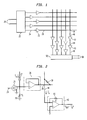
- FIG. 1 A ROM device fabricated with resistive devices is illustrated in Figure 1 of the referred to U.S. Patent and is repeated herein as Figure 1.
- resistive device 30 The connection between word line 28 and bit line 40 is specified by the specific data stored in the ROM device.
- Resistive device 30 is formed as a column, or post, within the insulating material that separates parallel word line 28 from the vertically disposed parallel bit line 40 .
- Resistive device 30 may be fabricated within a wide range of values. In order to reduce cross-talk between word line 28 and bit line 40 the minimum value of resistance is in the order of tens of Megaohms. To achieve resistive values in the order of tens of Megaohms in the space allocated, resistive device 30 is typically comprised of a polysilicon material having a controlled resistivity. Polysilicon materials are well known in the art and, as is known, may be formulated in a doped or undoped condition. Doping elements are typically selected from a group of elements consisting of boron, phosphorous, arsenic, and antimony.
- a significant advantage of using a polysilicon post as a resistor device to interconnect word and bits lines is a decrease in the size of a memory cell as resistive devices are smaller and required less power than transistors or MOSFETs.
- polysilicon is highly temperature sensitive, and, as is known in the art, the resistance of polysilicon decreases significantly with an increase in temperature. As the temperature increases and the resistivity of the connecting polysilicon resistive device decreases, the current through the resistive device increases. The increased current is known in the art to adversely affect the output voltage of the ROM as the output voltage is directly related to the current.
- One method of compensating for the increased output voltage is also disclosed in the aforementioned U.S. Patent. This method discloses using an operational amplifier with a gain characteristic responsive to the change in temperature as sense amplifier 42 . As disclosed, the operational amplifier employs a feedback resistor with electrical and thermal characteristics similar to those of data resistor 30 . In this method, the gain of the operational amplifier decreases as the resistance of the feedback resistor decreases. The decreased gain compensates for the increased data current and maintains the output voltage substantially constant.
- a disadvantage of this method of compensation is that the current flowing through the ROM device remains strongly related to the change in temperature. This change in current flow further affects the switching speed of the ROM device, and accordingly, the switching speed remains strongly influenced by the change in temperature.
- the present invention relates to temperature compensation of Read-Only Memory (ROM) that uses a temperature sensitive resistive material to connect word and bit lines.
- ROM Read-Only Memory
- the change in temperature adversely affects the output voltage and the switching speed of the ROM.
- the current through a data resistive device is maintained at a substantially constant level by supplying to the ROM an input reference voltage that is responsive to changes in temperature.
- an input reference voltage is developed by supplying a constant current source across a temperature-dependent reference resistor. The resistance of a reference resistor changes in response to changes in temperature and the voltage across the reference resistor (and input to the ROM) changes accordingly.
- the data current to the ROM data resistors remains substantially constant.
- the output voltage and ROM switching speed are maintained substantially constant.
- the reference resistor is made from a material that has a similar temperature-dependent resistivity as the material selected as the resistive device that interconnects word and bit lines within the ROM.
- a change in resistance of the reference resistor matches a change in resistance of the data resistor, thus causing the current flow through the data resistor to remain substantially constant for any change in temperature.
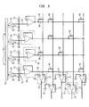
- switch 25 is used to translate a command on an input address line 24 to a voltage on word line 28 .
- a MOSFET switch is used to translate an address line command to a word line voltage.
- CMOS complementary metal-oxide-semiconductor
- diodes diodes
- electro-static switches may be used in accordance with the invention.
- switch 25 when switch 25 is gated high ( i .
- driver 26 is represented as an unity gain operational amplifier configured as a voltage follower. As is known in the art, the voltage V i at the high impedance input of the amplifier is present at the low impedance output of the amplifier. Hence, the reference voltage is present at the input side of data resistor 30 .
- reference resistor 29 is a temperature-dependent resistor having similar properties of conductivity as data resistor 30 .
- the resistive value of reference resistor 29 changes and the voltage developed across reference resistor changes in direct relation to the change in resistance.
- data resistor 30 and reference resistor 29 have the same electrical and thermal characteristics, upon gating switch 25 off the driver voltage V r appears on word line 25 and current I a flows from an input line (word line 28 ) to an output line (bit line 40 ) through data resistor 30 .
- Current I a is then supplied to sense amplifier 42 to produce an output voltage.
- reference resistor 29 is formed from a material with substantially similar properties of conductivity as those of data resistor 30 .
- the resistance values of data resistor 30 and reference resistor 29 change at substantially the same rate in response to a change in temperature. Accordingly, with constant current I a supplied to reference resistor 29 , the voltage developed across reference resistor 29 at any temperature is substantially the same as the voltage drop across data resistor 30 caused by current I a flowing through data resistor 30.
- the input reference voltage is thus adjusted at a rate that maintains current I a substantially constant through data resistor 30 when the associated word line is selected.
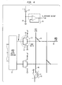
- FIG 3 illustrates one embodiment of the present invention incorporated in a resistive device ROM illustrated in Figure 1.
- a temperature compensation circuit of the type illustrated in Figure 2 is connected to each input word line 28 through driver amplifier 26 .
- inputs 20 provide commands to an n-stage ring counter 22 having a series of outputs connected to address lines 24 .
- Address lines 24 are then connected, in this illustrated embodiment to a series of MOSFET switches 25 , one switch for each address line. Coupled to each switch, is a reference resistor 29 .
- reference voltage V r is developed across reference resistor 29 by supplying a constant current to temperature-dependent reference resistor 29, when the illustrated switch 25 is gated low. When switch 25 is gated high, the reference voltage is nominally at ground level. Reference voltage V r is then used as input voltage V i to driver 26. Drivers 26 are typically in a low output state and each driver, when turned on, produces an output voltage V 0 that follows the input voltage, V i . In accordance with one embodiment of the invention, V i is either a nominally zero level when a selected MOSFET switch 25 is gated on or a nominally V r level when a selected MOSFET switch 25 is gated off.
- word line 28 is insulated from the bit line 40 except at selected cell sites where a connection is made between a word line and a bit line by data resistor 30 .
- current I a flows from word line 28 to bit line 40.
- Current I a is then conveyed sense amplifier 42 by bit line 40 .
- sense amplifier 42 is a feedback operational amplifier with a gain determined by feedback resistor 41 .
- sense amplifier 42 may be operated either in a linear or non-linear mode.
- feedback resistor 41 is a fixed value, and is substantially independent of temperature.
- the output voltage of sense amplifier 42 may then be determined from current I a and feedback resistor 41. As both the current I a and resistor 41 are temperature-independent, the output voltage remains substantially constant.
- FIG 4 illustrates a second embodiment of the invention as applied to a ROM device illustrated in Figure 1.
- a single constant current source 27 and reference resistor 29 are used to generate reference voltage V r .
- Reference voltage V r is then applied to each word line 28 through, in this illustrated embodiment, CMOS switch 25 .
- CMOS switch 25 is implemented as an inverter composed of two complementary MOSFET switches 62 and 64 .
- switch 64 when a selected address line 24 is high, switch 64 is gated off and switch 62 is gated on. Accordingly, the voltage level at the input to drive 26 and, correspondingly, word line 28 is nominally at a ground level.
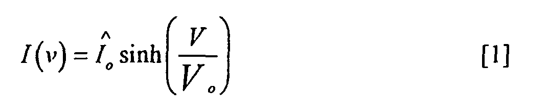
- Equation 1 it would be understood by one skilled in the art that when the voltage, V , is greater than V 0 , then the resistance in the polysilicon material is non-linear. A more detailed presentation of the properties of polysilicon materials may be found in Chapter 5 of "Polycrystalline Silicon for Integrated Circuit Applications,” Ted Kamins, Kluwer Academic Publishers, Boston, 1988. Furthermore, it is understood from Equations 1 and 2, that the current, I(v) , is exponentially related to the voltage and the inverse of temperature, therefore, large changes in resistive value are compensated by small changes in voltage. In still another embodiment of the invention, the current flowing through data resistor 30 may be proportional to the input current I a .
- the reference voltage, V r may be generated by analog or digital means from locally measured temperature. Further still, the reference voltage may be developed externally or internally to the ROM. In a preferred embodiment of the invention, polysilicon reference resistors and an analog method are used to generate the reference voltage.
Landscapes
- Read Only Memory (AREA)
Abstract
Description

Claims (21)
- In a ROM device using a plurality of data resistors to interconnect a plurality of input word lines with a plurality of output bit lines, a temperature compensation circuit to maintain a current through a selected one of said data resistors substantially constant comprising:at least one reference resistor, wherein the conductivity of said reference resistors is responsive to changes in temperature;a constant current source coupled to said at least one reference resistor, said constant current source developing a voltage across said at least one reference resistor; andat least one switch connected to said at least one reference resistor to selectively couple said voltage to said input word lines.
- A temperature compensation circuit as recited in Claim I wherein conductive properties of said reference resistor are selected to be the same as the conductive properties of said data resistors.
- A temperature compensation circuit as recited in Claim 1 wherein conductive properties of said reference resistor s are selected to be substantially similar to the conductive properties of said data resistors.
- A temperature compensation circuit as recited in Claim 2 or 3 wherein said data resistor is selected from a polysilicon material.
- A temperature compensation circuit as recited in Claim 4 wherein said polysilicon material is undoped.
- A temperature compensation circuit as recited in Claim 4 wherein said polysilicon material is doped.
- A temperature compensation circuit as recited in Claim 2 or 3 wherein said data resistor is comprised of a metal oxide.
- A method to maintain a current through Read-Only Memory (ROM) substantially constant as temperature changes wherein said ROM employs a plurality of data resistors to provide electrical interconnections between a plurality of input lines and output lines, comprising the steps of:selecting a reference resistor having substantially similar properties of conductivity as said data resistor;supplying a reference voltage to said input lines, said reference voltage developed by supplying a constant current to said reference resistor, wherein said reference voltage is responsive to a change in temperature.
- The method as recited in Claim 8 wherein said data resistor is comprised of undoped polysilicon
- The method as recited in Claim 8 wherein said data resistor is comprised of doped polysilicon.
- In a ROM device using a plurality of data resistors to interconnect a plurality of input word lines with a plurality of output bit lines, a temperature compensation circuit to maintain a current through a selected one of said data resistors substantially constant comprising:at least one voltage source producing a voltage that is responsive to changes in temperature; andat least one switch connected to said at least one voltage source to selectively couple said voltage to said input word lines.
- A temperature compensation circuit as recited in Claim 1 or 11 further comprising:
a plurality of sense amplifiers coupled to said output bit lines, each output line having at least one sense amplifier, said sense amplifier receiving said constant current flowing through said data resistors wherein each of said sense amplifier provides a constant output voltage. - A temperature compensation circuit as recited in Claim 12 wherein said sense amplifier comprises
an operational amplifier with a fixed feedback resistor, R, wherein said amplifier output voltage is determined from the value of said constant current and said feedback resistor. - A temperature compensation circuit as recited in Claim 13wherein said feedback resistor is temperature independent.
- A temperature compensation circuit as recited in Claim 12 wherein said sense amplifier is operated in the non-linear region.
- A temperature compensation circuit as recited in Claim 12 wherein said sense amplifier is operated in the linear region.
- A temperature compensation circuit as recited in Claim 1 or 11 wherein said at least one switch selectively couples said voltage to a selected one of said input word lines when an input to said switch is high.
- A temperature compensation circuit as recited in Claim 1 or 11 wherein said at least one switch selectively couples said voltage to a selected one of said input word lines when an input to said switch is low.
- A temperature compensation circuit as recited in claim 11 wherein said temperature responsive voltage changes to compensate for changes in voltage across said data resistor.
- A method to maintain a current through Read-Only Memory (ROM) substantially constant as temperature changes wherein said ROM employs a plurality of data resistors to provide electrical interconnections between a plurality of input lines and output lines, comprising the steps of:
supplying a reference voltage that is responsive to changes in temperature to said input lines, wherein said reference voltage changes to maintain said current through said data resistor substantially constant. - The method as recited in Claim 8 or 20 wherein the step of supplying said reference voltage further comprises the step of selectively switching said reference voltage to said word line.
Applications Claiming Priority (2)
| Application Number | Priority Date | Filing Date | Title |
|---|---|---|---|
| US479708 | 2000-01-07 | ||
| US09/479,708 US6762474B1 (en) | 1998-06-10 | 2000-01-07 | Method and apparatus for temperature compensation of read-only memory |
Publications (2)
| Publication Number | Publication Date |
|---|---|
| EP1115120A2 true EP1115120A2 (en) | 2001-07-11 |
| EP1115120A3 EP1115120A3 (en) | 2003-09-10 |
Family
ID=23905084
Family Applications (1)
| Application Number | Title | Priority Date | Filing Date |
|---|---|---|---|
| EP00310932A Withdrawn EP1115120A3 (en) | 2000-01-07 | 2000-12-08 | Method and apparatus for temperature compensation of read-only memory |
Country Status (2)
| Country | Link |
|---|---|
| EP (1) | EP1115120A3 (en) |
| JP (1) | JP2001236793A (en) |
Cited By (3)
| Publication number | Priority date | Publication date | Assignee | Title |
|---|---|---|---|---|
| EP1420412B1 (en) * | 2002-11-18 | 2008-07-09 | STMicroelectronics S.r.l. | Circuit and method for temperature tracing of devices including an element of chalcogenic material, in particular phase change memory devices |
| WO2013037659A1 (en) | 2011-09-12 | 2013-03-21 | Agfa Healthcare | Calibration free dual energy radiography method |
| EP2675151A1 (en) | 2012-06-11 | 2013-12-18 | Agfa Healthcare | A method to evaluate the presence of a source of x-ray beam inhomogeneity during x-ray exposure. |
Family Cites Families (4)
| Publication number | Priority date | Publication date | Assignee | Title |
|---|---|---|---|---|
| FR2071501A5 (en) * | 1969-12-31 | 1971-09-17 | Dondoux Jacques | |
| FR2644264B1 (en) * | 1989-03-10 | 1991-05-10 | Thomson Csf | PROGRAMMABLE ANALOGUE NEURONAL NETWORK |
| JP3705842B2 (en) * | 1994-08-04 | 2005-10-12 | 株式会社ルネサステクノロジ | Semiconductor device |
| US5847442A (en) * | 1996-11-12 | 1998-12-08 | Lucent Technologies Inc. | Structure for read-only-memory |
-
2000
- 2000-12-08 EP EP00310932A patent/EP1115120A3/en not_active Withdrawn
- 2000-12-28 JP JP2000401269A patent/JP2001236793A/en active Pending
Cited By (3)
| Publication number | Priority date | Publication date | Assignee | Title |
|---|---|---|---|---|
| EP1420412B1 (en) * | 2002-11-18 | 2008-07-09 | STMicroelectronics S.r.l. | Circuit and method for temperature tracing of devices including an element of chalcogenic material, in particular phase change memory devices |
| WO2013037659A1 (en) | 2011-09-12 | 2013-03-21 | Agfa Healthcare | Calibration free dual energy radiography method |
| EP2675151A1 (en) | 2012-06-11 | 2013-12-18 | Agfa Healthcare | A method to evaluate the presence of a source of x-ray beam inhomogeneity during x-ray exposure. |
Also Published As
| Publication number | Publication date |
|---|---|
| EP1115120A3 (en) | 2003-09-10 |
| JP2001236793A (en) | 2001-08-31 |
Similar Documents
| Publication | Publication Date | Title |
|---|---|---|
| US6762474B1 (en) | Method and apparatus for temperature compensation of read-only memory | |
| US11972830B2 (en) | Methods for accessing resistive change elements operable as antifuses | |
| US4146902A (en) | Irreversible semiconductor switching element and semiconductor memory device utilizing the same | |
| US6985027B2 (en) | Voltage step down circuit with reduced leakage current | |
| US20080217658A1 (en) | Electrical antifuse with integrated sensor | |
| US20030103401A1 (en) | Write current compensation for temperature variations in memory arrays | |
| KR20030033947A (en) | Semiconductor device | |
| JP2003173672A5 (en) | ||
| US5049970A (en) | High resistive element | |
| KR960012001A (en) | Semiconductor Memory with Improved Hierarchy of Power Supply Lines | |
| KR101440322B1 (en) | Integrated circuit fuse array | |
| TW200414673A (en) | An adjustable offset differential amplifier | |
| WO2010074904A1 (en) | Random access memory architecture including midpoint reference | |
| US4599554A (en) | Vertical MOSFET with current monitor utilizing common drain current mirror | |
| JPS638558B2 (en) | ||
| EP4095861B1 (en) | Memory read circuitry with a flipped voltage follower | |
| US20030058694A1 (en) | Temperature and voltage compensated reference current generator | |
| US7723820B2 (en) | Transistor based antifuse with integrated heating element | |
| US20050280495A1 (en) | Fuse-data reading circuit | |
| US20060002193A1 (en) | System and method for determining the value of a memory element | |
| US4276617A (en) | Transistor switching circuitry | |
| JP2001236793A (en) | Method and apparatus for temperature compensation of read-only storage | |
| EP0491302A2 (en) | BiCMOS voltage generator | |
| US5929659A (en) | Circuit and process for sensing data | |
| JP4227097B2 (en) | 3-input sensitivity amplifier and method of operation |
Legal Events
| Date | Code | Title | Description |
|---|---|---|---|
| PUAI | Public reference made under article 153(3) epc to a published international application that has entered the european phase |
Free format text: ORIGINAL CODE: 0009012 |
|
| AK | Designated contracting states |
Kind code of ref document: A2 Designated state(s): AT BE CH CY DE DK ES FI FR GB GR IE IT LI LU MC NL PT SE TR |
|
| AX | Request for extension of the european patent |
Free format text: AL;LT;LV;MK;RO;SI |
|
| PUAL | Search report despatched |
Free format text: ORIGINAL CODE: 0009013 |
|
| AK | Designated contracting states |
Kind code of ref document: A3 Designated state(s): AT BE CH CY DE DK ES FI FR GB GR IE IT LI LU MC NL PT SE TR |
|
| AX | Request for extension of the european patent |
Extension state: AL LT LV MK RO SI |
|
| STAA | Information on the status of an ep patent application or granted ep patent |
Free format text: STATUS: THE APPLICATION IS DEEMED TO BE WITHDRAWN |
|
| 18D | Application deemed to be withdrawn |
Effective date: 20030701 |