EP1114791A2 - Method of forming structure having surface roughness due to nano-sized surface features - Google Patents
Method of forming structure having surface roughness due to nano-sized surface features Download PDFInfo
- Publication number
- EP1114791A2 EP1114791A2 EP01300023A EP01300023A EP1114791A2 EP 1114791 A2 EP1114791 A2 EP 1114791A2 EP 01300023 A EP01300023 A EP 01300023A EP 01300023 A EP01300023 A EP 01300023A EP 1114791 A2 EP1114791 A2 EP 1114791A2
- Authority
- EP
- European Patent Office
- Prior art keywords
- micro structure
- gas
- polymer layer
- carbon polymer
- etching
- Prior art date
- Legal status (The legal status is an assumption and is not a legal conclusion. Google has not performed a legal analysis and makes no representation as to the accuracy of the status listed.)
- Granted
Links
Images


Classifications
-
- B—PERFORMING OPERATIONS; TRANSPORTING
- B81—MICROSTRUCTURAL TECHNOLOGY
- B81C—PROCESSES OR APPARATUS SPECIALLY ADAPTED FOR THE MANUFACTURE OR TREATMENT OF MICROSTRUCTURAL DEVICES OR SYSTEMS
- B81C1/00—Manufacture or treatment of devices or systems in or on a substrate
-
- H—ELECTRICITY
- H01—ELECTRIC ELEMENTS
- H01J—ELECTRIC DISCHARGE TUBES OR DISCHARGE LAMPS
- H01J9/00—Apparatus or processes specially adapted for the manufacture, installation, removal, maintenance of electric discharge tubes, discharge lamps, or parts thereof; Recovery of material from discharge tubes or lamps
- H01J9/02—Manufacture of electrodes or electrode systems
- H01J9/022—Manufacture of electrodes or electrode systems of cold cathodes
- H01J9/025—Manufacture of electrodes or electrode systems of cold cathodes of field emission cathodes
Definitions
- the present invention relates to a method of forming a micro structure having nano-sized surface features.
- Forming a micro structure requires precise fabrication technologies since the micro structure includes a plurality of miniaturized electronic components. Generally, a thin film is grown and formed on one substrate and physicochemically cut in a predetermined pattern at a specific step to obtain a micro structure having a desired structure. In some cases, a micro structure is formed by growing and forming thin films on two substrates, cutting them in predetermined patterns, and combining the two substrates into one.
- a patterning process such as photolithography or plasma etching is applied to form a regularly-structured micro structure.
- a micro structure having an irregular shape with a nano- or micro-sized features may be required.
- conventional etching techniques are chiefly applied to regularly-shaped micro structure, it is difficult to obtain an micro structure having an irregular shape with a nano- or micro-sized features.
- a micro tip having more edges which is an electron emission source of a field emission display, is advantageous in electron emission over that a micro chip having a single electron emission edge, but effective fabrication techniques therefor has been not yet proposed.
- Micro structures other than the micro tip may also require a structure having an irregular shape of a micro scale or a nano scale.
- a method of forming a micro structure having nano-sized surface features comprising the steps of:
- the carbon polymer layer is formed of polyimide or photoresist, and etched using reactive ion etching (RIE).
- RIE reactive ion etching
- the reactive gas is preferably composed of O 2 as a main component and at least one of fluorine-family gases such as CF 4 , SF 6 and CHF 3 or composed of O 2 as a main component and at least one of chlorine-family gases such as Cl 2 and CCl 4 .
- the reactive gas contains fluorine-family gas, at least one of CF 4 /O 2 , SF 6 /O 2 , CHF 3 /O 2 , CF 4 /SF 6 /O 2 , CF 4 /CHF 3 /O 2 , and SF 6 /CHF 3 /O 2 is preferably applied.
- the reactive gas contains chlorine-family gas, at least one of Cl 2 /O 2 , CCl 4 /O 2 , and Cl 2 /CCl 4 /O 2 is applied.
- an etch rate is preferably adjusted by at least one of plasma power, the O 2 content of the reactive gas with respect to the etch gas for etching the micro structure and a plasma process pressure, thereby controlling the surface roughness of the micro structure.
- a target layer 2 is formed on a substrate 1.
- the target layer 2 is a portion to be formed as a micro structure according to a method of the present invention and may include one or a mixture of two or more selected among the group consisting of molybdenum (Mo), tungsten (W), silicon, and diamond.
- a mask layer 3 having a predetermined pattern is formed on top of the target layer 2.
- isotropic or anisotropic etching is performed to remove a portion of the target layer 2 which is not covered by the mask layer 3.
- FIGS. 3A and 3B show the results of anisotropic and isotropic etching, respectively.
- a carbon polymer layer 4 is formed on the target layer 2.
- the carbon polymer layer 4 is formed of photoresist or polyimide by means of a spin coating technique.
- the carbon polymer layer 4 is formed through processes of spin coating, soft baking and curing while maintaining the thickness thereof in the range of 1 - 20 ⁇ m.
- a reactive gas may be composed of O 2 gas as a main component and fluorine-family gas such as CF 4 , CF 6 , and CHF 3
- the reactive gas may include at least one of CF 4 /O 2 , SF 6 /O 2 , CHF 3 /O 2 , CF 4 /SF 6 /O 2 , CF 4 /CHF 3 /O 2 , and SF 6 /CHF 3 /O 2 .
- the reactive gas may be a mixture of O 2 gas and chlorine-family gas. In this case, the reactive gas may include at least one of Cl 2 /O 2 , CCl 4 /O 2 , and Cl 2 /CCl 4 /O 2 .
- the carbon polymer layer 4 is etched to form a grass-like structure as shown in FIGS. 5A and 5B.
- the grass-like structure refers to a structure having a finely rough etching surface due to variations in local etch rate.
- O 2 is added to fluorine- or chlorine- family gas so as to increase the etch rate of polyimide, that is, to facilitate etching of a top end of the target layer 2 when a micro tip of the target layer 2 is exposed to plasma as the carbon polymer layer 4 is etched.
- the etch rate of the target layer 2 by plasma is adjusted depending on the mol ratio of O 2 to fluorine- or chlorine-family gas, a process pressure, plasma power, and the like. Since the carbon polymer layer 4 is etched to form a grass-structure in this way, carbon polymer remains on a portion of the surface of the target layer 2 thereby acting as a mask for the target layer 2.
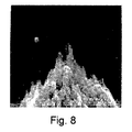
- the carbon polymer layer 4 continues to be etched as shown in FIGS. 6A and 6B, the carbon polymer layer 4 is almost removed and the target layer 2 begins to be etched. Finally, the target layer 2 originally having a flat surface has nano-sized surface features as shown in FIGS. 7A and 7B.
- the surface roughness of the micro structure are adjusted depending on the difference in etch rate between the micro structure and the carbon polymer layer 4.
- the etch rate is preferably controlled by adjusting at least one of plasma power, the O 2 content of the reactive gas with respect to the etch gas for etching the micro structure, or a plasma process pressure.
- FIG. 8 is an electron micrograph showing the structure of the target layer 2 of FIG. 7B having nano-sized surface features formed on the substrate 1, which is subjected to the above process.
- the method of forming a micro structure having nano-sized surface features as described above is suitable for formation of an electron emission source such as a field emission display. Furthermore, any other micro structure having nano-sized surface features can be manufactured easily by the method.
- a gate turn on voltage and a working voltage are reduced by about 20 V and 40 - 50 V, respectively, compared to a conventional FED having the same structure.
- a working voltage refers to a voltage at which emission current of 0.3mA is obtained at duty ratio of 1/90 and frequency of 60 Hz.
- the height and surface roughness of the micro tip can be adjusted by appropriately controlling an etch rate or etch speed between the micro tip and the carbon polymer layer according to plasma process conditions.
- the etch rate is adjusted by controlling at least of one of plasma power, the O 2 content of the reactive gas with respect to the etch gas for etching the micro structure, and a plasma process pressure.
- the present invention can easily give nano-sized surface features to the surface of a regularly structured micro structure.
- the method of forming a micro structure according to the present invention may be included in a process of forming another micro structure having a desired function.
- the present invention can also be applied to any structure other than FED, which requires the structure as described above.
Landscapes
- Engineering & Computer Science (AREA)
- Manufacturing & Machinery (AREA)
- Microelectronics & Electronic Packaging (AREA)
- Drying Of Semiconductors (AREA)
- ing And Chemical Polishing (AREA)
- Cold Cathode And The Manufacture (AREA)
- Micromachines (AREA)
Abstract
Description
Claims (9)
- A method of forming a micro structure having nano-sized surface features, the method comprising the steps of:forming a micro structure having predetermined size and shape on a substrate;coating a carbon polymer layer on the substrate including the micro structure to a predetermined thickness;performing a first etch on the carbon polymer layer by means of plasma etching using a reactive gas in which O2 gas for etching the carbon polymer layer and a gas for etching the micro structure are mixed and forming a mask layer by the residual carbon polymer layer on the surface of the micro structure; andperforming a second etch by means of plasma etching using the mixed reactive gas to remove the mask layer and etch the surface of the micro structure not covered by the mask layer so that the micro structure has nano-sized surface features.
- The method of claim 1, wherein the carbon polymer layer is formed of polyimide or photoresist.
- The method of claim 1 or 2, wherein the carbon polymer layer is etched using reactive ion etching (RIE).
- The method of claim 3, wherein the surface roughness are controlled by adjusting the difference in etch rate between the micro structure and the carbon polymer layer.
- The method of claim 4, wherein the etch rate is adjusted by at least one of plasma power, the O2 content of the reactive gas with respect to the etch gas for etching the micro structure and a plasma process pressure.
- The method of claim 3, wherein the micro structure is formed of one or a mixture of two or more selected among the group consisting of molybdenum (Mo), tungsten (W), silicon, and diamond, and the reactive gas is a mixture of O2 gas and fluorine-family gas.
- The method of claim 6, wherein the reactive gas comprises at least one of CF4/O2, SF6/O2, CHF3/O2, CF4/SF6/O2, CF4/CHF3/O2, and SF6/CHF3/O2.
- The method of claim 3, wherein the micro structure is formed of one or a mixture of two or more selected among the group consisting of molybdenum (Mo), tungsten (W), silicon, and diamond, and the reactive gas is a mixture of O2 gas and chlorine-family gas.
- The method of claim 8, wherein the reactive gas comprises at least one of Cl2/O2, CCl4/O2, and Cl2/CCl4/O2.
Applications Claiming Priority (2)
| Application Number | Priority Date | Filing Date | Title |
|---|---|---|---|
| KR10-2000-0000363A KR100480772B1 (en) | 2000-01-05 | 2000-01-05 | Forming method of micro structure with surface roughness of nano scale |
| KR2000000363 | 2000-01-05 |
Publications (3)
| Publication Number | Publication Date |
|---|---|
| EP1114791A2 true EP1114791A2 (en) | 2001-07-11 |
| EP1114791A3 EP1114791A3 (en) | 2002-07-24 |
| EP1114791B1 EP1114791B1 (en) | 2007-05-02 |
Family
ID=19636546
Family Applications (1)
| Application Number | Title | Priority Date | Filing Date |
|---|---|---|---|
| EP01300023A Expired - Lifetime EP1114791B1 (en) | 2000-01-05 | 2001-01-03 | Method of forming structure having surface roughness due to nano-sized surface features |
Country Status (5)
| Country | Link |
|---|---|
| US (1) | US6468916B2 (en) |
| EP (1) | EP1114791B1 (en) |
| JP (1) | JP2001262376A (en) |
| KR (1) | KR100480772B1 (en) |
| DE (1) | DE60128165T2 (en) |
Cited By (3)
| Publication number | Priority date | Publication date | Assignee | Title |
|---|---|---|---|---|
| KR100480772B1 (en) * | 2000-01-05 | 2005-04-06 | 삼성에스디아이 주식회사 | Forming method of micro structure with surface roughness of nano scale |
| DE102005037139A1 (en) * | 2005-08-06 | 2007-02-08 | Technische Universität Ilmenau | Method for connecting microcomponents with nanostructured silicon surfaces and method for their production |
| CN1325401C (en) * | 2002-03-29 | 2007-07-11 | Otv股份有限公司 | Circular plants for the biological treatment of wastewater |
Families Citing this family (16)
| Publication number | Priority date | Publication date | Assignee | Title |
|---|---|---|---|---|
| JP2002280354A (en) * | 2001-03-19 | 2002-09-27 | Osaka Prefecture | Method and apparatus for etching carbon thin film |
| US6767825B1 (en) * | 2003-02-03 | 2004-07-27 | United Microelectronics Corporation | Etching process for forming damascene structure of the semiconductor |
| US7052618B2 (en) * | 2004-01-28 | 2006-05-30 | Agilent Technologies, Inc. | Nanostructures and methods of making the same |
| GR1006890B (en) * | 2005-09-16 | 2010-07-19 | Ευαγγελος Γογγολιδης | Method for the fabrication of high surface area ratio and high aspect ratio surfaces on substrates |
| EP2170764A4 (en) * | 2007-06-21 | 2011-06-22 | 3M Innovative Properties Co | Methods of making hierarchical articles |
| FI20070953L (en) * | 2007-12-10 | 2009-06-11 | Beneq Oy | Method and device for structuring a surface |
| FI123691B (en) | 2007-12-10 | 2013-09-30 | Beneq Oy | A method for producing a highly hydrophobic surface |
| KR101100859B1 (en) * | 2010-03-19 | 2012-01-02 | 포항공과대학교 산학협력단 | Multi-scale surface processing method and solid substrate having a multi-scale surface produced by the method |
| CN102180438A (en) * | 2011-03-28 | 2011-09-14 | 中国科学院光电技术研究所 | Fabrication method of a tunable triangular metal nanoparticle array structure |
| TWI601250B (en) * | 2011-07-22 | 2017-10-01 | 先進封裝技術私人有限公司 | Semiconductor structure for manufacturing semiconductor package component and method of fabricating the same |
| CN103924241B (en) * | 2014-04-14 | 2017-01-18 | 北京工业大学 | Method for on-scale preparation of tungsten with micro-nano structure on surface with low surface stress |
| KR102567715B1 (en) * | 2016-04-29 | 2023-08-17 | 삼성디스플레이 주식회사 | Transistor array panel and manufacturing method thereof |
| CN109972115B (en) * | 2017-12-28 | 2021-01-19 | 深圳先进技术研究院 | Hard alloy cutter with micro-nano diamond coating and preparation method thereof |
| US11192782B1 (en) * | 2020-09-01 | 2021-12-07 | Aac Acoustic Technologies (Shenzhen) Co., Ltd. | Method for preparing silicon wafer with rough surface and silicon wafer |
| US11305988B2 (en) * | 2020-09-01 | 2022-04-19 | Aac Acoustic Technologies (Shenzhen) Co., Ltd. | Method for preparing silicon wafer with rough surface and silicon wafer |
| CN120413416A (en) * | 2025-05-08 | 2025-08-01 | 慕德微纳(杭州)科技有限公司 | A wafer surface roughness optimization processing method |
Family Cites Families (10)
| Publication number | Priority date | Publication date | Assignee | Title |
|---|---|---|---|---|
| EP0117258B1 (en) * | 1983-02-23 | 1987-05-20 | Ibm Deutschland Gmbh | Process for the production of metallic layers adhering to plastic supports |
| JPS6218714A (en) * | 1985-07-18 | 1987-01-27 | Nippon Telegr & Teleph Corp <Ntt> | Forming method for alignment mark |
| JPH04216662A (en) * | 1990-12-17 | 1992-08-06 | Mitsubishi Electric Corp | Manufacture of semiconductor storage device |
| US5564959A (en) * | 1993-09-08 | 1996-10-15 | Silicon Video Corporation | Use of charged-particle tracks in fabricating gated electron-emitting devices |
| US5753420A (en) * | 1995-09-18 | 1998-05-19 | Texas Instruments Incorporated | Rough dielectric film by etchback of residue |
| US5637189A (en) * | 1996-06-25 | 1997-06-10 | Xerox Corporation | Dry etch process control using electrically biased stop junctions |
| US6193870B1 (en) * | 1997-05-01 | 2001-02-27 | The Regents Of The University Of California | Use of a hard mask for formation of gate and dielectric via nanofilament field emission devices |
| KR100480771B1 (en) * | 2000-01-05 | 2005-04-06 | 삼성에스디아이 주식회사 | Field emission device and the fabrication method thereof |
| KR100480772B1 (en) * | 2000-01-05 | 2005-04-06 | 삼성에스디아이 주식회사 | Forming method of micro structure with surface roughness of nano scale |
| KR100464314B1 (en) * | 2000-01-05 | 2004-12-31 | 삼성에스디아이 주식회사 | Field emission device and the fabrication method thereof |
-
2000
- 2000-01-05 KR KR10-2000-0000363A patent/KR100480772B1/en not_active Expired - Fee Related
-
2001
- 2001-01-03 EP EP01300023A patent/EP1114791B1/en not_active Expired - Lifetime
- 2001-01-03 DE DE60128165T patent/DE60128165T2/en not_active Expired - Lifetime
- 2001-01-05 JP JP2001000347A patent/JP2001262376A/en active Pending
- 2001-01-05 US US09/754,274 patent/US6468916B2/en not_active Expired - Fee Related
Cited By (4)
| Publication number | Priority date | Publication date | Assignee | Title |
|---|---|---|---|---|
| KR100480772B1 (en) * | 2000-01-05 | 2005-04-06 | 삼성에스디아이 주식회사 | Forming method of micro structure with surface roughness of nano scale |
| CN1325401C (en) * | 2002-03-29 | 2007-07-11 | Otv股份有限公司 | Circular plants for the biological treatment of wastewater |
| DE102005037139A1 (en) * | 2005-08-06 | 2007-02-08 | Technische Universität Ilmenau | Method for connecting microcomponents with nanostructured silicon surfaces and method for their production |
| WO2007017458A1 (en) * | 2005-08-06 | 2007-02-15 | Technische Universität Ilmenau | Microcomponent with nanostructured silicon surface, method for producing it, and connection arrangement comprising such microcomponents |
Also Published As
| Publication number | Publication date |
|---|---|
| KR100480772B1 (en) | 2005-04-06 |
| EP1114791A3 (en) | 2002-07-24 |
| KR20010068443A (en) | 2001-07-23 |
| US6468916B2 (en) | 2002-10-22 |
| EP1114791B1 (en) | 2007-05-02 |
| DE60128165D1 (en) | 2007-06-14 |
| JP2001262376A (en) | 2001-09-26 |
| DE60128165T2 (en) | 2007-12-27 |
| US20010006851A1 (en) | 2001-07-05 |
Similar Documents
| Publication | Publication Date | Title |
|---|---|---|
| EP1114791B1 (en) | Method of forming structure having surface roughness due to nano-sized surface features | |
| US6406979B2 (en) | Method for sectioning a substrate wafer into a plurality of substrate chips | |
| US5160407A (en) | Low pressure anisotropic etch process for tantalum silicide or titanium silicide layer formed over polysilicon layer deposited on silicon oxide layer on semiconductor wafer | |
| EP0379298B1 (en) | Method of forming an electrode for an electron emitting device | |
| US5302238A (en) | Plasma dry etch to produce atomically sharp asperities useful as cold cathodes | |
| CN1294542A (en) | Diamond cutting tool | |
| KR20020061480A (en) | Fine pattern forming method, semiconductor device manufacturing method, and semiconductor device | |
| WO2008005630A2 (en) | Methods for minimizing mask undercuts and notches for plasma processing system | |
| JP2002075171A (en) | Method of manufacturing electron-emitting device and electronic device | |
| EP1638137A1 (en) | Electron beam microprocessing method | |
| KR100480771B1 (en) | Field emission device and the fabrication method thereof | |
| US6916748B2 (en) | Method of forming emitter tips on a field emission display | |
| KR0166205B1 (en) | Polyside gate formation method of semiconductor device | |
| US6702637B2 (en) | Method of forming a small gap and its application to the fabrication of a lateral FED | |
| US20050263483A1 (en) | Modifying the viscosity of etchants | |
| US7091081B2 (en) | Method for patterning a semiconductor region | |
| KR100208474B1 (en) | Field emission micro-tip and its manufacturing method | |
| JP2695919B2 (en) | Wiring pattern forming method | |
| KR0163086B1 (en) | Method of forming a contact hole in a semiconductor device | |
| KR20010072923A (en) | Emitter, emitter fabricating method, and cold electron emitting device fabricating method | |
| CN1731564A (en) | Method for etching holes with different aspect ratios | |
| JPH05347279A (en) | Plasma etching method and apparatus | |
| JPH05217959A (en) | Method for manufacturing semiconductor device | |
| CN117476455A (en) | Method for forming conductive layer of semiconductor element | |
| JPH07135198A (en) | Etching |
Legal Events
| Date | Code | Title | Description |
|---|---|---|---|
| PUAI | Public reference made under article 153(3) epc to a published international application that has entered the european phase |
Free format text: ORIGINAL CODE: 0009012 |
|
| AK | Designated contracting states |
Kind code of ref document: A2 Designated state(s): AT BE CH CY DE DK ES FI FR GB GR IE IT LI LU MC NL PT SE TR |
|
| AX | Request for extension of the european patent |
Free format text: AL;LT;LV;MK;RO;SI |
|
| PUAL | Search report despatched |
Free format text: ORIGINAL CODE: 0009013 |
|
| AK | Designated contracting states |
Kind code of ref document: A3 Designated state(s): AT BE CH CY DE DK ES FI FR GB GR IE IT LI LU MC NL PT SE TR |
|
| AX | Request for extension of the european patent |
Free format text: AL;LT;LV;MK;RO;SI |
|
| 17P | Request for examination filed |
Effective date: 20021030 |
|
| AKX | Designation fees paid |
Designated state(s): DE FR GB |
|
| GRAP | Despatch of communication of intention to grant a patent |
Free format text: ORIGINAL CODE: EPIDOSNIGR1 |
|
| GRAS | Grant fee paid |
Free format text: ORIGINAL CODE: EPIDOSNIGR3 |
|
| GRAA | (expected) grant |
Free format text: ORIGINAL CODE: 0009210 |
|
| AK | Designated contracting states |
Kind code of ref document: B1 Designated state(s): DE FR GB |
|
| REG | Reference to a national code |
Ref country code: GB Ref legal event code: FG4D |
|
| REF | Corresponds to: |
Ref document number: 60128165 Country of ref document: DE Date of ref document: 20070614 Kind code of ref document: P |
|
| ET | Fr: translation filed | ||
| PLBE | No opposition filed within time limit |
Free format text: ORIGINAL CODE: 0009261 |
|
| STAA | Information on the status of an ep patent application or granted ep patent |
Free format text: STATUS: NO OPPOSITION FILED WITHIN TIME LIMIT |
|
| 26N | No opposition filed |
Effective date: 20080205 |
|
| PGFP | Annual fee paid to national office [announced via postgrant information from national office to epo] |
Ref country code: GB Payment date: 20101229 Year of fee payment: 11 |
|
| PGFP | Annual fee paid to national office [announced via postgrant information from national office to epo] |
Ref country code: DE Payment date: 20101230 Year of fee payment: 11 Ref country code: FR Payment date: 20110128 Year of fee payment: 11 |
|
| GBPC | Gb: european patent ceased through non-payment of renewal fee |
Effective date: 20120103 |
|
| REG | Reference to a national code |
Ref country code: FR Ref legal event code: ST Effective date: 20120928 |
|
| PG25 | Lapsed in a contracting state [announced via postgrant information from national office to epo] |
Ref country code: GB Free format text: LAPSE BECAUSE OF NON-PAYMENT OF DUE FEES Effective date: 20120103 Ref country code: DE Free format text: LAPSE BECAUSE OF NON-PAYMENT OF DUE FEES Effective date: 20120801 |
|
| REG | Reference to a national code |
Ref country code: DE Ref legal event code: R119 Ref document number: 60128165 Country of ref document: DE Effective date: 20120801 |
|
| PG25 | Lapsed in a contracting state [announced via postgrant information from national office to epo] |
Ref country code: FR Free format text: LAPSE BECAUSE OF NON-PAYMENT OF DUE FEES Effective date: 20120131 |