EP1114551B1 - Improved apparatus for scanning documents such as photographs using a contact image sensor - Google Patents
Improved apparatus for scanning documents such as photographs using a contact image sensor Download PDFInfo
- Publication number
- EP1114551B1 EP1114551B1 EP99937255A EP99937255A EP1114551B1 EP 1114551 B1 EP1114551 B1 EP 1114551B1 EP 99937255 A EP99937255 A EP 99937255A EP 99937255 A EP99937255 A EP 99937255A EP 1114551 B1 EP1114551 B1 EP 1114551B1
- Authority
- EP
- European Patent Office
- Prior art keywords
- document
- scanner window
- stick material
- scanning
- documents according
- Prior art date
- Legal status (The legal status is an assumption and is not a legal conclusion. Google has not performed a legal analysis and makes no representation as to the accuracy of the status listed.)
- Expired - Lifetime
Links
- 239000000463 material Substances 0.000 claims abstract description 91
- 230000003068 static effect Effects 0.000 claims abstract description 13
- 230000005611 electricity Effects 0.000 claims abstract description 8
- 239000004699 Ultra-high molecular weight polyethylene Substances 0.000 claims description 14
- 229920000785 ultra high molecular weight polyethylene Polymers 0.000 claims description 14
- 239000004677 Nylon Substances 0.000 claims description 11
- 229920001778 nylon Polymers 0.000 claims description 11
- 229920001296 polysiloxane Polymers 0.000 claims description 11
- 229920002313 fluoropolymer Polymers 0.000 claims description 10
- 239000004811 fluoropolymer Substances 0.000 claims description 10
- OKTJSMMVPCPJKN-UHFFFAOYSA-N Carbon Chemical compound [C] OKTJSMMVPCPJKN-UHFFFAOYSA-N 0.000 claims description 8
- 229920000049 Carbon (fiber) Polymers 0.000 claims description 8
- 239000004917 carbon fiber Substances 0.000 claims description 8
- 239000000839 emulsion Substances 0.000 claims description 4
- 230000006872 improvement Effects 0.000 claims description 4
- 230000003678 scratch resistant effect Effects 0.000 claims description 3
- QTBSBXVTEAMEQO-UHFFFAOYSA-M Acetate Chemical compound CC([O-])=O QTBSBXVTEAMEQO-UHFFFAOYSA-M 0.000 claims 6
- 239000011347 resin Substances 0.000 claims 6
- 229920005989 resin Polymers 0.000 claims 6
- 230000004075 alteration Effects 0.000 claims 2
- 230000006978 adaptation Effects 0.000 claims 1
- 230000009467 reduction Effects 0.000 abstract description 2
- 238000013461 design Methods 0.000 description 8
- 238000005286 illumination Methods 0.000 description 8
- 230000004048 modification Effects 0.000 description 6
- 238000012986 modification Methods 0.000 description 6
- DHKHKXVYLBGOIT-UHFFFAOYSA-N 1,1-Diethoxyethane Chemical compound CCOC(C)OCC DHKHKXVYLBGOIT-UHFFFAOYSA-N 0.000 description 5
- 239000011354 acetal resin Substances 0.000 description 5
- 230000003287 optical effect Effects 0.000 description 5
- 229920006324 polyoxymethylene Polymers 0.000 description 5
- 229920004943 Delrin® Polymers 0.000 description 4
- 229920006362 Teflon® Polymers 0.000 description 4
- -1 polytetrafluorethylene Polymers 0.000 description 4
- 229920001343 polytetrafluoroethylene Polymers 0.000 description 4
- 230000002829 reductive effect Effects 0.000 description 4
- 239000012780 transparent material Substances 0.000 description 4
- 229920002574 CR-39 Polymers 0.000 description 3
- NIXOWILDQLNWCW-UHFFFAOYSA-N acrylic acid group Chemical group C(C=C)(=O)O NIXOWILDQLNWCW-UHFFFAOYSA-N 0.000 description 3
- 238000005516 engineering process Methods 0.000 description 3
- 239000011521 glass Substances 0.000 description 3
- 238000003384 imaging method Methods 0.000 description 3
- 238000004519 manufacturing process Methods 0.000 description 3
- 229920003023 plastic Polymers 0.000 description 3
- 239000004033 plastic Substances 0.000 description 3
- 229920000515 polycarbonate Polymers 0.000 description 3
- 239000004417 polycarbonate Substances 0.000 description 3
- 239000004809 Teflon Substances 0.000 description 2
- 238000013037 co-molding Methods 0.000 description 2
- 150000001875 compounds Chemical class 0.000 description 2
- 238000000151 deposition Methods 0.000 description 2
- 239000000835 fiber Substances 0.000 description 2
- 230000007246 mechanism Effects 0.000 description 2
- 239000000758 substrate Substances 0.000 description 2
- NNWNNQTUZYVQRK-UHFFFAOYSA-N 5-bromo-1h-pyrrolo[2,3-c]pyridine-2-carboxylic acid Chemical compound BrC1=NC=C2NC(C(=O)O)=CC2=C1 NNWNNQTUZYVQRK-UHFFFAOYSA-N 0.000 description 1
- XUIMIQQOPSSXEZ-UHFFFAOYSA-N Silicon Chemical compound [Si] XUIMIQQOPSSXEZ-UHFFFAOYSA-N 0.000 description 1
- 239000000853 adhesive Substances 0.000 description 1
- 230000001070 adhesive effect Effects 0.000 description 1
- 238000003491 array Methods 0.000 description 1
- 239000011230 binding agent Substances 0.000 description 1
- 230000005540 biological transmission Effects 0.000 description 1
- 229910052799 carbon Inorganic materials 0.000 description 1
- 230000008859 change Effects 0.000 description 1
- 238000000701 chemical imaging Methods 0.000 description 1
- 238000006243 chemical reaction Methods 0.000 description 1
- 239000011248 coating agent Substances 0.000 description 1
- 238000000576 coating method Methods 0.000 description 1
- 230000003247 decreasing effect Effects 0.000 description 1
- 230000008021 deposition Effects 0.000 description 1
- 229920006351 engineering plastic Polymers 0.000 description 1
- 230000001939 inductive effect Effects 0.000 description 1
- 238000003780 insertion Methods 0.000 description 1
- 230000037431 insertion Effects 0.000 description 1
- 230000003993 interaction Effects 0.000 description 1
- 230000002452 interceptive effect Effects 0.000 description 1
- VNWKTOKETHGBQD-UHFFFAOYSA-N methane Chemical compound C VNWKTOKETHGBQD-UHFFFAOYSA-N 0.000 description 1
- 238000000034 method Methods 0.000 description 1
- 238000005065 mining Methods 0.000 description 1
- 239000000178 monomer Substances 0.000 description 1
- 230000036961 partial effect Effects 0.000 description 1
- 239000002245 particle Substances 0.000 description 1
- 229920000642 polymer Polymers 0.000 description 1
- 230000001681 protective effect Effects 0.000 description 1
- 238000006748 scratching Methods 0.000 description 1
- 230000002393 scratching effect Effects 0.000 description 1
- 229910052710 silicon Inorganic materials 0.000 description 1
- 239000010703 silicon Substances 0.000 description 1
- BFKJFAAPBSQJPD-UHFFFAOYSA-N tetrafluoroethene Chemical compound FC(F)=C(F)F BFKJFAAPBSQJPD-UHFFFAOYSA-N 0.000 description 1
- 229920001187 thermosetting polymer Polymers 0.000 description 1
- XLYOFNOQVPJJNP-UHFFFAOYSA-N water Substances O XLYOFNOQVPJJNP-UHFFFAOYSA-N 0.000 description 1
Images

Classifications
-
- H—ELECTRICITY
- H04—ELECTRIC COMMUNICATION TECHNIQUE
- H04N—PICTORIAL COMMUNICATION, e.g. TELEVISION
- H04N1/00—Scanning, transmission or reproduction of documents or the like, e.g. facsimile transmission; Details thereof
- H04N1/024—Details of scanning heads ; Means for illuminating the original
- H04N1/028—Details of scanning heads ; Means for illuminating the original for picture information pick-up
- H04N1/03—Details of scanning heads ; Means for illuminating the original for picture information pick-up with photodetectors arranged in a substantially linear array
- H04N1/031—Details of scanning heads ; Means for illuminating the original for picture information pick-up with photodetectors arranged in a substantially linear array the photodetectors having a one-to-one and optically positive correspondence with the scanned picture elements, e.g. linear contact sensors
- H04N1/0311—Details of scanning heads ; Means for illuminating the original for picture information pick-up with photodetectors arranged in a substantially linear array the photodetectors having a one-to-one and optically positive correspondence with the scanned picture elements, e.g. linear contact sensors using an array of elements to project the scanned image elements onto the photodetectors
- H04N1/0312—Details of scanning heads ; Means for illuminating the original for picture information pick-up with photodetectors arranged in a substantially linear array the photodetectors having a one-to-one and optically positive correspondence with the scanned picture elements, e.g. linear contact sensors using an array of elements to project the scanned image elements onto the photodetectors using an array of optical fibres or rod-lenses
-
- H—ELECTRICITY
- H04—ELECTRIC COMMUNICATION TECHNIQUE
- H04N—PICTORIAL COMMUNICATION, e.g. TELEVISION
- H04N1/00—Scanning, transmission or reproduction of documents or the like, e.g. facsimile transmission; Details thereof
- H04N1/024—Details of scanning heads ; Means for illuminating the original
- H04N1/028—Details of scanning heads ; Means for illuminating the original for picture information pick-up
- H04N1/03—Details of scanning heads ; Means for illuminating the original for picture information pick-up with photodetectors arranged in a substantially linear array
- H04N1/031—Details of scanning heads ; Means for illuminating the original for picture information pick-up with photodetectors arranged in a substantially linear array the photodetectors having a one-to-one and optically positive correspondence with the scanned picture elements, e.g. linear contact sensors
- H04N1/0311—Details of scanning heads ; Means for illuminating the original for picture information pick-up with photodetectors arranged in a substantially linear array the photodetectors having a one-to-one and optically positive correspondence with the scanned picture elements, e.g. linear contact sensors using an array of elements to project the scanned image elements onto the photodetectors
-
- H—ELECTRICITY
- H04—ELECTRIC COMMUNICATION TECHNIQUE
- H04N—PICTORIAL COMMUNICATION, e.g. TELEVISION
- H04N1/00—Scanning, transmission or reproduction of documents or the like, e.g. facsimile transmission; Details thereof
- H04N1/024—Details of scanning heads ; Means for illuminating the original
- H04N1/028—Details of scanning heads ; Means for illuminating the original for picture information pick-up
- H04N1/03—Details of scanning heads ; Means for illuminating the original for picture information pick-up with photodetectors arranged in a substantially linear array
- H04N1/031—Details of scanning heads ; Means for illuminating the original for picture information pick-up with photodetectors arranged in a substantially linear array the photodetectors having a one-to-one and optically positive correspondence with the scanned picture elements, e.g. linear contact sensors
- H04N1/0315—Details of scanning heads ; Means for illuminating the original for picture information pick-up with photodetectors arranged in a substantially linear array the photodetectors having a one-to-one and optically positive correspondence with the scanned picture elements, e.g. linear contact sensors using photodetectors and illumination means mounted on separate supports or substrates or mounted in different planes
-
- H—ELECTRICITY
- H04—ELECTRIC COMMUNICATION TECHNIQUE
- H04N—PICTORIAL COMMUNICATION, e.g. TELEVISION
- H04N1/00—Scanning, transmission or reproduction of documents or the like, e.g. facsimile transmission; Details thereof
- H04N1/04—Scanning arrangements, i.e. arrangements for the displacement of active reading or reproducing elements relative to the original or reproducing medium, or vice versa
- H04N1/12—Scanning arrangements, i.e. arrangements for the displacement of active reading or reproducing elements relative to the original or reproducing medium, or vice versa using the sheet-feed movement or the medium-advance or the drum-rotation movement as the slow scanning component, e.g. arrangements for the main-scanning
- H04N1/121—Feeding arrangements
-
- H—ELECTRICITY
- H04—ELECTRIC COMMUNICATION TECHNIQUE
- H04N—PICTORIAL COMMUNICATION, e.g. TELEVISION
- H04N2201/00—Indexing scheme relating to scanning, transmission or reproduction of documents or the like, and to details thereof
- H04N2201/024—Indexing scheme relating to scanning, transmission or reproduction of documents or the like, and to details thereof deleted
- H04N2201/02495—Constructional details not otherwise provided for, e.g. for ease of assembly, allowing access to the scanning elements, integrated reinforcing members
-
- H—ELECTRICITY
- H04—ELECTRIC COMMUNICATION TECHNIQUE
- H04N—PICTORIAL COMMUNICATION, e.g. TELEVISION
- H04N2201/00—Indexing scheme relating to scanning, transmission or reproduction of documents or the like, and to details thereof
- H04N2201/024—Indexing scheme relating to scanning, transmission or reproduction of documents or the like, and to details thereof deleted
- H04N2201/028—Indexing scheme relating to scanning, transmission or reproduction of documents or the like, and to details thereof deleted for picture information pick-up
- H04N2201/03—Indexing scheme relating to scanning, transmission or reproduction of documents or the like, and to details thereof deleted for picture information pick-up deleted
- H04N2201/031—Indexing scheme relating to scanning, transmission or reproduction of documents or the like, and to details thereof deleted for picture information pick-up deleted deleted
- H04N2201/03104—Integral pick-up heads, i.e. self-contained heads whose basic elements are a light source, a lens and a photodetector supported by a single-piece frame
- H04N2201/03108—Components of integral heads
- H04N2201/03133—Window, i.e. a transparent member mounted in the frame
-
- H—ELECTRICITY
- H04—ELECTRIC COMMUNICATION TECHNIQUE
- H04N—PICTORIAL COMMUNICATION, e.g. TELEVISION
- H04N2201/00—Indexing scheme relating to scanning, transmission or reproduction of documents or the like, and to details thereof
- H04N2201/024—Indexing scheme relating to scanning, transmission or reproduction of documents or the like, and to details thereof deleted
- H04N2201/028—Indexing scheme relating to scanning, transmission or reproduction of documents or the like, and to details thereof deleted for picture information pick-up
- H04N2201/03—Indexing scheme relating to scanning, transmission or reproduction of documents or the like, and to details thereof deleted for picture information pick-up deleted
- H04N2201/031—Indexing scheme relating to scanning, transmission or reproduction of documents or the like, and to details thereof deleted for picture information pick-up deleted deleted
- H04N2201/03104—Integral pick-up heads, i.e. self-contained heads whose basic elements are a light source, a lens and a photodetector supported by a single-piece frame
- H04N2201/0315—Details of integral heads not otherwise provided for
- H04N2201/0317—Shape
-
- H—ELECTRICITY
- H04—ELECTRIC COMMUNICATION TECHNIQUE
- H04N—PICTORIAL COMMUNICATION, e.g. TELEVISION
- H04N2201/00—Indexing scheme relating to scanning, transmission or reproduction of documents or the like, and to details thereof
- H04N2201/024—Indexing scheme relating to scanning, transmission or reproduction of documents or the like, and to details thereof deleted
- H04N2201/028—Indexing scheme relating to scanning, transmission or reproduction of documents or the like, and to details thereof deleted for picture information pick-up
- H04N2201/03—Indexing scheme relating to scanning, transmission or reproduction of documents or the like, and to details thereof deleted for picture information pick-up deleted
- H04N2201/031—Indexing scheme relating to scanning, transmission or reproduction of documents or the like, and to details thereof deleted for picture information pick-up deleted deleted
- H04N2201/03104—Integral pick-up heads, i.e. self-contained heads whose basic elements are a light source, a lens and a photodetector supported by a single-piece frame
- H04N2201/0315—Details of integral heads not otherwise provided for
- H04N2201/03183—Material
Definitions
- the invention relates to an apparatus for scanning a document according to the preamble of claim 1, and in particular the design and implementation of contact image sensors in scanning devices to allow for the scanning of photographic paper, specifically by reducing the sliding friction of the scanner window surface.
- An apparatus of the initially-mentioned type is known, e.g., from EP-A-0 603 903 .
- High-quality "scanning" of physical documents such as business documents into digital form is routinely accomplished in commercially available devices such as computer-attached document scanners and facsimile machines.
- Document scanners are used to convert images to digital form for inclusion in computer files. Facsimile machines transmit the digital information over telephone lines to other facsimile machines, which then recreate the original document.
- the conversion of the document from physical to digital form is accomplished in an image sensor unit.
- the image sensor is a charge coupled device (CCD) or a silicon image sensor. Illumination is provided by an illuminating device, while the optics for focusing from the surface of the document to the image sensor is provided with mirror(s) and lenses.
- a CIS typically incorporates illumination, focusing optics in the form of a narrow depth of focus lens array, and sensor arrays in one package.
- the narrow depth of focus lens array optics usually is a gradient index fiber optic array.
- the compact unit is often sealed, with illumination and document scanning occurring through a single "scanner window.” Scanning devices are constructed so that the CIS image sensor unit scans the width of the document, which is placed at the focus of the unit, while the length of the document is scanned by inducing relative motion between the document and the sensor unit.
- the advantages of a CIS device over traditional sensor technology include: ease of manufacturing, reduced component count, fewer moving parts, reduced cost, integrated optics, and environmentally controlled optical path.
- the relative motion between the document and the image sensor unit is obtained through one of two configurations.
- the first typically is used by "flat bed” scanners and copiers.
- the CIS usually does not have a physical scanner window, and the document is placed on top of a sheet of transparent material, usually a glass platen, with an image scanner located below and focused through the transparent material.
- the CIS image scanner unit is forced to move the length of the document through a drive mechanism while the document remains stationary. This configuration is not the main area of application of the present invention.
- a second configuration is suitable for use in facsimile machines, hand-held scanners and sheet-fed scanners, and is the main area of application of the present invention.
- the CIS unit is arranged so that the focus of the sensor-lens system is coincident with the outer surface of a window that is fixed to the CIS.
- the document must be placed essentially in contact with the scanner window for the document to be in focus, and such a short (essentially zero) document-to-sensor window distance must be maintained while scanning. Because of the utility of this arrangement, sealed contact image sensors are common in facsimile machines and other inexpensive document scanners, and devices that use them must be configured so that the document to be scanned slides across the scanner window.
- the contact image sensor arrangement has several advantages. Image sensor units are relatively durable and low cost, resulting in the near ubiquity of facsimile machines, and in the low cost of black and white or gray scale document scanners. Contact image sensors usually have a very small depth of focus however, on the order of two tenths of a millimeter, and so reliable scanning is accomplished only with a document in good contact with the scanner window. The relatively narrow depth of field of contact image sensors results in design problems that are not present in image sensors where the depth of field can be varied. The recent introduction of color contact image sensors provides yet another design problem: color scanners are used for photographs as well as printed documents, and thus the contact image sensor must be compatible with photographic media. Contact is not a problem with many types of common document material, such as smooth paper. However, scanners based on contact image sensors technology suffer from the inability to scan materials that cannot pass smoothly by the scanner unit. Specifically, photographic documents cannot reliably be used with contact image sensors. This inability manifests itself in the following ways:
- the reason for the problems encountered with CIS scanning of photographs, as enumerated above, has to do with the interaction between soft photographic emulsions and the scanner window surface.
- a modification to the design of a traditional scanner window is proposed. Specifically, the modification includes reducing the amount of friction between the document and the outer surface of the scanner window, thus enabling contact image sensors to work for photographs with the same reliability and ease with which they work with paper and other document materials.
- One object of the present invention is to allow CIS scanning to be useful in scanning documents that have the propensity to stick to the scanner window.
- Another object of the invention is to reduce the incidence of document jamming that occurs during CIS scanning of photographic or similar documents.
- Another object is to reduce the incidence of spotting that occurs during the CIS scanning of photographic or similar documents.
- Another object is to reduce the incidence of scratching of documents that occurs during the CIS scanning of photographic or similar documents.
- the foregoing and other objects and advantages are attained by including a scanner window which has a low coefficient of sliding friction with the document.
- the scanner window is recessed in areas away from the focal area of the CIS unit to allow for the addition of non-slip material in those areas, while not interfering with the focus of the CIS optics.
- the scanner window is recessed in areas away from the focal area of the CIS unit and includes non-slip material in those areas.
- the scanner window is coated with a combination of light-transmitting and non-stick materials to allow for the smooth passage of the document over the CIS unit, and the transmission of the document image to the sensor array, the optics adapted to focus through the coating.
- the non-focal area portion of the scanner window is coated with a layer of non-stick material that is less than the focal depth of the scanner optics.
- Fig. 1 shows a perspective view of a typical contact image sensor (CIS) 101 traversing a document. While a CIS such as CIS 101 shown in Fig. 1 is prior art, and hence is so labeled, a CIS with the friction reducing modifications described herein and a CIS with the reduced friction elements described herein are not prior art.
- CIS 101 is positioned for scanning a document 103 by placing the transparent scanner window 105 substantially in contact with document 103 and producing relative motion between CIS 101 and document 103.
- scanner window 105 being substantially in contact with document 103 is meant that the distance between scanner window 105 and document 103 is very small so that the document remains in focus even given the narrow depth of field of the optics in CIS 101 .
- Typical CIS 101 components are compact, and document 103 is scanned in a direction perpendicular to the CIS length direction. Relative motion may occur by either moving the CIS over a fixed document, or by moving the document over a fixed CIS.
- necessary electrical connections for the operation of CIS 101 include a power supply 113 , and electronics 109 which convert the CIS output 107 to a useful output 111 .
- Elements 113 and 109 are standard as would be used in CIS scanners, including prior art CIS scanners and the CIS scanner of the invention.
- Fig. 2 shows a schematic cross-sectional side view of a typical CIS 101 , which is shown as section A-A in Fig. 1.
- the size and placement of the components in cross sectional view are approximately the same at any location down the length of the CIS.
- CIS 101 is shown in Fig. 2 in the proper position for scanning document 103.
- the CIS components are contained within an outer housing or cover 221 and transparent scanner window 105 .
- Scanner window 105 has an outer surface 237 facing document 103 during scanning, and a back surface 239 facing sensor array 229 .
- the components that are important in scanning are a light source 223 , focusing optics 225 , and a sensor array 229 .
- Scanner window 105 , optics 225 , sensor array 229 and light source 223 are all approximately the same length in a typical CIS.
- Sensor array 229 is part of a substrate 231 which contains electronics for controlling data flow from the output of sensor array 229 , producing CIS output 107 , shown in Fig. 1.
- Light source 223 includes a light producing unit, such as an incandescent light or a set of light emitting diodes, with or without a light pipe, that produces light that is projected along the length of CIS 101 and towards scanner window 105 . It is important that light source 223 illuminates at least part of document 103 with enough reflected light for sensor array 229 to produce a useful signal.
- Focusing optics 225 which can consist of a combination of lenses and mirrors or, as is typical in a CIS, a narrow depth of focus lens array such as a gradient index array (also called a self-focussing lens array, e.g.
- focusing optics 225 have a very narrow depth of field, typically less than one millimeter, and focussing optics 225 are adapted to focus an area (called the focal area 227 herein) on the scanner window outer surface 237 .
- focal area 227 is typically approximately one millimeter wide and has a length determined by the design of focusing optics.
- focal area edge rays 235 The trace of the edge of focal area optical rays from focal area 227 to sensor array 229 are shown as focal area edge rays 235 .
- the area of scanner window 105 that is not in focal area 227 is termed the non-focal area herein with reference numeral 233 .
- each point on scanner window outer surface 237 is in either focal area 227 or non-focal area 233 .
- components 231, 223, 229 , and 225 are not shown for the sake of simplicity.
- Fig. 3 shows a top view of document 103 with projections of scanner window 105 , focal area 227 and non-focal area 233 .
- the scanned area of document 103 is that area traced out by focal area 227 during the relative motion of the CIS and document 103 .
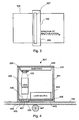
- Fig. 4 is a schematic side view of one embodiment of a contact image sensor 401 which includes features according to the present invention.
- the CIS includes an integral housing 441 that includes a housing scanning surface 443 substantially in contact with document 103 , up to but not including the focal area 427 leaving an opening in the front ( i.e., document) side of integral housing unit 441, 433 is the non-focal area.
- Integral housing 441 is made of a combination of non-stick and static dissipative materials in a plastic binder base material. Any material that reduces the friction with the document during scanning will do for the non-stick material, and preferably, the non-stick material has a substantially lower coefficient of friction with the document than does the scanner window. Many non-stick materials may be used.
- one can use one or more of a fluoropolymer e.g ., the polytetrafluorethylene TEFLON® from E.I. du Pont de Nemours and Company, Wilmington, Delaware
- silicone e.g ., silicone
- UHMW-PE ultra high molecular weight polyethylene
- Static dissipative materials to use include adding carbon fibers or carbon powder.
- Many materials are suitable for use as the base material, including polycarbonate, nylon, and an acetal resin (e.g., DELRIN® from E.I. du Pont de Nemours and Company, Wilmington, Delaware). Note nylon and the acetal resin already have a low coefficient of friction.
- Integral housing 441 is formed with an integral housing back cover 445 as a separate piece to allow for easy mounting of the CIS components.
- Scanner window 405 is located interior to and against the front (document) side of integral housing unit 441 , and thus has a protruding part 449 that fits in the opening of the front side of housing unit 441 .
- a portion of protruding part 449 is flush with housing surface 443 , contains the focal area 427 and non-focal area 433 , and is arranged to allow sufficient lighting from an illumination unit 423 through focal area 427 .
- Scanner window 405 is made of clear glass, or a scratch resistant, transparent material, such as acrylic or clear polycarbonate or a clear thermosetting monomer such as allyl diglycol carbonate ( e.g. , CR-39® from PPG Industries, Inc. of Pittsburgh, Pennsylvania). In the preferred embodiment, clear acrylic is used because of the ease of co-molding the window material with the non-stick material compound.
- Integral housing unit 441 and scanner window 405 are preferably formed into a compact scanner design by co-molding scanner window 405 into integral housing 441 .
- FIG. 5 A perspective view of the preferred embodiment of integral housing unit 441 is shown in Fig. 5.
- Fig. 4 is the section A-A of Fig. 5.
- each end of the CIS housing includes a flange, shown as flanges 451 and 453 , respectively. These flanges are designed to include the mountings for roller 447 .
- One flange, flange 451 also includes the mounting for a drive motor, the motor indicated by reference numeral 455 .
- scanner window 405 is integrated and optically coupled to illumination unit 423 and acts as a light pipe thereto, hence reducing the number of parts in the embodiment of CIS 401 while producing a mechanism with the same function.
- Document 103 is held against integral housing scanning surface 443 by a roller 447 .
- Roller 447 is slightly offset from focal area 427 , thus reducing the contact pressure between document 103 and scanner window 405 and resulting in decreased contact related imaging problems.
- Conventional prior-art implementation scanners using a CIS often include a roller for maintaining contact between the document and the scanner window, and typically such a roller may be positioned to impart a force on the document forcing the document against the focal area.
- the improvement in the embodiment of Fig. 4 includes positioning roller 447 to impart its force on the non-focal area rather than the focal area, thus reducing the likelihood of sticking problems in the focal area. Such an improvement may also be applied to the other embodiments disclosed herein.
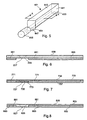
- Fig. 6 is a schematic side view of a first alternative embodiment 600 of a contact image sensor scanner window 605 .
- a layer (an overlay) of non-stick material is attached to all or much of those portions of scanner window 605 opposite back surface 639 that are not in focal area 227 .
- the non-stick layer material is thinner than the focal depth of the focal optics so that focussing is not substantially affected.
- Using a thin layer also should not substantially change the mechanical path thickness of the scanner.
- focal area 227 is located on the non-coated portion of scanner window 605 . Applying the non-stick layer as in the embodiment shown in Fig. 6 can be used to improve the performance of existing contact image sensors without adjusting the internal optics.
- Non-stick material 661 is chosen to have a relatively low coefficient of friction with document 103 .
- Several materials may be used, for example, one or more of a fluoropolymer (e.g. , the polytetrafluorethylene TEFLON TM ), silicone, ultra high molecular weight polyethylene (UHMW-PE), and an acetal resin (e.g. , DELRIN®).
- Static dissipative materials also may be advantageously added, and many such dissipative materials are available, including carbon fibers and carbon powder.
- Non-stick material 661 is attached to scanner window 105 either by a deposition technique or adhesively.
- Fig. 7 shows a schematic cross-sectional side view of a second alternative embodiment 700 of a scanner window 705 , in which two layers of material have been applied to the side of scanner window 705 opposite back surface 739 .
- One of the overlays is of the non-stick material, and the thickness of the non-stick material overlay may be greater than the focal depth of the focusing optics.
- a light transmitting material overlay 773 covers an area preferably greater than the focal area, shown as 727 , and a non-stick material overlay 771 covers the remaining area of scanner window outer surface 737 .
- the focal area edge rays are shown as 735 .
- Light transmitting material 773 is a scratch resistant, transparent material, with appropriate materials including acrylic and CR-39®.
- Non-stick material 771 is chosen to have a low coefficient of friction with document 103 , and appropriate materials include one or more of a fluoropolymer (e.g ., the polytetrafluorethylene TEFLON®), silicone, ultra high molecular weight polyethylene (UHMW-PE), a nylon, and an acetal resin (e.g., DELRIN®). Static dissipative material such as carbon fibers or carbon powder also may be advantageously added. Both light transmitting material 773 and non-stick material 771 are preferably adhesively attached to scanner window 705 , with optical properties chosen to minimize internal optical reflections during imaging.
- a fluoropolymer e.g ., the polytetrafluorethylene TEFLON®
- silicone silicone
- UHMW-PE ultra high molecular weight polyethylene
- nylon e.g., polyethylene
- an acetal resin e.g., DELRIN®
- Static dissipative material such as carbon fibers or carbon
- the thicknesses of light transmitting material 773 and non-stick material 771 are preferably substantially the same, presenting a smooth surface for scanning.
- the CIS focusing optics are positioned to bring the scanner window focal area, shown as 727 , into focus.
- Fig. 8 shows a schematic cross-sectional side view of a third alternative embodiment 800 of a scanner window 805 .
- This embodiment also is the one incorporated in the preferred embodiment of a CIS device shown in Fig. 4.
- Scanner window 805 includes recessed area 883 on the side opposite back surface 839 allowing for the insertion of an overlay of non-stick material 881 .
- the focal area edge rays are shown as 835 .
- Non-stick material 881 is chosen to have a low coefficient of friction with document 103 , and many materials are suitable, including one or more of a fluoropolymer (e.g., the polytetrafluorethylene TEFLON®), ultra high molecular weight polyethylene (UHMW-PE), silicone, a nylon, and an acetal resin (e.g. , DELRIN®). Static dissipative material such as carbon fibers or carbon powder also may be advantageously added. In the preferred embodiment of Fig. 4, the non-stick material 881 is part of integral housing 441 as described above.
- non-stick material 881 can be deposited on recess 883 , attached using a layer of adhesive or double-stick tape, or otherwise adhesively attached.
- non-stick material 881 is deposited (if deposition is used) or fabricated (if the material is adhesively applied) so that it fits into scanner window recess 883 providing a surface flush with focal area 827 .
- Scanner window recess 883 includes most of the area of scanner window 805 , but does not include any of focal area 827 , as this would interfere with document imaging.
- Focal area 827 is completely contained within that area not included in recess 883 .
- edges of the materials in contact with document 103 are rounded (smoothed) in order to enhance the non-stick performance.
Landscapes
- Engineering & Computer Science (AREA)
- Multimedia (AREA)
- Signal Processing (AREA)
- Facsimile Scanning Arrangements (AREA)
- Mechanical Optical Scanning Systems (AREA)
- Combination Of More Than One Step In Electrophotography (AREA)
- Facsimile Heads (AREA)
Abstract
Description
- The invention relates to an apparatus for scanning a document according to the preamble of claim 1, and in particular the design and implementation of contact image sensors in scanning devices to allow for the scanning of photographic paper, specifically by reducing the sliding friction of the scanner window surface.
- An apparatus of the initially-mentioned type is known, e.g., from
EP-A-0 603 903 . - High-quality "scanning" of physical documents such as business documents into digital form is routinely accomplished in commercially available devices such as computer-attached document scanners and facsimile machines. Document scanners are used to convert images to digital form for inclusion in computer files. Facsimile machines transmit the digital information over telephone lines to other facsimile machines, which then recreate the original document. The conversion of the document from physical to digital form is accomplished in an image sensor unit. Traditionally, the image sensor is a charge coupled device (CCD) or a silicon image sensor. Illumination is provided by an illuminating device, while the optics for focusing from the surface of the document to the image sensor is provided with mirror(s) and lenses.
- Recently, a compact integrated device, called a contact image sensor (CIS) has started to be used for the image sensor unit. A CIS typically incorporates illumination, focusing optics in the form of a narrow depth of focus lens array, and sensor arrays in one package. The narrow depth of focus lens array optics usually is a gradient index fiber optic array. The compact unit is often sealed, with illumination and document scanning occurring through a single "scanner window." Scanning devices are constructed so that the CIS image sensor unit scans the width of the document, which is placed at the focus of the unit, while the length of the document is scanned by inducing relative motion between the document and the sensor unit. The advantages of a CIS device over traditional sensor technology include: ease of manufacturing, reduced component count, fewer moving parts, reduced cost, integrated optics, and environmentally controlled optical path.
- The relative motion between the document and the image sensor unit is obtained through one of two configurations. The first typically is used by "flat bed" scanners and copiers. In such a configuration, the CIS usually does not have a physical scanner window, and the document is placed on top of a sheet of transparent material, usually a glass platen, with an image scanner located below and focused through the transparent material. The CIS image scanner unit is forced to move the length of the document through a drive mechanism while the document remains stationary. This configuration is not the main area of application of the present invention.
- A second configuration is suitable for use in facsimile machines, hand-held scanners and sheet-fed scanners, and is the main area of application of the present invention. In such a configuration, the CIS unit is arranged so that the focus of the sensor-lens system is coincident with the outer surface of a window that is fixed to the CIS. The document must be placed essentially in contact with the scanner window for the document to be in focus, and such a short (essentially zero) document-to-sensor window distance must be maintained while scanning. Because of the utility of this arrangement, sealed contact image sensors are common in facsimile machines and other inexpensive document scanners, and devices that use them must be configured so that the document to be scanned slides across the scanner window.
- The contact image sensor arrangement has several advantages. Image sensor units are relatively durable and low cost, resulting in the near ubiquity of facsimile machines, and in the low cost of black and white or gray scale document scanners. Contact image sensors usually have a very small depth of focus however, on the order of two tenths of a millimeter, and so reliable scanning is accomplished only with a document in good contact with the scanner window. The relatively narrow depth of field of contact image sensors results in design problems that are not present in image sensors where the depth of field can be varied. The recent introduction of color contact image sensors provides yet another design problem: color scanners are used for photographs as well as printed documents, and thus the contact image sensor must be compatible with photographic media. Contact is not a problem with many types of common document material, such as smooth paper. However, scanners based on contact image sensors technology suffer from the inability to scan materials that cannot pass smoothly by the scanner unit. Specifically, photographic documents cannot reliably be used with contact image sensors. This inability manifests itself in the following ways:
- 1. Due to the soft, water absorbing properties of photographic emulsions, "wetted" contact between the photographic document and the scanner window may occur. When this happens, the coefficient of friction between the document and scanner window is increased, the document sticks to the scanner window, and document transport problems result.
- 2. The optical properties of the document/scanner window interface vary between wetted and non-wetted contact points. The partial sticking of the photographic document to the window results in streaks or spots on the scanned image which is denoted here as "spotting."
- 3. Soft photographic emulsions are much more susceptible to damage than are paper documents. Photographic documents may be harmed or scratched as a result of either the direct contact of the sliding contact with the window, or by dirt (or other) particles that may come between the document and the scanner window.
- Thus there is a need in the art for overcoming the problems encountered with scanning by CISs of documents, such as photographs, that may stick to the scanner window.
- The reason for the problems encountered with CIS scanning of photographs, as enumerated above, has to do with the interaction between soft photographic emulsions and the scanner window surface. In order to improve the utility of scanners by including the ability to handle photographs, in one aspect of the invention, a modification to the design of a traditional scanner window is proposed. Specifically, the modification includes reducing the amount of friction between the document and the outer surface of the scanner window, thus enabling contact image sensors to work for photographs with the same reliability and ease with which they work with paper and other document materials.
- One object of the present invention is to allow CIS scanning to be useful in scanning documents that have the propensity to stick to the scanner window.
- Another object of the invention is to reduce the incidence of document jamming that occurs during CIS scanning of photographic or similar documents.
- Another object is to reduce the incidence of spotting that occurs during the CIS scanning of photographic or similar documents.
- Another object is to reduce the incidence of scratching of documents that occurs during the CIS scanning of photographic or similar documents.
- While some elements to reduce friction have been described herein, the adding of other friction reducing elements within the scope of the invention will become clear to those of ordinary skill in the art, and this invention is not limited to the specific methods and apparatuses described herein. In addition, while this invention is designed for the scanning of photographs, it is also generally useful in all scanning applications where sliding contact occurs, and thus where a reduction in sliding friction is advantageous.
- According to one aspect of the present invention, the foregoing and other objects and advantages are attained by including modifications to a prior art scanner window to reduce friction with the document.
- According to another aspect of the present invention, the foregoing and other objects and advantages are attained by including a scanner window which has a low coefficient of sliding friction with the document.
- In accordance with yet another aspect of the invention, the scanner window is recessed in areas away from the focal area of the CIS unit to allow for the addition of non-slip material in those areas, while not interfering with the focus of the CIS optics.
- In accordance with yet another aspect of the invention, the scanner window is recessed in areas away from the focal area of the CIS unit and includes non-slip material in those areas.
- In accordance with yet another aspect of the invention, the scanner window is coated with a combination of light-transmitting and non-stick materials to allow for the smooth passage of the document over the CIS unit, and the transmission of the document image to the sensor array, the optics adapted to focus through the coating.
- In accordance with yet another aspect of the invention, the non-focal area portion of the scanner window is coated with a layer of non-stick material that is less than the focal depth of the scanner optics.
- The present invention will be more fully understood from the detailed preferred embodiments of the invention, which, however, should not be taken to limit the invention to any specific embodiment but are for explanation and better understanding only. The embodiments in turn are explained with the aid of the following figures:
- Fig. 1 is a perspective view of a contact image sensor traversing a document;
- Fig. 2 is a schematic cross-sectional side view (section A-A of Fig. 1) of a contact image sensor as used in scanners and facsimile machines;
- Fig. 3 is a top view of a contact image sensor on a document showing the outline of the scanner window, the focal-area and the non-focal area;
- Fig. 4 is a schematic side view of the preferred embodiment of a contact image sensor with an integrated light source-scanner window, showing the features according to the present invention;
- Fig. 5 is a perspective view of the preferred embodiment for an integral housing unit;
- Fig. 6 is a schematic side view of the first alternative embodiment of a contact image sensor scanner window showing features according to the present invention;
- Fig. 7 is a schematic side view of the second alternative embodiment of a contact image sensor scanner window showing features according to the present invention.
- Fig. 8 is a schematic side view of the third alternative embodiment of a contact image sensor scanner window showing features according to the present invention.
-
- 101
- Contact Image Scanner (CIS)
- 103
- Document
- 105
- Scanner Window
- 107
- Sensor Array Output
- 109
- Output Electronics
- 111
- CIS Output
- 113
- Power Supply
- 221
- Outer Housing or Cover
- 223
- Light Source
- 225
- Focusing Optics
- 227
- Focal Area
- 229
- Sensor Array
- 231
- Substrate
- 233
- Non-Focal Area
- 235
- cal Area Edge Rays
- 237
- Scanner Window Outer Surface
- 239
- Scanner Window Back Surface
- 401
- Contact Image Scanner (CIS)
- 405
- Scanner Window
- 423
- Illumination Unit Housing
- 427
- Focal Area
- 433
- Non-Focal Area
- 441
- Integral Housing
- 443
- Housing Scanning Surface
- 445
- Integral Housing Back Cover
- 447
- Roller
- 449
- Protruding Part of Integral Housing Unit
- 451
- Flange
- 453
- Flange
- 455
- Drive Motor
- 600
- a first alternative embodiment of a contact image sensor scanner window
- 605
- Scanner Window
- 639
- Scanner Window Back Surface
- 661
- Non-Stick Material
- 700
- a second alternative embodiment of a contact image sensor scanner window
- 705
- Scanner Window
- 727
- Focal Area
- 735
- Focal Area Edge Rays
- 737
- Scanner Window Outer Surface
- 739
- Scanner Window Back Surface
- 771
- Non-Stick Material
- 773
- Light Transmitting Material
- 800
- a third alternative embodiment of a contact image sensor scanner window
- 805
- Scanner Window
- 827
- Focal Area
- 835
- Focal Area Edge Rays
- 839
- Scanner Window Back Surface
- 881
- Non-Stick Material
- 883
- Scanner Window Recess
- Fig. 1 shows a perspective view of a typical contact image sensor (CIS) 101 traversing a document. While a CIS such as
CIS 101 shown in Fig. 1 is prior art, and hence is so labeled, a CIS with the friction reducing modifications described herein and a CIS with the reduced friction elements described herein are not prior art.CIS 101 is positioned for scanning adocument 103 by placing thetransparent scanner window 105 substantially in contact withdocument 103 and producing relative motion betweenCIS 101 anddocument 103. Byscanner window 105 being substantially in contact withdocument 103 is meant that the distance betweenscanner window 105 anddocument 103 is very small so that the document remains in focus even given the narrow depth of field of the optics inCIS 101.Typical CIS 101 components are compact, and document 103 is scanned in a direction perpendicular to the CIS length direction. Relative motion may occur by either moving the CIS over a fixed document, or by moving the document over a fixed CIS. As would be clear to one in the art, necessary electrical connections for the operation ofCIS 101 include apower supply 113, andelectronics 109 which convert theCIS output 107 to auseful output 111.Elements - Fig. 2 shows a schematic cross-sectional side view of a
typical CIS 101, which is shown as section A-A in Fig. 1. The size and placement of the components in cross sectional view are approximately the same at any location down the length of the CIS. Again, while Fig. 2 is labeled "prior art," a CIS with the friction reducing modifications described herein and a CIS with the reduced friction elements described herein are not prior art.CIS 101 is shown in Fig. 2 in the proper position for scanningdocument 103. The CIS components are contained within an outer housing or cover 221 andtransparent scanner window 105.Scanner window 105 has anouter surface 237 facingdocument 103 during scanning, and aback surface 239 facingsensor array 229. The components that are important in scanning are alight source 223, focusingoptics 225, and asensor array 229.Scanner window 105,optics 225,sensor array 229 andlight source 223 are all approximately the same length in a typical CIS.Sensor array 229 is part of asubstrate 231 which contains electronics for controlling data flow from the output ofsensor array 229, producingCIS output 107, shown in Fig. 1. -
Light source 223 includes a light producing unit, such as an incandescent light or a set of light emitting diodes, with or without a light pipe, that produces light that is projected along the length ofCIS 101 and towardsscanner window 105. It is important thatlight source 223 illuminates at least part ofdocument 103 with enough reflected light forsensor array 229 to produce a useful signal. Focusingoptics 225, which can consist of a combination of lenses and mirrors or, as is typical in a CIS, a narrow depth of focus lens array such as a gradient index array (also called a self-focussing lens array, e.g., SELFOC Lens Array by Nippon Steel Glass Co., Tokyo, Japan), transfers the image ofdocument 103, positioned againstscanner window 105, ontosensor array 229. In a typical CIS scanner, focusingoptics 225 have a very narrow depth of field, typically less than one millimeter, and focussingoptics 225 are adapted to focus an area (called thefocal area 227 herein) on the scanner windowouter surface 237. For focused scanning,document 103 must be in contact with or close to being in contact with scanner windowouter surface 237.Focal area 227 is typically approximately one millimeter wide and has a length determined by the design of focusing optics. The trace of the edge of focal area optical rays fromfocal area 227 tosensor array 229 are shown as focal area edge rays 235. The area ofscanner window 105 that is not infocal area 227 is termed the non-focal area herein withreference numeral 233. Thus each point on scanner windowouter surface 237 is in eitherfocal area 227 ornon-focal area 233. - The internal structure of some components, for example,
components - Fig. 3 shows a top view of
document 103 with projections ofscanner window 105,focal area 227 andnon-focal area 233. The scanned area ofdocument 103 is that area traced out byfocal area 227 during the relative motion of the CIS anddocument 103. - The features of the present invention may be incorporated into several embodiments of CIS devices.
- Fig. 4 is a schematic side view of one embodiment of a
contact image sensor 401 which includes features according to the present invention. The CIS includes anintegral housing 441 that includes ahousing scanning surface 443 substantially in contact withdocument 103, up to but not including thefocal area 427 leaving an opening in the front (i.e., document) side ofintegral housing unit Integral housing 441 is made of a combination of non-stick and static dissipative materials in a plastic binder base material. Any material that reduces the friction with the document during scanning will do for the non-stick material, and preferably, the non-stick material has a substantially lower coefficient of friction with the document than does the scanner window. Many non-stick materials may be used. For example, one can use one or more of a fluoropolymer (e.g., the polytetrafluorethylene TEFLON® from E.I. du Pont de Nemours and Company, Wilmington, Delaware), silicone, ultra high molecular weight polyethylene (UHMW-PE) (Crown Plastics, Harrison, Ohio), and a polymer such as nylon. Static dissipative materials to use include adding carbon fibers or carbon powder. Many materials are suitable for use as the base material, including polycarbonate, nylon, and an acetal resin (e.g., DELRIN® from E.I. du Pont de Nemours and Company, Wilmington, Delaware). Note nylon and the acetal resin already have a low coefficient of friction. Glass may also be added for mechanical strength. In the preferred embodiment, an available compound of polycarbonate with 30% carbon fiber. 13% TEFLON, and 2% silicone is used (Part Number J-50/CF/30/TF/13/SI/2 from Dutch State Mining of the Netherlands or DSM Engineering Plastics, Inc., Evansville Indiana).Integral housing 441 is formed with an integral housingback cover 445 as a separate piece to allow for easy mounting of the CIS components.Scanner window 405 is located interior to and against the front (document) side ofintegral housing unit 441, and thus has aprotruding part 449 that fits in the opening of the front side ofhousing unit 441. A portion of protrudingpart 449, called the scanner window scanning surface herein, is flush withhousing surface 443, contains thefocal area 427 andnon-focal area 433, and is arranged to allow sufficient lighting from anillumination unit 423 throughfocal area 427.Scanner window 405 is made of clear glass, or a scratch resistant, transparent material, such as acrylic or clear polycarbonate or a clear thermosetting monomer such as allyl diglycol carbonate (e.g., CR-39® from PPG Industries, Inc. of Pittsburgh, Pennsylvania). In the preferred embodiment, clear acrylic is used because of the ease of co-molding the window material with the non-stick material compound.Integral housing unit 441 andscanner window 405 are preferably formed into a compact scanner design byco-molding scanner window 405 intointegral housing 441. - Having the whole body made of a material which has a low coefficient of friction with
document 103 solves one of the problems of prior art CIS devices when used, for example, for scanning photographs. Adding static electricity dissipative materials, such as carbon filled fibers, also reduces any sticking between the CIS and document 103 that may occur because of the attraction forces resulting from static electricity. - A perspective view of the preferred embodiment of
integral housing unit 441 is shown in Fig. 5. Fig. 4 is the section A-A of Fig. 5. To simplify manufacture, each end of the CIS housing includes a flange, shown asflanges roller 447. One flange,flange 451, also includes the mounting for a drive motor, the motor indicated byreference numeral 455. - To improve document illumination and to reduce manufacturing costs,
scanner window 405 is integrated and optically coupled toillumination unit 423 and acts as a light pipe thereto, hence reducing the number of parts in the embodiment ofCIS 401 while producing a mechanism with the same function.Document 103 is held against integralhousing scanning surface 443 by aroller 447.Roller 447 is slightly offset fromfocal area 427, thus reducing the contact pressure betweendocument 103 andscanner window 405 and resulting in decreased contact related imaging problems. Conventional prior-art implementation scanners using a CIS often include a roller for maintaining contact between the document and the scanner window, and typically such a roller may be positioned to impart a force on the document forcing the document against the focal area. The improvement in the embodiment of Fig. 4 includespositioning roller 447 to impart its force on the non-focal area rather than the focal area, thus reducing the likelihood of sticking problems in the focal area. Such an improvement may also be applied to the other embodiments disclosed herein. - The improvement in the embodiment of Fig. 4 of having
scanner window 405 integrated and optically coupled to thelight illumination unit 423, and acting as a light pipe thereto, may also be incorporated into any of the other embodiments described herein. - Alternate embodiments of the scanner window are now discussed. Each of these embodiments may be used to modify the design of a conventional CIS-based scanner such as that of Figs. 1 and 2 or to design a new CIS-based scanner.
- Fig. 6 is a schematic side view of a first alternative embodiment 600 of a contact image
sensor scanner window 605. A layer (an overlay) of non-stick material is attached to all or much of those portions ofscanner window 605opposite back surface 639 that are not infocal area 227. The non-stick layer material is thinner than the focal depth of the focal optics so that focussing is not substantially affected. Using a thin layer also should not substantially change the mechanical path thickness of the scanner. As shown in Fig. 6,focal area 227 is located on the non-coated portion ofscanner window 605. Applying the non-stick layer as in the embodiment shown in Fig. 6 can be used to improve the performance of existing contact image sensors without adjusting the internal optics.Non-stick material 661 is chosen to have a relatively low coefficient of friction withdocument 103. Several materials may be used, for example, one or more of a fluoropolymer (e.g., the polytetrafluorethylene TEFLON™), silicone, ultra high molecular weight polyethylene (UHMW-PE), and an acetal resin (e.g., DELRIN®). Static dissipative materials also may be advantageously added, and many such dissipative materials are available, including carbon fibers and carbon powder.Non-stick material 661 is attached toscanner window 105 either by a deposition technique or adhesively. - Fig. 7 shows a schematic cross-sectional side view of a second alternative embodiment 700 of a
scanner window 705, in which two layers of material have been applied to the side ofscanner window 705opposite back surface 739. One of the overlays is of the non-stick material, and the thickness of the non-stick material overlay may be greater than the focal depth of the focusing optics. A light transmittingmaterial overlay 773 covers an area preferably greater than the focal area, shown as 727, and anon-stick material overlay 771 covers the remaining area of scanner windowouter surface 737. The focal area edge rays are shown as 735.Light transmitting material 773 is a scratch resistant, transparent material, with appropriate materials including acrylic and CR-39®.Non-stick material 771 is chosen to have a low coefficient of friction withdocument 103, and appropriate materials include one or more of a fluoropolymer (e.g., the polytetrafluorethylene TEFLON®), silicone, ultra high molecular weight polyethylene (UHMW-PE), a nylon, and an acetal resin (e.g., DELRIN®). Static dissipative material such as carbon fibers or carbon powder also may be advantageously added. Bothlight transmitting material 773 andnon-stick material 771 are preferably adhesively attached toscanner window 705, with optical properties chosen to minimize internal optical reflections during imaging. The thicknesses oflight transmitting material 773 andnon-stick material 771 are preferably substantially the same, presenting a smooth surface for scanning. As with the previously described embodiments, the CIS focusing optics are positioned to bring the scanner window focal area, shown as 727, into focus. - Fig. 8 shows a schematic cross-sectional side view of a third alternative embodiment 800 of a
scanner window 805. This embodiment also is the one incorporated in the preferred embodiment of a CIS device shown in Fig. 4.Scanner window 805 includes recessedarea 883 on the side opposite backsurface 839 allowing for the insertion of an overlay ofnon-stick material 881. The focal area edge rays are shown as 835.Non-stick material 881 is chosen to have a low coefficient of friction withdocument 103, and many materials are suitable, including one or more of a fluoropolymer (e.g., the polytetrafluorethylene TEFLON®), ultra high molecular weight polyethylene (UHMW-PE), silicone, a nylon, and an acetal resin (e.g., DELRIN®). Static dissipative material such as carbon fibers or carbon powder also may be advantageously added. In the preferred embodiment of Fig. 4, thenon-stick material 881 is part ofintegral housing 441 as described above. In other realizations,non-stick material 881 can be deposited onrecess 883, attached using a layer of adhesive or double-stick tape, or otherwise adhesively attached. In addition,non-stick material 881 is deposited (if deposition is used) or fabricated (if the material is adhesively applied) so that it fits intoscanner window recess 883 providing a surface flush withfocal area 827.Scanner window recess 883 includes most of the area ofscanner window 805, but does not include any offocal area 827, as this would interfere with document imaging.Focal area 827 is completely contained within that area not included inrecess 883. - In another aspect of the invention, applicable to all embodiments described above, the edges of the materials in contact with
document 103 are rounded (smoothed) in order to enhance the non-stick performance. - Hence, although this invention has been described with respect to preferred embodiments, those embodiments are illustrative only. No limitation with respect to the preferred embodiments is intended or should be inferred. It will be observed that numerous variations and modifications may be effected without departing from the true spirit and scope of the novel concept of the invention. For example, different materials may be used to produce low friction or the dissipation of static electricity or both, and the materials may be applied in different ways or be integral with the housing or parts thereof. It is intended that the scope of the invention be defined by the claims appended hereto.
Claims (19)
- Apparatus for scanning documents (103), the apparatus comprising:(a) a contact image sensor (401) (CIS) enclosed in a housing (441), the CIS comprising:(i) a light-sensitive sensor array, having an output,(ii) a scanner window (405, 605, 705, 805) substantially in contact with the document (103) during scanning, said scanner window (405, 605, 705, 805) having an outer surface and a back surface, the back surface oriented towards the sensor array;(iii) an opening in said housing (441) adapted to contain the scanner window (405, 605, 705, 805),(iv) optics positioned between the scanner window (405, 605, 705, 805) and the sensor array, the optics adapted to focus a focal area (427, 827) of the outer surface onto the sensor array, the focusing being with a focal depth region, the focal area (427, 827) being that portion of the outer surface within the focal depth region, the balance of the outer surface being at least part of a non-focal area (433); and(v) a light source adapted to illuminate at least part of the focal area (427, 827);(b) electronics coupled to the sensor array output to convert the sensor array output to a useful signal, and(c) supply electronics coupled to the light source for controlling the light source,wherein the scanner window (405, 605, 705, 805) outer surface includes a portion of the focal area (427, 827) within the focal depth region, the improvement comprising:one or more alterations to the scanner window (405, 605, 705, 805) to reduce the friction between the scanner window (405, 605, 705, 805) and the document (103),characterized in that said alterations comprise:(1) a recess of the scanner window (405, 605, 705, 805), comprising a portion of the non-focal area (433), having a thickness greater than the focal depth of the optics,(2) a non-stick material (661, 771, 881), having a non-stick material (661, 771, 881) outer surface facing the document (103), the non-stick material (661, 771, 881) having approximately the thickness and area of said recess, the non-stick material (661, 771, 881) selected to have a lower coefficient of friction with the document (103) than does the scanner window (405, 605, 705, 805) material, and(3) means for attaching the non-stick material (661, 771, 881) to the recess.
- Apparatus for scanning documents according to claim 1, wherein the optics is a narrow depth of focus lens array.
- Apparatus for scanning documents according to claim 1, wherein the document (103) includes a photographic emulsion.
- Apparatus for scanning documents according to claim 1, wherein the non-stick material (661, 771, 881) is static electricity dissipative.
- Apparatus for scanning documents according to claim 4, wherein the non-stick material (661, 771, 881) includes a fluoropolymer, silicone, ultra high molecular weight polyethylene, an acetate resin, or nylon.
- Apparatus for scanning documents according to claim 5, wherein said non-stick material (661, 771, 881) is composed of a combination of materials, the combination including:(i) a fluoropolymer, silicone, ultra high molecular weight polyethylene, an acetate resin, or nylon, and(ii) carbon fibers or carbon powder.
- Apparatus for scanning documents according to one of the preceding claims, wherein the edges of elements substantially contacting the document (103) during scanning are rounded.
- Apparatus for scanning documents according to claim 1 comprising:(a) a light transmitting material composed of a substantially light transmitting material applied to a first area, said first area being on the scanner window (405, 605, 705, 805)
and including the focal area (427, 827), and said first area having an outer surface facing the document (103),(b) an adaptation of the optics to provide for focusing on the light transmitting material outer surface,(c) a non-stick material (661, 771, 881) applied to a second area, said second area on the scanner window (405, 605, 705, 805) and including at least part of the non-focal area (433), the non stick material selected to have a lower coefficient of friction with the document (103) than does the scanner window (405, 605, 705, 805) material,(d) means for attaching the light transmitting material to the scanner window (405, 605, 705, 805) first area, and(e) means for attaching the non-stick material (661, 771, 881) to the scanner window (405, 605, 705, 805) second area. - Apparatus for scanning documents according to claim 8, wherein said light transmitting material is a scratch resistant material
- Apparatus for scanning documents according to claim 8, wherein the non-stick material (661, 771, 881) is static electricity dissipative.
- Apparatus for scanning documents according to claim 8, wherein the non-stick material (661, 771, 881) includes a fluoropolymer, silicone, ultra high molecular weight polyethylene, an acetate resin, or nylon.
- Apparatus for scanning documents according to claim 10, wherein said non-stick material (661, 771, 881) is composed of a combination of materials, the combination including:(i) a fluoropolymer, silicone, ultra high molecular weight polyethylene, an acetate resin, or nylon, and(ii) carbon fibers or carbon powder.
- Apparatus for scanning documents according to claim 8, wherein the edges of elements substantially contacting the document (103) during scanning are rounded.
- Apparatus for scanning documents according to claim 1 comprising :(a) a non-stick material (661, 771, 881) applied to at least part of the non-focal area (433), the non stick material having approximately a thickness less than the focal depth of the optics, and(b) means of attaching the non-stick material (661, 771, 881) to the scanner window (405, 605, 705, 805), the non stick material selected to have a lower coefficient of friction with the document (103) than does the scanner window (405, 605, 705, 805) material.
- Apparatus for scanning documents according to claim 14, wherein the non-stick material (661, 771, 881) is static electricity dissipative.
- Apparatus for scanning documents according to claim 14, wherein the non-stick material (661, 771, 881) includes a fluoropolymer, silicone, ultra high molecular weight polyethylene, an acetate resin, or nylon
- Apparatus for scanning documents according to claim 15, wherein said non-stick material (661, 771, 881) is composed of a combination of materials, the combination including:(i) a fluoropolymer, silicone, ultra high molecular weight polyethylene, an acetate resin, or nylon, and(ii) carbon fibers or carbon powder.
- Apparatus for scanning documents according to claim 14, wherein the edges of elements substantially contacting the document (103) during scanning are rounded.
- Apparatus for scanning documents according to claim 1, wherein the contact image sensor (401) (CIS) device further comprising:a scanner window (405, 605, 705, 805) overlay attached to the scanner window (405, 605, 705, 805), the overlay substantially contacting the document (103) during scanning, and having a relatively low coefficient of friction with the document (103) during scanning.
Applications Claiming Priority (3)
| Application Number | Priority Date | Filing Date | Title |
|---|---|---|---|
| US09/118,693 US6154294A (en) | 1998-07-16 | 1998-07-16 | Apparatus for scanning documents such as photographs using a contact image sensor |
| US118693 | 1998-07-16 | ||
| PCT/US1999/015970 WO2000004703A2 (en) | 1998-07-16 | 1999-07-14 | Contact image sensor scanner for photograph documents |
Publications (3)
| Publication Number | Publication Date |
|---|---|
| EP1114551A2 EP1114551A2 (en) | 2001-07-11 |
| EP1114551A4 EP1114551A4 (en) | 2006-05-03 |
| EP1114551B1 true EP1114551B1 (en) | 2008-01-02 |
Family
ID=22380176
Family Applications (1)
| Application Number | Title | Priority Date | Filing Date |
|---|---|---|---|
| EP99937255A Expired - Lifetime EP1114551B1 (en) | 1998-07-16 | 1999-07-14 | Improved apparatus for scanning documents such as photographs using a contact image sensor |
Country Status (8)
| Country | Link |
|---|---|
| US (1) | US6154294A (en) |
| EP (1) | EP1114551B1 (en) |
| CN (1) | CN1186920C (en) |
| AT (1) | ATE383029T1 (en) |
| DE (1) | DE69937889T2 (en) |
| MY (1) | MY133150A (en) |
| TW (1) | TW427090B (en) |
| WO (1) | WO2000004703A2 (en) |
Families Citing this family (10)
| Publication number | Priority date | Publication date | Assignee | Title |
|---|---|---|---|---|
| US6426498B1 (en) * | 2000-04-03 | 2002-07-30 | Hewlett-Packard Co. | Optics module for optical scanning device |
| US6785024B1 (en) * | 2000-08-17 | 2004-08-31 | Eastman Kodak Company | Digital scanner |
| US6822766B2 (en) | 2001-03-01 | 2004-11-23 | Hewlett-Packard Development Company, L.P. | Correction for debris and low output photosensors in scroll fed scanner using stored initial calibration data |
| TW552794B (en) * | 2001-03-02 | 2003-09-11 | Nippon Sheet Glass Co Ltd | Image reading apparatus |
| US7128415B2 (en) * | 2003-04-30 | 2006-10-31 | Polylite Taiwan Company, Ltd | Method of forming polarized or photochromic lenses by fusing polycarbonate with other plastic materials |
| TWM244293U (en) * | 2003-11-21 | 2004-09-21 | Benq Corp | Automatic feeding apparatus |
| TWI496450B (en) * | 2010-04-07 | 2015-08-11 | Creative Sensor Inc | Lighting module and the contact image sensor using the same |
| JP5937055B2 (en) * | 2013-12-19 | 2016-06-22 | キヤノンファインテック株式会社 | Image reading apparatus and image forming apparatus having the same |
| CN104102395B (en) * | 2014-07-03 | 2017-12-15 | 宁波术有电子科技有限公司 | The implementation method of wide format images scanning system based on gigabit Ethernet transmission |
| US10630862B2 (en) * | 2016-09-08 | 2020-04-21 | Hewlett-Packard Development Company, L.P. | Transparent platen with chamfered egress edge |
Family Cites Families (6)
| Publication number | Priority date | Publication date | Assignee | Title |
|---|---|---|---|---|
| US5196691A (en) * | 1989-11-21 | 1993-03-23 | Canon Kabushiki Kaisha | Photoelectric converting device having original conveyance guide and an image processing apparatus incorporating the device |
| GB2252333B (en) * | 1991-01-29 | 1995-07-19 | Spectra Physics Scanning Syst | Improved scanner window |
| US5412490A (en) * | 1991-07-09 | 1995-05-02 | Oki Electric Industry Co., Ltd. | Printer provided with an image reading unit |
| JP2696025B2 (en) * | 1991-11-18 | 1998-01-14 | 沖電気工業株式会社 | Read head |
| JP3067435B2 (en) * | 1992-12-24 | 2000-07-17 | キヤノン株式会社 | Image reading photoelectric conversion device and image processing apparatus having the device |
| GB2289885B (en) * | 1994-05-26 | 1998-06-17 | Primax Electronics Ltd | Scanning device |
-
1998
- 1998-07-16 US US09/118,693 patent/US6154294A/en not_active Expired - Lifetime
-
1999
- 1999-07-14 WO PCT/US1999/015970 patent/WO2000004703A2/en not_active Ceased
- 1999-07-14 EP EP99937255A patent/EP1114551B1/en not_active Expired - Lifetime
- 1999-07-14 DE DE69937889T patent/DE69937889T2/en not_active Expired - Lifetime
- 1999-07-14 AT AT99937255T patent/ATE383029T1/en not_active IP Right Cessation
- 1999-07-14 CN CNB998090174A patent/CN1186920C/en not_active Expired - Fee Related
- 1999-07-16 MY MYPI99003009A patent/MY133150A/en unknown
- 1999-07-22 TW TW088112047A patent/TW427090B/en not_active IP Right Cessation
Also Published As
| Publication number | Publication date |
|---|---|
| MY133150A (en) | 2007-10-31 |
| WO2000004703A3 (en) | 2000-04-20 |
| CN1186920C (en) | 2005-01-26 |
| TW427090B (en) | 2001-03-21 |
| WO2000004703A2 (en) | 2000-01-27 |
| EP1114551A2 (en) | 2001-07-11 |
| US6154294A (en) | 2000-11-28 |
| CN1310911A (en) | 2001-08-29 |
| DE69937889T2 (en) | 2009-01-02 |
| EP1114551A4 (en) | 2006-05-03 |
| ATE383029T1 (en) | 2008-01-15 |
| DE69937889D1 (en) | 2008-02-14 |
Similar Documents
| Publication | Publication Date | Title |
|---|---|---|
| KR100491499B1 (en) | Structure for preventing extraneous light from entering image reading apparatus | |
| US8643917B2 (en) | Light projection unit, image reading device including same, and image forming apparatus including the image reading device | |
| KR100336809B1 (en) | Contact type image sensor and information processing apparatus | |
| US6767122B2 (en) | Light guide, line illumination apparatus, and image acquisition system | |
| CN1269093A (en) | Image sensor substrate and image sensor employing same | |
| US6154294A (en) | Apparatus for scanning documents such as photographs using a contact image sensor | |
| US8279499B2 (en) | Single LED dual light guide | |
| EP1104623B1 (en) | Method and apparatus for keeping a document in focus during noncontact scanning | |
| US4987499A (en) | Image reading device | |
| US5027424A (en) | Image reader | |
| US8416472B2 (en) | LED light guide with integral IR filter | |
| US7055743B2 (en) | End-of-travel focus shift in an optical image scanner | |
| US20080173799A1 (en) | Optical element for a document illuminator | |
| GB2398954A (en) | Scanning different image planes using dual sensors | |
| US20040164164A1 (en) | Systems and methods for providing multiple object planes in an optical image scanner | |
| WO2000048387A1 (en) | Image sensor and transparent cover for image sensor | |
| JP3912544B2 (en) | Image reading device | |
| JPH07183996A (en) | Reader | |
| US7158737B2 (en) | Carriage structure for image-reading device | |
| JP3007287B2 (en) | Scanning device | |
| US20070146815A1 (en) | Image capturing apparatus and focusing method thereof | |
| US20040164151A1 (en) | Systems and methods for providing multiple object planes in an optical image scanning environment | |
| JPS6229942B2 (en) | ||
| JPH06217080A (en) | Image sensor | |
| JPH0748789B2 (en) | Image reader |
Legal Events
| Date | Code | Title | Description |
|---|---|---|---|
| PUAI | Public reference made under article 153(3) epc to a published international application that has entered the european phase |
Free format text: ORIGINAL CODE: 0009012 |
|
| 17P | Request for examination filed |
Effective date: 20010206 |
|
| AK | Designated contracting states |
Kind code of ref document: A2 Designated state(s): AT BE CH CY DE DK ES FI FR GB GR IE IT LI LU MC NL PT SE |
|
| RAP1 | Party data changed (applicant data changed or rights of an application transferred) |
Owner name: SILITEK CORPORATION |
|
| A4 | Supplementary search report drawn up and despatched |
Effective date: 20060322 |
|
| 17Q | First examination report despatched |
Effective date: 20060829 |
|
| RAP1 | Party data changed (applicant data changed or rights of an application transferred) |
Owner name: LITE-ON TECHNOLOGY CORPORATION |
|
| GRAP | Despatch of communication of intention to grant a patent |
Free format text: ORIGINAL CODE: EPIDOSNIGR1 |
|
| GRAS | Grant fee paid |
Free format text: ORIGINAL CODE: EPIDOSNIGR3 |
|
| GRAA | (expected) grant |
Free format text: ORIGINAL CODE: 0009210 |
|
| AK | Designated contracting states |
Kind code of ref document: B1 Designated state(s): AT BE CH CY DE DK ES FI FR GB GR IE IT LI LU MC NL PT SE |
|
| REG | Reference to a national code |
Ref country code: GB Ref legal event code: FG4D |
|
| REG | Reference to a national code |
Ref country code: IE Ref legal event code: FG4D |
|
| REG | Reference to a national code |
Ref country code: CH Ref legal event code: EP |
|
| REF | Corresponds to: |
Ref document number: 69937889 Country of ref document: DE Date of ref document: 20080214 Kind code of ref document: P |
|
| PG25 | Lapsed in a contracting state [announced via postgrant information from national office to epo] |
Ref country code: NL Free format text: LAPSE BECAUSE OF FAILURE TO SUBMIT A TRANSLATION OF THE DESCRIPTION OR TO PAY THE FEE WITHIN THE PRESCRIBED TIME-LIMIT Effective date: 20080102 |
|
| NLV1 | Nl: lapsed or annulled due to failure to fulfill the requirements of art. 29p and 29m of the patents act | ||
| PG25 | Lapsed in a contracting state [announced via postgrant information from national office to epo] |
Ref country code: LI Free format text: LAPSE BECAUSE OF FAILURE TO SUBMIT A TRANSLATION OF THE DESCRIPTION OR TO PAY THE FEE WITHIN THE PRESCRIBED TIME-LIMIT Effective date: 20080102 Ref country code: FI Free format text: LAPSE BECAUSE OF FAILURE TO SUBMIT A TRANSLATION OF THE DESCRIPTION OR TO PAY THE FEE WITHIN THE PRESCRIBED TIME-LIMIT Effective date: 20080102 Ref country code: ES Free format text: LAPSE BECAUSE OF FAILURE TO SUBMIT A TRANSLATION OF THE DESCRIPTION OR TO PAY THE FEE WITHIN THE PRESCRIBED TIME-LIMIT Effective date: 20080413 Ref country code: CH Free format text: LAPSE BECAUSE OF FAILURE TO SUBMIT A TRANSLATION OF THE DESCRIPTION OR TO PAY THE FEE WITHIN THE PRESCRIBED TIME-LIMIT Effective date: 20080102 |
|
| REG | Reference to a national code |
Ref country code: CH Ref legal event code: PL |
|
| ET | Fr: translation filed | ||
| PG25 | Lapsed in a contracting state [announced via postgrant information from national office to epo] |
Ref country code: AT Free format text: LAPSE BECAUSE OF FAILURE TO SUBMIT A TRANSLATION OF THE DESCRIPTION OR TO PAY THE FEE WITHIN THE PRESCRIBED TIME-LIMIT Effective date: 20080102 |
|
| PG25 | Lapsed in a contracting state [announced via postgrant information from national office to epo] |
Ref country code: PT Free format text: LAPSE BECAUSE OF FAILURE TO SUBMIT A TRANSLATION OF THE DESCRIPTION OR TO PAY THE FEE WITHIN THE PRESCRIBED TIME-LIMIT Effective date: 20080602 Ref country code: BE Free format text: LAPSE BECAUSE OF FAILURE TO SUBMIT A TRANSLATION OF THE DESCRIPTION OR TO PAY THE FEE WITHIN THE PRESCRIBED TIME-LIMIT Effective date: 20080102 |
|
| PG25 | Lapsed in a contracting state [announced via postgrant information from national office to epo] |
Ref country code: SE Free format text: LAPSE BECAUSE OF FAILURE TO SUBMIT A TRANSLATION OF THE DESCRIPTION OR TO PAY THE FEE WITHIN THE PRESCRIBED TIME-LIMIT Effective date: 20080402 Ref country code: DK Free format text: LAPSE BECAUSE OF FAILURE TO SUBMIT A TRANSLATION OF THE DESCRIPTION OR TO PAY THE FEE WITHIN THE PRESCRIBED TIME-LIMIT Effective date: 20080102 |
|
| PLBE | No opposition filed within time limit |
Free format text: ORIGINAL CODE: 0009261 |
|
| STAA | Information on the status of an ep patent application or granted ep patent |
Free format text: STATUS: NO OPPOSITION FILED WITHIN TIME LIMIT |
|
| 26N | No opposition filed |
Effective date: 20081003 |
|
| PG25 | Lapsed in a contracting state [announced via postgrant information from national office to epo] |
Ref country code: MC Free format text: LAPSE BECAUSE OF NON-PAYMENT OF DUE FEES Effective date: 20080731 |
|
| PG25 | Lapsed in a contracting state [announced via postgrant information from national office to epo] |
Ref country code: IE Free format text: LAPSE BECAUSE OF NON-PAYMENT OF DUE FEES Effective date: 20080714 Ref country code: CY Free format text: LAPSE BECAUSE OF FAILURE TO SUBMIT A TRANSLATION OF THE DESCRIPTION OR TO PAY THE FEE WITHIN THE PRESCRIBED TIME-LIMIT Effective date: 20080102 |
|
| PG25 | Lapsed in a contracting state [announced via postgrant information from national office to epo] |
Ref country code: IT Free format text: LAPSE BECAUSE OF FAILURE TO SUBMIT A TRANSLATION OF THE DESCRIPTION OR TO PAY THE FEE WITHIN THE PRESCRIBED TIME-LIMIT Effective date: 20080102 |
|
| PG25 | Lapsed in a contracting state [announced via postgrant information from national office to epo] |
Ref country code: LU Free format text: LAPSE BECAUSE OF NON-PAYMENT OF DUE FEES Effective date: 20080714 |
|
| PG25 | Lapsed in a contracting state [announced via postgrant information from national office to epo] |
Ref country code: GR Free format text: LAPSE BECAUSE OF FAILURE TO SUBMIT A TRANSLATION OF THE DESCRIPTION OR TO PAY THE FEE WITHIN THE PRESCRIBED TIME-LIMIT Effective date: 20080403 |
|
| PGFP | Annual fee paid to national office [announced via postgrant information from national office to epo] |
Ref country code: DE Payment date: 20140707 Year of fee payment: 16 |
|
| PGFP | Annual fee paid to national office [announced via postgrant information from national office to epo] |
Ref country code: FR Payment date: 20140707 Year of fee payment: 16 Ref country code: GB Payment date: 20140707 Year of fee payment: 16 |
|
| REG | Reference to a national code |
Ref country code: DE Ref legal event code: R119 Ref document number: 69937889 Country of ref document: DE |
|
| GBPC | Gb: european patent ceased through non-payment of renewal fee |
Effective date: 20150714 |
|
| PG25 | Lapsed in a contracting state [announced via postgrant information from national office to epo] |
Ref country code: GB Free format text: LAPSE BECAUSE OF NON-PAYMENT OF DUE FEES Effective date: 20150714 Ref country code: DE Free format text: LAPSE BECAUSE OF NON-PAYMENT OF DUE FEES Effective date: 20160202 |
|
| REG | Reference to a national code |
Ref country code: FR Ref legal event code: ST Effective date: 20160331 |
|
| PG25 | Lapsed in a contracting state [announced via postgrant information from national office to epo] |
Ref country code: FR Free format text: LAPSE BECAUSE OF NON-PAYMENT OF DUE FEES Effective date: 20150731 |