EP1114513B1 - Emulation system scaling - Google Patents
Emulation system scaling Download PDFInfo
- Publication number
- EP1114513B1 EP1114513B1 EP00910094A EP00910094A EP1114513B1 EP 1114513 B1 EP1114513 B1 EP 1114513B1 EP 00910094 A EP00910094 A EP 00910094A EP 00910094 A EP00910094 A EP 00910094A EP 1114513 B1 EP1114513 B1 EP 1114513B1
- Authority
- EP
- European Patent Office
- Prior art keywords
- boards
- interconnect
- logic
- interconnect boards
- emulation system
- Prior art date
- Legal status (The legal status is an assumption and is not a legal conclusion. Google has not performed a legal analysis and makes no representation as to the accuracy of the status listed.)
- Expired - Lifetime
Links
Images



Classifications
-
- G—PHYSICS
- G06—COMPUTING OR CALCULATING; COUNTING
- G06F—ELECTRIC DIGITAL DATA PROCESSING
- G06F30/00—Computer-aided design [CAD]
- G06F30/30—Circuit design
- G06F30/32—Circuit design at the digital level
- G06F30/33—Design verification, e.g. functional simulation or model checking
- G06F30/3308—Design verification, e.g. functional simulation or model checking using simulation
- G06F30/331—Design verification, e.g. functional simulation or model checking using simulation with hardware acceleration, e.g. by using field programmable gate array [FPGA] or emulation
Definitions
- the present invention pertains to the field of circuit design emulation. More particularly, this invention relates to the subject of scaling an emulation system.
- a scalable emulation system includes a number of logic boards with logic chips that are reconfigurable to emulate circuit elements of a circuit design.
- the basic embodiment further includes a number of interconnect boards coupled to at least the logic boards.
- Each of the interconnect boards includes interconnect chips that are reconfigurable to selectively interconnect the logic chips of different ones of the logic boards.
- at least each of a subset of the interconnect boards includes a number of expansion connectors for facilitating expansion of the emulation system in one or more selected ones of expansion orientations through coupling of at least one or more substantial replicates of the basic embodiment.
- emulation system 10 includes host system 12 and scalable emulator 14.
- Host system 12 includes in particular circuit design mapping software 22, whereas scalable emulator 14 includes configuration unit 18 , host interface 20 , and scalable emulation resources, denoted as emulation array and interconnect 16, packaged in accordance with the scaling teachings of the present invention, allowing embodiments of different sizes to be cost effectively and efficiently manufactured from essentially the same architecture.
- the embodiments are transparent to mapping software 22, and particularly suitable for emulation resource sharing, to be described more fully below.
- Host system 12 including circuit design mapping software 22, is intended to represent a broad category of host systems found in conventional emulation systems, including elements such as processor, memory, storage medium, and so forth (not shown) for storing and executing circuit design mapping software 22, which typically includes functions for reading and partitioning formally represented circuit designs, generating netlists and then configuration information for the partitioned circuit designs, and so forth.
- Mapping software 22 may be pre-installed or field installed on host system 12. Thus, host system 12, including mapping software 22, will not be otherwise further described.
- Configuration unit 18 and host interface 20 of scalable emulator 14 perform their conventional functions, and they too are conventionally constituted. Thus, configuration unit 18 and host interface 20 will not be further described either.
- Emulation resources of emulation array and interconnect 16 also perform their conventional functions, however, they are equipped, inter-coupled and physically disposed in a manner that facilitates scaling of emulator 14 in one or more selected ones of a number of scaling orientations.
- Emulation resources of emulation array and interconnect 16 include reconfigurable logic resources 52, I/O resources 54 and service resources 56, interconnected by reconfigurable interconnects 58.
- the reconfigurable logic resources 52 are reconfigurable logic chips distributively disposed on a number of logic boards.
- I/O resources 54 and service resources 56 are distributively disposed on I/O and service boards respectively.
- reconfigurable interconnects 58 are distributively packaged into interconnect chips (also referred to as routing chips), and in turn into interconnect boards.
- the logic boards, I/O boards and service boards are interconnected by the interconnect boards, and distributively packaged in accordance with the scaling teachings of the present invention, which as described earlier, provides for scaling in one or more selected ones of a number of scaling orientations.
- FIG. 3 illustrates one embodiment of a reconfigurable logic chip suitable for use to form scalable emulator 14 in accordance with the scaling teachings of the present invention.
- logic chip 100 is a custom or special purpose logic chip.
- Logic chip 100 is equipped to enable mapping software 22 to confine emulation signal fan outs to inside logic chip 100 to improve emulation signal routing.
- logic chip 100 includes reconfigurable logic element (LE) array 102, on-chip interconnect network 104 and buffered I/O pins 113 having associated multiplexing circuitry 115 and 116, coupled to each other as shown.
- LE array 102 includes multiple reconfigurable LEs clocked by user clock(s) 118 . Reconfigurable LEs are used to "realize" various logic elements of circuit designs.
- On-chip interconnect network 104 is used to facilitate on-chip emulation signal routing between e.g. LEs or LE and buffered I/O pins 113. Buffered I/O pins 113 are used to provide time multiplexed input/output of emulation signals to/from logic chip 100.
- logic chip 100 includes memory 112 , context bus 106, scan register 108 , and trigger circuitry 110 . Memory 112 facilitates usage of logic chip 100 to emulate circuit design with memory elements. Context bus 106, scan register 108 and trigger circuitry 110 provide on-chip integrated debugging facility for logic chip 100.
- Logic chip 100 including the manner in which mapping software 22 advantageously leverages on the time multiplexing input/output ability of logic chip 100 and confines all emulation signal fan outs within logic chip 100 improves emulation signal routing.
- other general or special purpose reconfigurable logic chips such as conventional field programmable gate array (FPGA) may be employed instead.
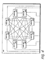
- FIG. 4 illustrates one embodiment of a logic board suitable for distributively packaging the above described logic chips to form scalable emulator 14 in accordance with the scaling teachings of the present invention.
- each logic board 200 includes a number of logic chips 100 described earlier.
- logic chips 100 of the same logic board 200 are directly and fully interconnected with one another, to provide deterministic timing delay within the logic board for emulation signal routing between the logic chips 100 of the same logic board 200.
- Each "direct connection" includes multiple direction connections between I/O pins of two logic chips 100. The number of direct connections provided between any two logic chips is application dependent, depending on the number of I/O pins available per logic chip, and the number of logic chips included in each logic board.
- Mapping software 22 when interconnecting allocated logic resources further advantageously leverages on the fully interconnected architecture of logic board 200 and confines all inter-logic chip emulation signal routing between logic chips 100 of logic board 200 to the direct connections between them.
- other board level interconnect architecture e.g. a partial interconnect or a nearest neighbor interconnect architecture, may be employed for logic board 200 instead.
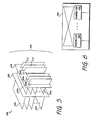
- Figure 5 illustrates a basic embodiment of scalable emulator 14.
- basic embodiment of emulator 14 is formed with emulation resources inter-coupled and physically disposed in half of a crate; more specifically, in the top half of crate 300 .
- Logic boards 200 are horizontally disposed.
- Logic chips 100 of logic boards 200 are reconfigurably interconnected together by interconnect chips (not shown) of interconnect boards 204a and 204b.
- Interconnect boards 204a are correspondingly coupled to logic boards 200 through connectors (not shown) disposed on backplane 206.
- Interconnect boards 204b in turn are orthogonally interconnected to interconnect boards 204a through connectors (not shown) disposed on backplane 208.
- I/O and service boards 210 and 212 are also orgthogonally interconnected to interconnect boards 204a as shown.
- interconnect boards 204b includes in particular expansion connectors (not shown) for facilitating scaling of emulator 14 in one or more selected ones of a number of scaling orientations through coupling of one or more substantial replicates of basic embodiment 302 to basic embodiment 302.
- FIG. 6 illustrates a generic embodiment of an interconnect board 204.
- each interconnect board 204 includes a number of emulation signal routing chip 306.
- Interconnect boards 204a and 204b of Figure 5 differ from each other only in terms of the number routing chips 306 included, and the manner the routing chips 306 are wired to the I/O pins (not shown) of the interconnect board 204a or 204b .
- identical interconnect boards i.e. with same number of routing chips and same chip to pin wiring pattern, may be employed.
- “hybrid" interconnect boards i.e. boards with logic as well as interconnect chips, may also be employed instead.
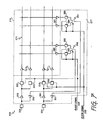
- FIG. 7 illustrates one embodiment of a routing chip suitable for use in interconnect board 204.
- routing chip 320 is of a multi-clocked type.
- routing chip 320 includes a "static" portion 376 and a "dynamic" portion 377 (the rest of routing chip 320 ).
- Static portion 376 includes grid 375 , drivers 370 and 371 , and drivers 380 and 381 .
- Dynamic portion 377 includes a number of I/O pins. For ease of illustration, only two I/O pins 333 and 334 are shown. Additionally, dynamic portion 377 includes drivers 360, 361, 365 and 367, latches 355, 356, 385 and 386, and switches 390 and 391.
- Static portion 376 is not clocked, whereas dynamic portion 377 Is controlled by a number of clock signals.
- two clock signals 349 and 350 are shown. Together, these elements enable emulation signal to be reconfigurably routed in multiple regional time domains.
- other routing chips including "hybrid" routing chips with logic functions, such as conventional FPGA may be employed instead.
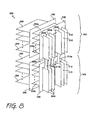
- Figure 8 illustrates a first expanded embodiment of emulator 14 in accordance with the scaling teachings of the present invention.
- emulator 14 is formed with basic embodiment 302 described earlier, and a substantial replicate 304 of basic embodiment 302, with basic embodiment 302 disposed at the top half of crate 300 and substantial replicate 304 disposed at the bottom half of crate 300.
- substantial replicate 304 is the same as basic embodiment 302 except for interconnect boards 204d, which differ from interconnect boards 204b in that each of Interconnect boards 204d for convenience purpose, contains wiring traces only and no routing chips nor expansion connectors. Otherwise the rest of the emulation resources are the same, including interconnect boards 204c, which are identical to interconnect boards 204a.
- dissimilar number of logic boards as well as dissimilar logic boards may be employed.
- dissimilar backplanes may also be employed.
- keeping scaling replicate 304 substantially similar to basic embodiment 302 has the advantage of keeping the half crate and full crate embodiments transparent to the circuit design partitioner of mapping software 22.
- keep the top half and the bottom half of emulator 14 substantially symmetric has the advantage of making it easier for the emulation resources to be shared by, multiple circuit designs being "concurrently" emulated. Sharing emulation resources implies concurrent emulation of multiple circuit designs.
- interconnect boards 204b and 204d are interconnected using flex PCBs 214a.
- Each flex PCB 214a includes a number of wiring traces connecting I/O pins at one end to I/O pins at the other end of flex PCB 214a.
- Flex PCBs 214a advantageously provide a reliable way of interconnecting the two collections of emulation resources, but yet provide the flexibility of allowing for manufacturing misalignment between interconnect boards 204b of basic embodiment 302 and interconnect boards 204d of replicate 304.
- FIG. 9 illustrates a second expanded embodiment of scalable emulator 14 in accordance with the scaling teachings of the present invention.
- scalable emulator 14 is formed with two crates 300 in a back-to-back manner (or side-by-side, with the two crates rotated 90 degrees), using interconnect resources packed in interconnect crate 400.
- the emulation resources of the two crates 300 are substantially identical.
- crates with dissimilar emulation resources may be employed.
- keeping the emulation resources of the two crates 300 substantially similar to one another has the advantage of keeping the single crate and double crate embodiments transparent to the circuit design partitioner of mapping software 22.
- keeping the emulation resources of the two crates of scalable emulator 14 substantially symmetric has the advantage of making it easier for the emulation resources to be shared by multiple circuit designs being "concurrently" emulated.
- interconnect crate 400 includes interconnect boards 204e and 204f and backplane 208.
- interconnect boards 204e differ from interconnect boards 204a and 204b, but interconnect boards 204f are identical to interconnect boards 204b.
- identical interconnect boards or totally dissimilar interconnect boards may be employed.
- keeping the interconnect boards substantially similar has the advantage of keeping the single crate and double crate embodiments transparent to the circuit design partitioner of mapping software 22.
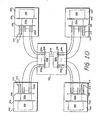
- FIG 10 illustrates a third expanded embodiment of scalable emulator 14 in accordance with the scaling teachings of the present invention.
- scalable emulator 14 is formed with four crates 300 in a quad manner, using interconnect resources packed in interconnect crate 400.
- the emulation resources of the four crates 300 are substantially identical.
- crates with dissimilar emulation resources may be employed.
- keeping the emulation resources of the four crates 300 substantially similar to one another has the advantage of keeping the two crate and four crate embodiments transparent to the circuit design partitioner of mapping software 22.
- keeping the emulation resources of the four crates of scalable emulator 14 substantially symmetric has the advantage of making it easier for the emulation resources to be shared by two or more circuit designs being "concurrently" emulated.
- interconnect crate 400 includes interconnect boards 204e, 204f and 204g, and backplanes 208.
- interconnect boards 204e differ from interconnect boards 204a and 204b, but interconnect boards 204f and 204g are identical to interconnect boards 204b and 204d described earlier.
- identical interconnect boards or totally dissimilar interconnect boards may be employed, with advantages and disadvantages as set forth before.
- the present invention has been described in terms of the above illustrated embodiments, those skilled in the art will recognize that the invention is not limited to the embodiments described.
- the scaling may extend beyond 8x scaling (from half crate to 4 crate) illustrated, with additional granularity.
- the scaling may be advantageously effectuated with the transparency to the circuit design partitioning software, and the symmetry of the emulation resources maintained. Accordingly, the present invention can be practiced with modification and alteration within the and scope of the appended claims. The description is thus to be regarded as illustrative instead of restrictive on the present invention.
Landscapes
- Engineering & Computer Science (AREA)
- Computer Hardware Design (AREA)
- Physics & Mathematics (AREA)
- Theoretical Computer Science (AREA)
- Evolutionary Computation (AREA)
- Geometry (AREA)
- General Engineering & Computer Science (AREA)
- General Physics & Mathematics (AREA)
- Test And Diagnosis Of Digital Computers (AREA)
- Image Processing (AREA)
- Medicines Containing Antibodies Or Antigens For Use As Internal Diagnostic Agents (AREA)
Abstract
Description
Claims (27)
- An emulation system comprising(a) a first plurality of reconfigurable logic boards (200); and(b) a first plurality of reconfigurable interconnect boards (204a) correspondingly coupled to the first plurality of logic boards (200), and a second plurality of interconnect boards (204b) orthogonally coupled to the first plurality of interconnect boards (204a), each of the second plurality of interconnect boards (204b) further including a first plurality of expansion connectors for facilitating expansion of the emulation system in one or more selected ones of expansion orientations.
- The emulation system of claim 1, wherein each logic board (200) includes a first plurality of logic chips (100) reconfigurable to emulate a first plurality of circuit elements of a circuit design, each of the first plurality of interconnect boards (204a) includes a first plurality of interconnect chips (306), each of the second plurality of interconnect boards (204b) includes a second plurality of interconnect chips (306), and the first and second plurality of interconnect chips of each of the first and second plurality of interconnect boards are reconfigurable to selectively interconnect the logic chips of different ones of the first plurality of logic boards (200).
- The emulation system of claim 2, wherein the emulation system further comprises:(c) a second plurality of logic boards (200), wherein each logic board includes a second plurality of logic chips (100) reconfigurable to emulate a second plurality of circuit elements of the circuit design; and(d) a third plurality of interconnect boards (204c) correspondingly coupled to the second plurality of logic boards (200), and a fourth plurality of interconnect boards (204d) orthogonally coupled to the third plurality of interconnect boards (204c) and correspondingly coupled to the second plurality of interconnect boards (204b) through selected ones of the first plurality of expansion connectors of each of the second plurality of interconnect boards (204b), wherein each of the third plurality of interconnect boards (204c) includes a third plurality of interconnect chips (306), and wherein the third plurality of interconnect chips of each of the third plurality of interconnect boards (204c) are reconfigurable to cooperate with the first and second plurality of interconnect chips of each of the first and second plurality of interconnect boards (204a, 204b) to selectively interconnect the logic chips of different ones of the first and second plurality of logic boards.
- The emulation system of claim 3, wherein each of the fourth plurality of interconnect boards (204d) further comprises a second plurality of expansion connectors, and the emulation system further comprises a first plurality of flex printed circuit boards (PCBs) (214a) correspondingly coupling selected ones of the first plurality of expansion connectors of each of the second plurality of interconnect boards (204b) to selected ones of the second plurality of expansion connectors of each of the fourth plurality of interconnect boards (204d).
- The emulation system of claim 3, wherein the first and second plurality of logic boards, and the first, second, third and fourth interconnect boards are packaged in a single cabinet with the first plurality of logic boards and the first and second interconnect boards (204a, 204b) occupying an upper portion of the cabinet, and the second plurality of logic boards and the third and fourth interconnect boards (204c, 204d) occupying a lower portion of the cabinet.
- The emulation system of claim 3, wherein each of the fourth plurality of interconnect boards (204d) includes a fourth plurality of interconnect chips (306), and wherein the fourth plurality of interconnect chips of each of the fourth plurality of interconnect boards (204d) are also reconfigurable to cooperate with the first, second and third interconnect chips of each of the first, second and third plurality of interconnect boards (204a, 204b, 204c) to selectively interconnect the logic chips of different ones of the first and second plurality of logic boards (200).
- The emulation system of claim 6, wherein the first and second plurality of logic boards (200), and the first, second, third and fourth interconnect boards (204a, 204b, 204c, 204d) are packaged in a single cabinet with the first plurality of logic boards and the first and second interconnect boards occupying an upper portion of the cabinet, and the second plurality of logic boards and the third and fourth interconnect boards occupying a lower portion of the cabinet.
- The emulation system of claim 6, wherein the emulation system further comprises:(e) a fifth and a sixth plurality of interconnect boards (204e) correspondingly coupled to the second and fourth plurality of interconnect boards (204b, 204d) through the first and second plurality of expansion connectors of each of the second and fourth plurality of interconnect boards, and a seventh plurality of interconnect boards (204f) orthogonally coupled to the fifth and sixth plurality of interconnect boards (204e), wherein each of the fifth, sixth and seventh plurality of interconnect boards includes a fifth, sixth and seventh plurality of interconnect chips, and wherein the fifth, sixth and seventh plurality of interconnect chips of each of the fifth, sixth and seventh plurality of interconnect boards are reconfigurable to cooperate with the first, second third and fourth plurality of interconnect chips of each of the first, second, third and fourth plurality of the interconnect boards to selectively interconnect the logic chips of different ones of the first and second plurality of logic boards.
- The emulation system of claim 8, wherein the first and second plurality of logic boards, and the first, second, third, fourth, fifth, sixth and seventh interconnect boards are packaged in three cabinets with the first plurality of logic boards and the first and second interconnect boards occupying a first cabinet (300), the second plurality of logic boards and the third and fourth interconnect boards occupying a second cabinet (300), and the fifth, sixth and seventh interconnect boards occupying a third cabinet (400).
- The emulation system of claim 6, wherein the emulation system further comprises:(e) a fifth and a sixth plurality of interconnect boards (204e) correspondingly coupled to the second and fourth plurality of interconnect boards (204b) through the first and second plurality of expansion connectors of each of the second and fourth plurality of interconnect boards, a seventh and an eighth plurality of interconnect boards (204f) correspondingly coupled to each other and orthogonally coupled to the fifth and sixth plurality of interconnect boards (204e) respectively, wherein each of the fifth, sixth and seventh plurality of interconnect boards includes a fifth, sixth and seventh plurality of interconnect chips, and wherein the fifth, sixth and seventh plurality of interconnect chips of each of the fifth, sixth and seventh plurality of interconnect boards are reconfigurable to cooperate with the first, second, third and fourth plurality of interconnect boards to selectively interconnect the logic chips of different ones of the first and second plurality of logic boards.
- The emulation system of claim 10, wherein the first and second plurality of logic boards, and the first, second, third, fourth, fifth, sixth, seventh and eighth interconnect boards are packaged in three cabinets with the first plurality of logic boards and the first and second interconnect boards occupying a first cabinet (300), the second plurality of logic boards and the third and fourth interconnect boards occupying a second cabinet (300), and the fifth, sixth and seventh interconnect boards occupying a third cabinet (400).
- The emulation system of claim 10, wherein each of the seventh plurality of interconnect boards (204f) includes a third plurality of expansion connectors,
each of the eighth plurality of interconnect boards (204f) includes a fourth plurality of expansion connectors, and
the emulation system further comprises a plurality of flex printed circuit boards (214b) correspondingly coupling the third plurality of expansion connectors of each of the seventh plurality of interconnect boards to the fourth plurality of expansion connectors of each of the eighth plurality of interconnect boards. - The emulation system of claim 10, wherein each of the eighth plurality of interconnect boards (204f) includes an eighth plurality of interconnect chips, and wherein the eighth plurality of interconnect chips of each of the eighth plurality of interconnect boards are also reconfigurable to cooperate with the first, second, third, fourth, fifth, sixth and seventh interconnect chips of each of the first, second, third, fourth, fifth, sixth and seventh interconnect boards to selectively interconnect the logic chips of different ones of the first and second plurality of logic boards.
- The emulation system of claim 1, wherein the emulation system further comprises
(c) a second plurality of logic boards (200), a third plurality of interconnect boards (204c) correspondingly coupled to the second plurality of logic boards (200), and a fourth plurality of interconnect boards (204d) orthogonally coupled to the third plurality of interconnect boards (204c) and correspondingly coupled to the second plurality of interconnect boards (204b) through selected ones of the first plurality of expansion connectors of each of the second plurality of interconnect boards (204b). - The emulation system of claim 14, wherein each of the fourth plurality of interconnect boards (204d) further comprises a second plurality of expansion connectors, and the emulation system further comprises a first plurality of flex printed circuit boards (PCBs) (214a) correspondingly coupling selected ones of the first plurality of expansion connectors of each of the second plurality of interconnect boards (204b) to selected ones of the second plurality of expansion connectors of each of the fourth plurality of interconnect boards (204d).
- The emulation system of claim 14, wherein the first and second plurality of logic boards (200), and the first, second, third and fourth interconnect boards (204a, 204b, 204c, 204d) are packaged in a single cabinet with the first plurality of logic boards (200) and the first and second interconnect boards (204a, 204b) occupying an upper portion of the cabinet, and the second plurality of logic boards (200) and the third and fourth interconnect boards (204c, 204d) occupying a lower portion of the cabinet.
- The emulation system of claim 14, wherein the emulation system further comprises
(d) a fifth and a sixth plurality of interconnect boards (204e) correspondingly coupled to the second and fourth plurality of interconnect boards through the first and second plurality of expansion connectors of each of the second and fourth plurality of interconnect boards, and a seventh plurality of interconnect boards (204f) orthogonally coupled to the fifth and sixth plurality of interconnect boards. - The emulation system of claim 17, wherein the first and second plurality of logic boards, and the first, second, third, fourth, fifth, sixth and seventh interconnect boards are packaged in three cabinets with the first plurality of logic boards and the first and second interconnect boards occupying a first cabinet (300), the second plurality of logic boards and the third and fourth interconnect boards occupying a second cabinet (300), and the fifth, sixth and seventh interconnect boards occupying a third cabinet (400).
- The emulation system of claim 14, wherein the emulation system further comprises
(d) a fifth and a sixth plurality of interconnect boards correspondingly coupled to the second and fourth plurality of interconnect boards through the first and second plurality of expansion connectors of each of the second and fourth plurality of interconnect boards, a seventh and an eighth plurality of interconnect boards correspondingly coupled to each other and orthogonally coupled to the fifth and sixth plurality of interconnect boards respectively. - The emulation system of claim 19, wherein the first and second plurality of logic boards, and the first, second, third, fourth, fifth, sixth, seventh and eighth interconnect boards are packaged in three cabinets with the first plurality of logic boards and the first and second interconnect boards occupying a first cabinet, the second plurality of logic boards and the third and fourth interconnect boards occupying a second cabinet, and the fifth, sixth and seventh interconnect boards occupying a third cabinet.
- The emulation system of claim 19, wherein
each of the seventh plurality of interconnect boards includes a third plurality of expansion connectors,
each of the eighth plurality of interconnect boards includes a fourth plurality of expansion connectors, and
the emulation system further comprises a plurality of flex printed circuit boards (PCBs) (214b) correspondingly coupling the third plurality of expansion connectors of each of the seventh plurality of interconnect boards (204f) to the fourth plurality of expansion connectors of each of the eighth plurality of interconnect boards (204f). - The emulation system of claim 14, wherein each of the fourth plurality of interconnect boards (204d) also has a second plurality of expansion connectors; and further comprising
(d) a first plurality of flex printed circuit boards (214a) correspondingly coupling selected ones of the first plurality of expansion connectors of each of the second plurality of interconnect boards (204b) to selected ones of the second plurality of expansion connectors of each of the fourth plurality of interconnect boards (204d). - The emulation system of claim 22, wherein the first and second plurality of logic boards, and the first, second, third and fourth interconnect boards are packaged in a single cabinet with the first plurality of logic boards and the first and second interconnect boards occupying an upper portion of the cabinet, and the second plurality of logic boards and the third and fourth interconnect boards occupying a lower portion of the cabinet.
- The emulation system of claim 22, wherein the emulation system further comprises
(d) a fifth and a sixth plurality of interconnect boards correspondingly coupled to the second and fourth plurality of logic boards through the first and second plurality of expansion connectors of each of the second and fourth plurality of logic boards, and a seventh plurality of interconnect boards (204f) orthogonally coupled to the fifth and sixth plurality of interconnect boards (204e). - The emulation system of claim 24, wherein the first and second plurality of logic boards, and the first, second, third, fourth, fifth, sixth and seventh interconnect boards are packaged in three cabinets with the first plurality of logic boards, and the first and second interconnect boards occupying a first cabinet (300), the second plurality of logic boards and the third and fourth interconnect boards occupying a second cabinet (300), and the fifth, sixth and seventh interconnect boards occupying a third cabinet (400).
- The emulation system of claim 22, wherein the emulation system further comprises
(d) a fifth and a sixth plurality of interconnect boards (204e) correspondingly coupled to the second and fourth plurality of interconnect boards through the first and second plurality of expansion connectors of each of the second and fourth plurality of interconnect boards, a seventh and an eighth plurality of interconnect boards (204f) correspondingly coupled to each other and orthogonally coupled to the fifth and sixth plurality of interconnect boards (204e) respectively. - The emulation system of claim 26, wherein the first and second plurality of logic boards, and the first, second, third, fourth, fifth, sixth, seventh and eighth interconnect boards are packaged in three cabinets with the first plurality of logic boards and the first and second interconnect boards occupying a first cabinet (300), the second plurality of logic boards and the third and fourth interconnect boards occupying a second cabinet (300), and the fifth, sixth and seventh interconnect boards occupying a third cabinet (400).
Applications Claiming Priority (3)
| Application Number | Priority Date | Filing Date | Title |
|---|---|---|---|
| US09/405,602 US6647362B1 (en) | 1999-09-24 | 1999-09-24 | Emulation system scaling |
| US405602 | 1999-09-24 | ||
| PCT/US2000/003111 WO2001024369A1 (en) | 1999-09-24 | 2000-02-04 | Emulation system scaling |
Publications (2)
| Publication Number | Publication Date |
|---|---|
| EP1114513A1 EP1114513A1 (en) | 2001-07-11 |
| EP1114513B1 true EP1114513B1 (en) | 2003-05-07 |
Family
ID=23604375
Family Applications (1)
| Application Number | Title | Priority Date | Filing Date |
|---|---|---|---|
| EP00910094A Expired - Lifetime EP1114513B1 (en) | 1999-09-24 | 2000-02-04 | Emulation system scaling |
Country Status (7)
| Country | Link |
|---|---|
| US (1) | US6647362B1 (en) |
| EP (1) | EP1114513B1 (en) |
| JP (1) | JP3594557B2 (en) |
| AT (1) | ATE240008T1 (en) |
| AU (1) | AU3224200A (en) |
| DE (1) | DE60002550T2 (en) |
| WO (1) | WO2001024369A1 (en) |
Families Citing this family (6)
| Publication number | Priority date | Publication date | Assignee | Title |
|---|---|---|---|---|
| US20030229612A1 (en) * | 2002-06-10 | 2003-12-11 | Keller S. Brandon | Circuit design duplication system |
| EP1726073A4 (en) | 2003-11-28 | 2008-12-17 | Kenneth James Warburton | Bridged parallel distributing frame |
| US7698118B2 (en) * | 2004-04-15 | 2010-04-13 | Mentor Graphics Corporation | Logic design modeling and interconnection |
| US7379861B2 (en) * | 2004-05-28 | 2008-05-27 | Quickturn Design Systems, Inc. | Dynamic programming of trigger conditions in hardware emulation systems |
| TWI450118B (en) * | 2010-11-02 | 2014-08-21 | Global Unichip Corp | Hybrid electronic design system and reconfigurable connection matrix thereof |
| WO2017139867A1 (en) | 2016-02-16 | 2017-08-24 | Développement Effenco Inc. | Expanded functionlity stop-start fuel saving system for vocational vehicles |
Family Cites Families (11)
| Publication number | Priority date | Publication date | Assignee | Title |
|---|---|---|---|---|
| US4914612A (en) | 1988-03-31 | 1990-04-03 | International Business Machines Corporation | Massively distributed simulation engine |
| EP0437491B1 (en) | 1988-10-05 | 1995-12-13 | Quickturn Systems Inc | Method of using electronically reconfigurable gate array logic and apparatus formed thereby |
| US5282271A (en) | 1991-10-30 | 1994-01-25 | I-Cube Design Systems, Inc. | I/O buffering system to a programmable switching apparatus |
| US5352123A (en) | 1992-06-08 | 1994-10-04 | Quickturn Systems, Incorporated | Switching midplane and interconnection system for interconnecting large numbers of signals |
| US5424589A (en) | 1993-02-12 | 1995-06-13 | The Board Of Trustees Of The Leland Stanford Junior University | Electrically programmable inter-chip interconnect architecture |
| US5682107A (en) | 1994-04-01 | 1997-10-28 | Xilinx, Inc. | FPGA architecture with repeatable tiles including routing matrices and logic matrices |
| US5604888A (en) | 1994-04-07 | 1997-02-18 | Zycad Corporation | Emulation system employing motherboard and flexible daughterboards |
| US5838908A (en) * | 1994-11-14 | 1998-11-17 | Texas Instruments Incorporated | Device for having processors each having interface for transferring delivery units specifying direction and distance and operable to emulate plurality of field programmable gate arrays |
| US5574388A (en) | 1995-10-13 | 1996-11-12 | Mentor Graphics Corporation | Emulation system having a scalable multi-level multi-stage programmable interconnect network |
| US5907697A (en) | 1995-10-13 | 1999-05-25 | Mentor Graphics Corporation | Emulation system having a scalable multi-level multi-stage hybrid programmable interconnect network |
| US5903744A (en) | 1997-05-15 | 1999-05-11 | Logic Express System, Inc. | Logic emulator using a disposable wire-wrap interconnect board with an FPGA emulation board |
-
1999
- 1999-09-24 US US09/405,602 patent/US6647362B1/en not_active Expired - Lifetime
-
2000
- 2000-02-04 WO PCT/US2000/003111 patent/WO2001024369A1/en not_active Ceased
- 2000-02-04 AT AT00910094T patent/ATE240008T1/en not_active IP Right Cessation
- 2000-02-04 JP JP2000602888A patent/JP3594557B2/en not_active Expired - Fee Related
- 2000-02-04 DE DE60002550T patent/DE60002550T2/en not_active Expired - Lifetime
- 2000-02-04 EP EP00910094A patent/EP1114513B1/en not_active Expired - Lifetime
- 2000-02-04 AU AU32242/00A patent/AU3224200A/en not_active Abandoned
Also Published As
| Publication number | Publication date |
|---|---|
| US6647362B1 (en) | 2003-11-11 |
| DE60002550T2 (en) | 2004-03-18 |
| WO2001024369A1 (en) | 2001-04-05 |
| ATE240008T1 (en) | 2003-05-15 |
| EP1114513A1 (en) | 2001-07-11 |
| JP3594557B2 (en) | 2004-12-02 |
| AU3224200A (en) | 2001-04-30 |
| DE60002550D1 (en) | 2003-06-12 |
| JP2002538539A (en) | 2002-11-12 |
Similar Documents
| Publication | Publication Date | Title |
|---|---|---|
| Beckhoff et al. | The xilinx design language (xdl): Tutorial and use cases | |
| US5535342A (en) | Pld connector for module having configuration of either first PLD or second PLD and reconfigurable bus for communication of two different bus protocols | |
| US4914612A (en) | Massively distributed simulation engine | |
| JP2989518B2 (en) | Multi-processor emulation system | |
| US7856545B2 (en) | FPGA co-processor for accelerated computation | |
| US5603043A (en) | System for compiling algorithmic language source code for implementation in programmable hardware | |
| JP3162687B2 (en) | Method of constructing logic configuration using electrically reconfigurable gate array | |
| US7739097B2 (en) | Emulation system with time-multiplexed interconnect | |
| US20020177990A1 (en) | Distributed logic analyzer for use in a hardware logic emulation system | |
| KR19990077413A (en) | Emulation module having planar array organization | |
| US7821849B2 (en) | Configurable embedded processor | |
| CA2148814A1 (en) | Video processing hardware | |
| JP2002358340A (en) | Circuit used for logic emulation, logic board having the circuit, logic emulator, and communication method in logic emulation | |
| US7184946B2 (en) | Co-simulation via boundary scan interface | |
| JP3592639B2 (en) | Time multiplex emulation system in the area | |
| US6675364B1 (en) | Insertion of scan hardware | |
| US6647362B1 (en) | Emulation system scaling | |
| Khan et al. | FPGA architectures for ASIC hardware emulators | |
| Bainbridge et al. | The design and test of a smartcard chip using a CHAIN self-timed network-on-chip | |
| US5622770A (en) | Printed circuit board design utilizing flexible interconnects for programmable logic components | |
| US5546566A (en) | Emulation system for microcomputer | |
| US20020091507A1 (en) | Logic emulator with routing chip providing virtual full-crossbar interconnect | |
| US20040254778A1 (en) | Reconfigurable logic element with input swapping | |
| Davis | Synthesizing asynchronous circuits: Practice and experience | |
| Rincon et al. | Core+ ASIC methodology: the pursuit of system-on-a-chip |
Legal Events
| Date | Code | Title | Description |
|---|---|---|---|
| PUAI | Public reference made under article 153(3) epc to a published international application that has entered the european phase |
Free format text: ORIGINAL CODE: 0009012 |
|
| 17P | Request for examination filed |
Effective date: 20000822 |
|
| AK | Designated contracting states |
Kind code of ref document: A1 Designated state(s): AT BE CH CY DE DK ES FI FR GB GR IE IT LI LU MC NL PT SE |
|
| 17Q | First examination report despatched |
Effective date: 20010706 |
|
| GRAH | Despatch of communication of intention to grant a patent |
Free format text: ORIGINAL CODE: EPIDOS IGRA |
|
| RIN1 | Information on inventor provided before grant (corrected) |
Inventor name: LEPAPE, OLIVIER Inventor name: REBLEWSKI, FREDERIC Inventor name: BARBIER, JEAN |
|
| GRAH | Despatch of communication of intention to grant a patent |
Free format text: ORIGINAL CODE: EPIDOS IGRA |
|
| GRAA | (expected) grant |
Free format text: ORIGINAL CODE: 0009210 |
|
| AK | Designated contracting states |
Designated state(s): AT BE CH CY DE DK ES FI FR GB GR IE IT LI LU MC NL PT SE |
|
| PG25 | Lapsed in a contracting state [announced via postgrant information from national office to epo] |
Ref country code: IT Free format text: LAPSE BECAUSE OF FAILURE TO SUBMIT A TRANSLATION OF THE DESCRIPTION OR TO PAY THE FEE WITHIN THE PRESCRIBED TIME-LIMIT;WARNING: LAPSES OF ITALIAN PATENTS WITH EFFECTIVE DATE BEFORE 2007 MAY HAVE OCCURRED AT ANY TIME BEFORE 2007. THE CORRECT EFFECTIVE DATE MAY BE DIFFERENT FROM THE ONE RECORDED. Effective date: 20030507 Ref country code: CY Free format text: LAPSE BECAUSE OF FAILURE TO SUBMIT A TRANSLATION OF THE DESCRIPTION OR TO PAY THE FEE WITHIN THE PRESCRIBED TIME-LIMIT Effective date: 20030507 Ref country code: CH Free format text: LAPSE BECAUSE OF FAILURE TO SUBMIT A TRANSLATION OF THE DESCRIPTION OR TO PAY THE FEE WITHIN THE PRESCRIBED TIME-LIMIT Effective date: 20030507 Ref country code: NL Free format text: LAPSE BECAUSE OF FAILURE TO SUBMIT A TRANSLATION OF THE DESCRIPTION OR TO PAY THE FEE WITHIN THE PRESCRIBED TIME-LIMIT Effective date: 20030507 Ref country code: FI Free format text: LAPSE BECAUSE OF FAILURE TO SUBMIT A TRANSLATION OF THE DESCRIPTION OR TO PAY THE FEE WITHIN THE PRESCRIBED TIME-LIMIT Effective date: 20030507 Ref country code: AT Free format text: LAPSE BECAUSE OF FAILURE TO SUBMIT A TRANSLATION OF THE DESCRIPTION OR TO PAY THE FEE WITHIN THE PRESCRIBED TIME-LIMIT Effective date: 20030507 Ref country code: BE Free format text: LAPSE BECAUSE OF FAILURE TO SUBMIT A TRANSLATION OF THE DESCRIPTION OR TO PAY THE FEE WITHIN THE PRESCRIBED TIME-LIMIT Effective date: 20030507 Ref country code: LI Free format text: LAPSE BECAUSE OF FAILURE TO SUBMIT A TRANSLATION OF THE DESCRIPTION OR TO PAY THE FEE WITHIN THE PRESCRIBED TIME-LIMIT Effective date: 20030507 |
|
| REG | Reference to a national code |
Ref country code: GB Ref legal event code: FG4D |
|
| REG | Reference to a national code |
Ref country code: CH Ref legal event code: EP |
|
| REG | Reference to a national code |
Ref country code: IE Ref legal event code: FG4D |
|
| REF | Corresponds to: |
Ref document number: 60002550 Country of ref document: DE Date of ref document: 20030612 Kind code of ref document: P |
|
| PG25 | Lapsed in a contracting state [announced via postgrant information from national office to epo] |
Ref country code: DK Free format text: LAPSE BECAUSE OF FAILURE TO SUBMIT A TRANSLATION OF THE DESCRIPTION OR TO PAY THE FEE WITHIN THE PRESCRIBED TIME-LIMIT Effective date: 20030807 Ref country code: GR Free format text: LAPSE BECAUSE OF FAILURE TO SUBMIT A TRANSLATION OF THE DESCRIPTION OR TO PAY THE FEE WITHIN THE PRESCRIBED TIME-LIMIT Effective date: 20030807 Ref country code: SE Free format text: LAPSE BECAUSE OF FAILURE TO SUBMIT A TRANSLATION OF THE DESCRIPTION OR TO PAY THE FEE WITHIN THE PRESCRIBED TIME-LIMIT Effective date: 20030807 Ref country code: PT Free format text: LAPSE BECAUSE OF FAILURE TO SUBMIT A TRANSLATION OF THE DESCRIPTION OR TO PAY THE FEE WITHIN THE PRESCRIBED TIME-LIMIT Effective date: 20030807 |
|
| PG25 | Lapsed in a contracting state [announced via postgrant information from national office to epo] |
Ref country code: ES Free format text: LAPSE BECAUSE OF FAILURE TO SUBMIT A TRANSLATION OF THE DESCRIPTION OR TO PAY THE FEE WITHIN THE PRESCRIBED TIME-LIMIT Effective date: 20030818 |
|
| NLV1 | Nl: lapsed or annulled due to failure to fulfill the requirements of art. 29p and 29m of the patents act | ||
| REG | Reference to a national code |
Ref country code: CH Ref legal event code: PL |
|
| PG25 | Lapsed in a contracting state [announced via postgrant information from national office to epo] |
Ref country code: LU Free format text: LAPSE BECAUSE OF NON-PAYMENT OF DUE FEES Effective date: 20040204 Ref country code: IE Free format text: LAPSE BECAUSE OF NON-PAYMENT OF DUE FEES Effective date: 20040204 Ref country code: GB Free format text: LAPSE BECAUSE OF NON-PAYMENT OF DUE FEES Effective date: 20040204 |
|
| PG25 | Lapsed in a contracting state [announced via postgrant information from national office to epo] |
Ref country code: MC Free format text: LAPSE BECAUSE OF NON-PAYMENT OF DUE FEES Effective date: 20040228 |
|
| ET | Fr: translation filed | ||
| PLBE | No opposition filed within time limit |
Free format text: ORIGINAL CODE: 0009261 |
|
| STAA | Information on the status of an ep patent application or granted ep patent |
Free format text: STATUS: NO OPPOSITION FILED WITHIN TIME LIMIT |
|
| 26N | No opposition filed |
Effective date: 20040210 |
|
| GBPC | Gb: european patent ceased through non-payment of renewal fee |
Effective date: 20040204 |
|
| REG | Reference to a national code |
Ref country code: IE Ref legal event code: MM4A |
|
| REG | Reference to a national code |
Ref country code: FR Ref legal event code: PLFP Year of fee payment: 17 |
|
| REG | Reference to a national code |
Ref country code: FR Ref legal event code: PLFP Year of fee payment: 18 |
|
| REG | Reference to a national code |
Ref country code: FR Ref legal event code: PLFP Year of fee payment: 19 |
|
| PGFP | Annual fee paid to national office [announced via postgrant information from national office to epo] |
Ref country code: FR Payment date: 20171220 Year of fee payment: 19 |
|
| REG | Reference to a national code |
Ref country code: DE Ref legal event code: R082 Ref document number: 60002550 Country of ref document: DE Representative=s name: MAIER, DANIEL OLIVER, DIPL.-ING. UNIV., DE |
|
| PGFP | Annual fee paid to national office [announced via postgrant information from national office to epo] |
Ref country code: DE Payment date: 20171221 Year of fee payment: 19 |
|
| REG | Reference to a national code |
Ref country code: DE Ref legal event code: R119 Ref document number: 60002550 Country of ref document: DE |
|
| PG25 | Lapsed in a contracting state [announced via postgrant information from national office to epo] |
Ref country code: DE Free format text: LAPSE BECAUSE OF NON-PAYMENT OF DUE FEES Effective date: 20190903 |
|
| PG25 | Lapsed in a contracting state [announced via postgrant information from national office to epo] |
Ref country code: FR Free format text: LAPSE BECAUSE OF NON-PAYMENT OF DUE FEES Effective date: 20190228 |