The present invention relates to digital processor devices,
and more particularly, but not exclusively, to monitoring the
operation and performance of digital microprocessors.
Microprocessors are general purpose processors which
require high instruction throughputs in order to execute
software running thereon, and can have a wide range of
processing requirements depending on the particular software
applications involved. Microprocessors are now combined with
memory circuits and other peripheral circuits into a single
integrated circuit and may be custom designed for a particular
target system. Often, access to a microprocessor in a target
system for software development and debugging is difficult.
Known microprocessor debugging environments provide a means
for gaining access to a microprocessor in a target system, of
which In Circuit Emulation (ICE) is a commonly favored
technique. Typically, a processor in the target system is
temporarily replaced by an emulation module that provides
connectivity to a test system for monitoring and modifying
target system software that is executed by the emulation module.
Alternatively, the target processor is connected to the
test system via a test access port, such a JTAG, and the target
processor executes the target system software while exchanging
test information with the test system via the test access port.
JTAG is defined in IEEE 1149.1 - 1990 "Standard Test Access Port
and Boundary Scan Architecture. Terms and concepts relating to
IEEE 1149.1 which are used herein, are explained fully in this
IEEE standard. The IEEE 1149.1 standard provides a
communication protocol that allows the selection of one or more
devices imbedded within a system. This protocol implements the
primitives necessary to control on-chip debug and test
facilities.
Many different types of processors are known, of which
microprocessors are but one example. For example, Digital
Signal Processors (DSPs) are widely used, in particular for
specific applications, such as mobile processing applications.
DSPs are typically configured to optimize the performance of the
applications concerned and to achieve this they employ more
specialized execution units and instruction sets. Particularly
in, but not exclusively, applications such as disk controllers
for portable computers and mobile telecommunications, it is
desirable to provide ever increasing DSP performance while
keeping power consumption as low as possible.
A method and apparatus has now been developed for emulating
a block of memory in a target system with two or more blocks of
memory that operate in lock step. Particular and preferred
aspects of the invention are set out in the accompanying
independent and dependent claims.
In accordance with a first aspect of the invention, there
is provided a digital system that has a memory block. The
memory block has an address bus for receiving an address, the
address decoding circuitry is connected to the address bus. The
address decoding circuitry is operable to detect if a received
address is within a preselected address block. Bank decode
circuitry is connected to the address bus and is operable to
detect if a received address is within a preselected address
bank. Memory circuitry is connected to the address bus and is
operable to transfer data on a data bus in response to a
received address if the received address is within the
preselected bank and the preselected address block. Control
circuitry is connected to the address decoding circuitry. The
address decoding circuitry is operable to selectively mask a
relative most significant address (msb) bit of the received
address corresponding to a size of the memory block in response
to the control circuitry. Thus, a plurality of linked memory
blocks are operable to selectively detect an address being in
the same preselected address block but only one of the plurality
of memory blocks is operable to transfer data in response to the
bank decode circuitry.
In accordance with another aspect of the present invention,
a method for emulating a block of memory in a target system is
provided. A first replacement memory block having a first
capacity is configured to emulate a first block of target memory
in a first target system, wherein the first target memory has a
capacity less than or equal to the first capacity. For a second
target system, the first replacement memory block is
reconfigured to link to a second replacement memory block to
emulate a second block of target memory by masking a relative
most significant bit (msb) of a memory request address received
by the first replacement memory block and by the second
replacement memory block. The linked first replacement memory
and second replacement memory have a combined second capacity,
wherein the second target memory has a capacity larger than the
first capacity but less than or equal to the combined second
capacity.
Particular embodiments in accordance with the invention
will now be described, by way of example only, and with
reference to the accompanying drawings in which like reference
signs are used to denote like parts and in which the figures
relate to the emulation device of Figure 1, unless otherwise
stated, and in which:
Although the invention finds particular application to
Digital Signal Processors (DSPs), implemented, for example, in
an Application Specific Integrated Circuit (ASIC), it also finds
application to other forms of processors.
Figure 1 is a block diagram illustrating a test system 1
for emulation of a DSP 10 in a target system 2, according to
aspects of the present invention. U.S. Patent 5,329,471 issued
to Gary Swoboda, et al, describes in detail how to test and
emulate a DSP and is incorporated herein by reference. Host PC 3
contains emulation software and an emulation control card, such
as an XDS510, available from Texas Instruments Incorporated.
Emulator interface board 5 is connected to the emulation control
card in host PC 3 via a JTAG interconnection 7. Emulator
interface board 5 is an XDS512 available from Texas Instruments
Incorporated, for example. Logic analyzer 4 is connected to
host PC 3 via local area net (LAN) 8 and to emulator interface
board 5 via breakpoint, tracing and timing (BTT) interface 9.
BTT port 9 provides information about executed instructions and
the memory accesses they perform. This information can be
captured by the logic analyzer 4, which allows a test system
user to selectively trace program execution under control of
host PC 3. Logic analyzer 4 is a TLA704, available from
Tektronix, for example. Emulator interface board 5 is fitted
with an emulation device 6, which will be described in more
detail in the following sections. Emulator interface board 5
provides an interface to allow trace data to be transferred from
emulation device 6 to logic analyzer 4 via BTT port 9. Emulator
interface board 5 also provides an interface to connect
emulation device 6 to JTAG cable 7. Emulation device 6 is
connected to DSP 10 in the target system via external interface
11. Target system 10 includes a hard drive disk that is
controlled by DSP 10, for example.
Figure 2 is a more detailed block diagram of target device
10 and emulation device 6. Target digital system 10 includes a
processor 100. In a particular example, digital system 10 is
implemented in an Application Specific Integrated Circuit
(ASIC). In the interest of clarity, Figure 2 only shows those
portions of microprocessor 100 that are relevant to an
understanding of an embodiment of the present invention.
Details of general construction for DSPs are well known, and may
be found readily elsewhere. For example, U.S. Patent 5,072,418
issued to Frederick Boutaud, et al, describes a DSP in detail
and is incorporated herein by reference. Details of portions of
microprocessor 100 relevant to an embodiment of the present
invention are explained in sufficient detail herein below, so as
to enable one of ordinary skill in the microprocessor art to
make and use the invention.
The basic architecture of an example of a processor will
now be described. Processor 100 of Figure 2 is a programmable
fixed point DSP core offering both high code density and easy
programming. Architecture and instruction set are optimized for
low power consumption and high efficiency execution of DSP
algorithms as well as pure control tasks, such as for hard disk
drive controllers, for example. Processor 100 includes
emulation and code debugging facilities. As shown in Figure 2,
processor 100 has a central processing unit (CPU) with a
processor core 102 and program/data memory 124 interconnected
via buses 103. A memory interface unit 104 interfaces processor
core 102 with memory units external to processor core 102, such
as buffer RAM 132. A backplane bus 122 connects to peripheral
devices 126 and 130 and an external interface 128. Servo
demodulation circuitry 130 connects to the hard drive in the
target system and provides control and data recovery, in
conjunction with DSP 100. It will be appreciated that in other
examples, target device 10 could be implemented using different
configurations and/or different technologies.
In this embodiment, processor core 102 is a customizable
DSP (cDSP) that can be easily combined with custom designed
circuitry, other digital hardware macros, and linear hardware
macros. An ASIC design environment with a macro cell library
allows logic designers to reduce part or all of a system design
to a single integrated circuit to improve performance and
reliability while reducing system cost, hardware size, and power
consumption. In the present embodiment, processor core 102 is a
T320C2700B0 core, available from Texas Instruments Incorporated.
However, one skilled in the art will realize that aspects of the
present invention are readily applicable to emulation of other
types of microprocessors.
According to an aspect of the present invention, emulation
device 6 is used to replace processor 100 so that better
visibility is provided to test system 1. As such, an identical
processor core 102a and replacement memory 200 is connected to
backplane bus 122 via external interface 11 in such a manner
that target core 102 and memory 124 are idled. Since target
system 10 is a customizable ASIC, emulation device 6 must be
able to correctly emulate a variety of memory configurations
that can exist in memory system 124, including RAM and ROM.
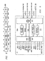
Figure 3 is a block diagram illustrating emulation device 6
in more detail. CPU core 102a will be described in more detail
with respect to Figure 4. A memory bus bridge 300 external to,
but located close to the core, supports two copies of the memory
bus, Port 0 and Port 1. To accommodate memory configurations of
various target systems, emulation device 6 contains memory
blocks 310-317 that can be mapped to any non-overlapping binary
boundary memory location within the addressable space of the
core. The replacement memory blocks are segmented into two
groups, group 1 being blocks 314-317 and group 2 being blocks
310-313. Within each group, two blocks of the same size can be
linked to form a larger memory block, according to an aspect of
the present invention. For each block, configuration registers
enable the user to program the location of the block-via the
JTAG port or via the user application software. A separate
reset line (MEMRS) exists for these configuration registers such
that during normal reset operations, the programmed memory
locations of the blocks are not corrupted. The memory blocks
can also be configured to emulate ROM and single-access RAM
(SARAM), and read operations from flash memory. The total
replacement memory size is 108K words by 16 bits (excluding
fixed memory blocks B0 and B1). Group 1 blocks are connected to
Port 1 and Group 2 blocks to Port 0.
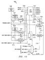
Each replacement memory block can respond to a program
space read or write request and a data space read or write
request. Separate wait state request signals are generated by
each memory block for each type of request in response to
arbitration circuitry within each memory block, which will be
described in more detail with respect to Figures 10-12. All of
the wait state signals of each type from all of the blocks of
memory are ANDed together and provided to pipeline control
circuitry within the CPU core to cause the pipeline to stall if
a memory block requests a wait state.
Emulation device 6 also contains two single access random-access
memory (SARAM) blocks, called B0 and B1, which are 1K
words in size. Block B1 can also be configured to emulate
mirroring for target devices that use smaller blocks. B0 and B1
are connected to Port 0.
External interface (XINTF) 320 is the connection to target
systems. This asynchronous interface consists of 22 address
lines and 16 data lines. It supports connection to 8-bit or 16-bit
memories/peripherals, and supports 8-bit, 16-bit, and 32-bit
data transfers. Each of the eight zones in the XINTF can be
mapped to any non-overlapping binary boundary within the
addressable space and supports emulation of
microprocessor/microcomputer mode (for ROM emulation). The XINTF
can also be programmed with different numbers of wait states for
specified memory zones. Configuration and control registers,
accessible via the JTAG port or the user application code,
configure the modes of operation. The external interrupt lines
can also be programmed for level or edge detection, and
synchronization logic can be disabled.
Function generator 330 is included in the emulation device
for use in silicon test and debug efforts. It is used to
generate various interrupt waveforms to assist in the debug of
interrupt events.
PLL block 331 enables the user to program (via external
jumpers) various fixed frequency multiples and modes. It can
source the external clock from the emulation system (XDSCLK) or
from the target system (TARGETCLK). The PLL block can also be
disabled and either of the external clocks fed directly to the
core.
Reset block 332 filters and distributes the various system
resets necessary for the emulation device. The XDSRS and
TARGETRS signals reset the core and any peripheral operating
mode configuration registers. The MEMRS signal resets any
memory or peripheral mapping registers. The mapping of any
memory or peripheral is not affected by the XDSRS and TARGETRS
signals. The reset block also synchronizes the various
asynchronous reset inputs to the device clock.
Pipeline flattener 333 aligns the instruction decode, read
and write phases of the pipe such that the information for each
instruction is "flattened" for ease of tracing by an external
logic analyzer. This block attaches to a visibility port 334
and Port 1 of the memory bus of the CPU.
Range logic 335 is used to provide some additional
triggering capability for external logic analyzer tracing.
Timer 0 336 and timer 1 337 are identical 16-bit timers
with presettable periods and with clock prescaling. The timers
have a 16-bit count-down register that generates an interrupt
and sets/toggles an output pin when the counter reaches- 0. The
counter is then automatically reloaded with the period value.
The timer configuration registers can be remapped anywhere in
the target processor core address map, this allows the emulation
device to substitute any target device timers with similar
functionality.
Test block 338 contains two multiplexers that enable
probing certain internal emulation device signals that are not
pinned out.
All peripherals and memories attached to the memory bus
ports prioritize memory accesses. Generally, the priority of
memory bus accesses can be summarized as shown in Table 1.
| Priority of Memory Bus Accesses |
| Highest: | Data Writes (see Note 1) |
| Program Writes (see Note 1) |
| Data Reads |
| Program Reads (see Note 2) |
| Lowest: | Instruction Fetches (see Note 2) |
| NOTES: 1. Simultaneous data and program writes cannot occur on the memory bus. |
| 2. Simultaneous program reads and fetches cannot occur on the memory bus. |
Figure 4 is a more detailed block diagram of DSP core 102
and 102a. The core consists of a central processing unit (CPU)
400, emulation logic 402, and memory control signals 403 and
interrupt signals 404 for interfacing with memory and
peripherals. It also includes six interface buses 410-415: three
22-bit address buses and three 32-bit data buses. The core is
implemented in a modified Harvard architecture, which uses
multiple memory spaces to enable instruction and data fetches to
be performed in parallel, allowing single-cycle instructions.
The CPU can read instructions and data while it writes data
simultaneously to maintain the single-cycle instruction
operation across the pipeline. The CPU does this over the six
separate address/data buses.
FIGURE 5 is a more detailed block diagram of processor 100,
showing core 102 and memory system 524. Memory system 524
includes both a program memory 516 and a data memory 518.
Processor 100 includes a pipeline 20. Pipeline 20 includes
a prefetch stage 24, a fetch stage 26, a decode stage 28, a read
stage 30, an execute stage 32, and a store stage 34. Processor
100 may also include additional processing elements 21.
Prefetch stage 24 obtains an instruction from a memory
location in program memory 516. Prefetch stage 24 issues a
memory address to program memory 516, and an instruction stored
in the location in program memory 516 that corresponds to that
address is provided to prefetch stage 24. An address is provided
by prefetch stage 24 to program memory 516 on instruction
address bus 36. An instruction is returned to prefetch unit 24
from program memory 516 on instruction bus 38. Prefetch stage
24 includes a program counter 58 that generates an address
corresponding to an instruction stored in program memory 516.
Prefetch stage 24 may be replaced with more than one pipeline
stage. For example, prefetch stage 24 may be replaced with a
separate stage that performs the function of computing an
address of the memory location in program memory 516 from which
to read an instruction and a separate stage that performs the
function of reading the instruction from the specified address.
However, as used hereinafter, "prefetch stage" refers to the
stage in a pipeline that actually calculates an address from
which an instruction is to be obtained.
Decode stage 28 decodes the instruction obtained from
program memory 516. Read stage 30 reads from data memory 518
any data necessary for execution of the instruction decoded by
decode stage 28. Decode stage 28 and Read stage 30 may-each be
replaced with more than one stage. For example, Decode stage 28
may have a first stage that performs a gross decode to determine
a class of instructions, for example, and a second stage that
does a fine decode of the various instruction fields, for
example. Likewise, read stage 30 may be replaced by a separate
stage that performs a computation necessary to determine from
which location in data memory 518 data will be read, and a
separate stage that performs the function of reading such data.
Execute stage 32 performs the function of executing the
instruction decoded by decode stage 28. Although execute stage
32 may be divided into a plurality of stages, as used
hereinafter, "execute stage" refers to a stage in a pipeline
that performs at least the function of determining if a
condition associated with a conditional call is met. Store
stage 34 performs the function of writing any data that may be
required to be written as a result of the execution of
instruction 38.
Store stage 34 performs the function of writing any data
that may be required to be written after execution of
instruction, such as a result.
For simplicity, only single stages for each of the
categories discussed above will be shown in the following timing
diagrams, however one skilled in the art can readily apply the
teachings herein to instruction execution pipelines that have
fewer or more stages.
Referring again to Figure 3, emulation device 6 provides a
large amount of on-chip RAM to allow for code development.
Memory consists of blocks that can be reconfigured into varying
sizes. Each block can be assigned different starting addresses
for both program address space and data space with different
attributes. For example, a block can be configured as read-only
memory or it can be configured to imitate the timing of
different types of memory. Two blocks of the same size can be
combined to form a larger block. A memory block can- support
only one memory access at a time, but is connected to all three
address buses 410, 412, 414 and can receive up to three
simultaneous memory requests. Simultaneous accesses to a block
or to a grouped block can introduce memory stalls.
This embodiment of emulation device 6 supports up to 108K
by 16 words of replacement memory, excluding blocks B0 and B1.
Memory blocks B0 and B1 are used for basic operation of the
processor core and for testing; they are therefore isolated from
the other memory blocks. The replacement memory blocks can be
mapped to program space, data space, or both. They also can be
mapped to different address boundaries in either program or data
space. The memory blocks available in the present embodiment
include: two blocks 316/317of 32K words by 16 bits; two blocks
314/315 of 16K words by 16 bits; two blocks 310/311 of 4K words
by 16 bits; and two blocks 312/313 of 2K words by 16 bits. One
skilled in the art will realize that in another embodiment the
memory block sizes may be freely changed and still embody
aspects of the present invention.
Figure 6 is a block diagram illustrating how pairs of
memory blocks can be linked to emulate larger blocks of memory,
according to an aspect of the present invention. For example,
32k-word memory block 316 can be merged with 32k-word memory
block 317, as indicated by link 610, to form a 64k-word merged
memory block. The memory blocks can be mapped only to binary
boundaries, which are equal to the total block size. For
example, a 16K block can be mapped only at every 16K boundary.
If two blocks are merged, for example, if 4K block 310 is merged
with another 4K block to form an 8K block, the combined block
size must be mapped on an 8K binary boundary. One skilled in
the art will realize that in another embodiment of the present
invention, various mapping techniques can be included in each
memory block so that different boundary conditions exists, or
even so that no boundary conditions exist.
Figure 7 illustrates a representative start--
address
register 700. Each memory block contains two start address
registers; one for program space and one for data space. Table
2 shows the bit definitions for a program start address
register, referred to as PSTRT. Since the present embodiment of
emulation device 6 has eight memory blocks, there are eight
PSTRT registers and each one uses this same format.
| Program Start Address Register Bit Definitions |
| NO. | FUNCTION |
| 15-n | PSTRT[15:n]. Maps the memory block to a location in program space. The higher bits of the program address bus, PAB[21:m] (m = 10-14) are compared with the PSTRT[15:n] (n = 4-8) bits to determine whether the memory is selected. The number of bits compared depends on the size of the memory block, as shown in Table 5. |
Table 3 lists the address bit comparison that is used for
the various sizes of memory. In the present embodiment, each
memory block is constrained to start at a defined binary block
location so that at most ten address bits are required to define
the starting address of the memory block. To calculate the value
to load in a PSTRT register, the desired starting address must
be aligned to the appropriate boundary, and that address is
divided by 64. For example, a 4K block on an 8K boundary can
arbitrarily be placed at address 2000h, as indicated in Figure 7
on
program address bus 701. Dividing by 64 or right shifting by
6 obtains a value of 0080h for the register, as illustrated in
Figure 7 where a value of 0080h is stored in
PSTRT register 700.
| PSTRT Bit Comparison |
| BLOCK SIZE | BOUNDARY | COMPARISON BETWEEN |
| 1K x □ 32 | 2K | PAB[21:11] | PSTRT[15:5] |
| 2K x 32 | 4K | PAB[21:12] | PSTRT[15:6] |
| 4K x 32 | 8K | PAB[21:13] | PSTRT[15:7] |
| 8K x 32 | 16K | PAB[21:14] | PSTRT[15:8] |
| 16K x 32 | 32K | PAB[21:15] | PSTRT[15:9] |
Table 4 shows bit definitions for a data address start
register, referred to a DSTRT. All eight DSTRT registers for the
replacement blocks use this same format. Similarly to PSTRT
registers, to calculate the value of a DSTRT register, first
determine the desired starting address, making sure it is
aligned to the appropriate boundary, and divide that address by
64, as listed in Table 5.
| DSTRTG1_1 Register-Bit Definitions |
| NO | FUNCTION |
| 15 -n | DSTRT[15:n]. Maps the memory block to a location in data space. The higher bits of the data-read address bus, DRAB[21:m], and the data-writeaddress bus, DWAB[21:m] (m = 10-14), are compared with the DSTRT[15:n] (n = 4-8) bits to determine whether the memory is selected. Table 7 shows the number of bits compared at different block sizes. |
| DSTRT Bit Comparison |
| BLOCK SIZE | BOUNDARY | COMPARISON BETWEEN |
| 512 x 32 | 1K | DAB[21:10] | DSTRT[15:4] |
| 1K x 32 | 2K | DAB[21:11] | DSTRT[15:5] |
| 2K x 32 | 4K | DAB[21:12] | DSTRT[15:6] |
| 4K x 32 | 8K | DAB[21:13] | DSTRT[15:7] |
| 8K x 32 | 16K | DAB[21:14] | DSTRT[15:8] |
Figure 8 illustrates a
memory control register 800,
referred to as a MCTL register. Each of memory block has a MCTL
register and all eight MCTL registers use this same format.
Table 6 defines each bit of
MCTL register 800.
| MCTLG1_1 Register Bit Definitions |
| NO. | NAME | FUNCTION |
| 15-12 | Rsvd | Reserved | |
| 11 | HIBANK | High bank enable bit. HIBANK, when set to 1, indicates that the current block is the high bank of the merged memory block. When set to 0, it indicates that the current block is the low bank of the merged memory block. If blocks are not merged, this bit must be set to 0. See default memory map for value after MEMRS. |
| 10 | MERGE | Merge memory block. This bit, when set to 1, indicates that the current block is merged with its corresponding partner. When set to 0, the block is not merged with its corresponding block (see Figure 5). Both merged blocks must have this bit set. See default memory map for value after MEMRS. |
| 9 | ROMMODE | ROM mode enable bit. This bit, when set to 1 enables the memory block to respond to the current state of the MPNMC input signal to the memory wrapper. If the MPNMC signal is high, the memory block is disabled from the memory map. If the MPNMC signal is low, the memory block is enabled. If the ROMMODE bit is set to 0, the current state of the MPNMC input signal is ignored. This bit applies only to Group 1 memory blocks. All other memory blocks ignore this bit. The PON and DON bit states are ignored if the block is disabled. |
| 8 | Rsvd | Reserved |
| 7-4 | WS [3:0] | Wait states. These bits indicate the number of wait states that must be introduced for any access (read or write) to this block. The number of wait states corresponds to the value of this field (i.e., 0000b = 0 wait state, 0001b = 1 wait state, 0010b = 2 wait states, etc.). WS defaults to 0 wait state on memory reset (MEMRS).0-15 wait states are supported. |
| 3 | Rsvd | Reserved | |
| 2 | READO | Read-only. If this bit is set, write accesses are ignored unless DBGACC is asserted (the TMP320C2700-E3 signal enables emulation software to download to read-only memory). READ0 defaults to zero on memory reset (MEMRS) to enable read/write mode. |
| 1 | DON | Data memory on. The block is mapped to data space when this bit is set. The value of DSTRT can be freely modified while this bit is cleared. See default memory map for value after MEMRS. See Table 9. |
| 0 | PON | Program memory on. The block is mapped to program space when this bit is set. The value of PSTRT can be freely modified while this bit is cleared. See default memory map for value after MEMRS. See Table 9. |
As discussed above, in the present embodiment of a
customizable digital signal processor (cDSP) emulation device 6,
memory blocks are aligned to the nearest binary boundaries. For
example, a 12K SARAM block can be mapped only on every 16K
boundary. Therefore, if two SARAM blocks are linked together,
the combination of the two blocks must be mapped via the
PSTRT/DSTRT registers to the nearest binary boundary- of the
combined block size. Referring again to Figure 6, if MERGE = 1
on MCTLG1_3 and MCTLG1_1, then blocks 316 and 317 are linked.
If MERGE = 1 on MCTLG1_4 and MCTLG1_5, then blocks 314 and 315
are linked. If MERGE = 1 on MCTLG2_1 and MCTLG2_1, then blocks
310 and 311 are linked. If MERGE = 1 on MCTLG2_3 and MCTLG2_4,
then blocks 312 and 313 are linked.
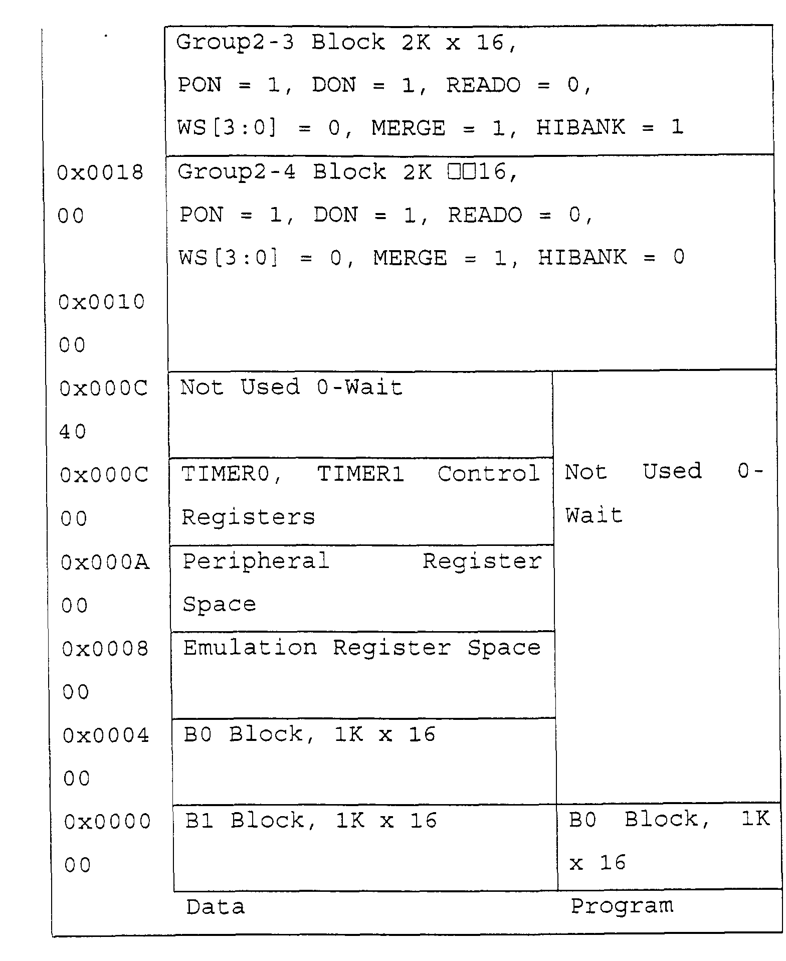
Table 7 shows the default memory map for
emulation device
6. The default memory map is set by a valid
MEMRS signal. The
XINTF is mapped at the top of program and data space such that
it is possible to boot the emulation device from external
memory.
Figure 9 is a block diagram illustrating external interface
(XINTF) 104a in more detail. XINTF 104a is similar to XINTF 104
on target device 10. Referring again to Figure 2, emulation
device 6 is connected to target device 10 by connecting between
XINTF 104 of target device 10 and XINTF 104a of emulation device
6 with a bus 11. Bus 11 is a cable in this embodiment which
connects to a connector, not shown, provided on target system 2
and another connector, not shown, on emulator interface 5.
The XINTF bus 122 is the primary strobe-based interface for
standard asynchronous memories and peripherals on target device
10. CPU core 102 does not have a dedicated bus defined for
peripheral operations. Separate blocks of logic are--used to
interface I/O blocks to the memory buses of the core. XINTF
block 104a maps the signals of the memory protocol to a smaller
bus intended primarily for interfacing to off-chip components.
The XINTF multiplexes the separate program, data-read, data-write
buses from CPU core 102 memory buses 410-415 into a 22-bit
address bus, XA[21:0], and a 16-bit data bus, XD[15:0] which
forms bus 122. External bus 122 can support 32-bit, 16-bit, and
8-bit data reads and writes to external memories or peripherals.
It also generates wait states for slow external memory accesses.
While only 16 data lines are supported on emulation device 6,
XINTF 104a performs packing/unpacking of 32-bit data. The XLONG
output signal indicates that a 32-bit operation is in progress.
XINTF 104a supports program-tracing through the visibility
mode. It also can support direct memory access (DMA) and cache-data
transfers that share the external buses.
XINTF 104a also filters the external-interrupt signals,
XINT1 to XINT14 and external non-maskable interrupt signal XNMI
and forms internal interrupt signals INT1-14 and NMI. Each of
the interrupts goes through an interrupt
filter block 910, which
can be configured in one of the three modes listed in Table 8.
Each interrupt line can be configured independently to operate
in any of the three modes.
| Interrupt modes |
| Level | : not synchronized, feed the interrupt directly to the core. The interrupt input line must meet setup and hold times relative to the XCLKOUT signal and the action has no conditioning for the interrupt to be recognized. Multiple interrupts occur if the interrupt line is held low. |
| Level: | synchronize the interrupt signal to the processor clock without edge detection. The interrupt is latched two cycles after the interrupt line goes low. There are no setup and hold time requirements. Multiple interrupts occur if the interrupt line is held low. |
| Leading-edge: | synchronize the input and detect the leading edge. The leading edge is detected if the interrupt line is held high for one clock cycle and low for one clock cycle. No additional interrupts are generated if the interrupt line is held low for longer than one cycle. The XINTF bridge issues a synchronized one-processor-cycle pulse for each assertion of the interrupt. This adds clock delay but allows for an asynchronous input. |
XINTF 104a can be remapped in memory, just like the memory
blocks. Because the XINTF does not have a fixed size, both
starting and ending addresses must be specified for it. XINTF
bridge 920 contains several configuration registers that are
read and written from the memory bus side of the bridge. The
registers are used to: set up bus timing, specify how interrupts
reconditioned, control write buffer depth, and specify other
options. The registers should be initialized by system software
during the power-up process.
XINTF 104a can be mapped into eight independent zones.
Each zone has a configuration register for specifying the start
address and the range (or block size). XINTF timing can be
configured by zone basis in either data or program space. Each
zone can also be configured to ignore the XREADY signal,
allowing switching between a fast memory device with a known
number of wait states and a slow device that uses the XREADY
signal to increase the number of wait states.
XINTF 104a includes buffer block 930 which has 5 volt
tolerant buffers for each signal on bus 11.
Figure 10 is a block diagram illustrating a memory block
1000 representative of each of the replacement memory blocks of
Figure 3 in more detail. Memory block 1000 has memory circuitry
1010 with a capacity of 4k x 16 bits, for example. Each memory
block is connected to program address and data bus 1012/1015,
data read address and data bus 1013/1016 and data write address
and data bus 1014/1017. Three wait state request signals;
program space read ready POREADY, data space read ready
DROREADY, and data space write ready DWOREADY; are generated by
arbitration circuitry 1050 and connected to the CPU instruction
pipeline control circuitry, as described earlier, for requesting
wait states. A program ready output (PRDYOUT) signal 1021 and a
data read ready output (DRDYOUT) signal 1022 are generated by
arbitration circuitry 1050 and are daisy-chained to other memory
blocks and ultimately connected to the CPU to indicate that a
program word or a data word will be available at the end of the
wait state period. A program ready input (PRDYIN) signal 1023
and a data read ready input (DRDYIN) signal 1024 are received by
arbitration circuitry 1050 as part of the daisy-chain from other
memory blocks. Wait state signals and ready signals are
described in more detail with respect to Figures 11 and 12.
A memory control register 1030 as described with reference
to Figure 9 is included in each memory block 1000. A program
start register 1031 and a data start register 1032 as described
with reference to Figure 8 is included within each memory block
1000. A block size register 1035 specifies the word capacity of
memory circuitry 1010. Block size register 1035 is implemented
as a read only fixed value when memory block 1000 is
instantiated, but may be writable in another implementation.
A separate decode circuit 1040-42 is associated with each
address bus 1012-15 and determines when an address presented on
an address bus is within a range established by start address
registers 1031 and 1032 and block size register 1035. Since up
to three memory requests can be received on each of the three
address buses 1012-15, an arbitration circuit 1050 determines
which request will be serviced. Non-serviced requests are
queued. A write request is highest priority as indicated in
Table 1. An address multiplexor 1060 is connected to
arbitration circuit 1050 and selects the highest priority
address bus and connects it to a memory circuit address bus
1018. A data multiplexor 1061 is also connected to arbitration
circuit 1050 and connects a memory circuit data bus 1019 to a
respective data bus 1015-17 associated with the highest priority
address bus. Once the highest priority request has been
selected, a corresponding wait signal is asserted if a wait
state is needed, as defined by wait state field 1030a of memory
control register 1030. Also, either PRDYOUT signal 1021 or
DRDYOUT signal 1022 is asserted in response to the selected
request.
According to an aspect of the present invention, two memory
blocks 1000 can be merged together by setting the merge bit in
memory control register 1030. A merge signal 1030b is provided
to each decoder circuit 1040-42, which causes the decoder to
mask the high bit of the address block, as specified by block
size register 1035. This bit is referred to herein as the
relative most significant bit (msb), since it is the msb of the
block of addresses, but not necessarily the msb of the complete
address. Thus, both merged memory blocks respond to memory
requests in an identical locked stepped manner to advantageously
emulate a larger memory block. Otherwise, one memory block 1000
could respond to a program request, for example, while a second
merged block 1000 responds to a data request, for example; this
would not be a correct emulation of a large block of memory. In
order for the correct memory circuit 1010 to respond to the
selected memory request, a bank decoder 1070 compares the high
bank signal 1030c from control register 1030 to the relative msb
address bit corresponding to the block size indicated by block
size register 1035 to determine if a received address is within
a preselected address bank indicated by the control register.
Thus, two memory blocks 1000 can be merged by appropriate
setting of the control register and starting address registers
and operate in lock step to simultaneously arbitrate and select
a same one of several memory requests and to respond to the
selected memory request by operating only one memory circuit
1010, as selected by a relative msb address bit.
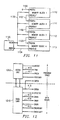
Figure 11 is a block diagram of representative memory
blocks which illustrates the program space ready daisy chain.
As discussed above, each memory block is connected to both a
program space ready (PRDY) daisy chain and to a data space ready
(DRDY) daisy chain; however only the PRDY daisy chain is
illustrated for simplicity. In Figure 11, only four memory
blocks 1110-14 are illustrated, for simplicity.
The PRDY and DRDY signals are defined as inputs to CPU core
1120 that indicate to the CPU that a memory is responding with
valid data to a read request from the CPU. Since many memories
and other components can be connected to the memory interface,
the PRDY and DRDY signals must be driven active to the CPU every
time a component is responding to a read request by having each
component generate a PRDY or DRDY output and "ORing" all these
before sending them to the CPU. For systems where multiple
blocks of memory are present, the interfaces use a daisy-chain
for the PRDY or DRDY signals. Every component has a PRDY/DRDY
input and a PRDY/DRDY output. The PRDY daisy chain illustrated
in Figure 11 is formed by daisy chain signals 1100-1104, which
are connected between the PRDYOUT signal and the PRDYIN signal
of sequential memory blocks. Initial daisy chain signal 1100 is
connected to logic 0 and final daisy chain signal 1104 is
connected to the PRDY input on CPU core 1120. The output signal
of any component goes active when either it is responding to a
memory request or its input signal is active. Emulation device
6 and target device 10 have PRDY and DRDY daisy chains
implemented in a similar manner.
Figure 12 is a block diagram of the instruction execution
pipeline of CPU core 102 and 102a, illustrating aspects of
decoupled fetch unit 1200 and the various wait signals.
Decoupled fetch unit 1200 corresponds to prefetch stage 24 in
Figure 5, while data pipeline unit 1210 includes instruction
pipeline read stage 30 and store stage 34 of Figure 5.
Decoupled fetch 1200 unit runs independently of pipeline unit
1210, allowing the fetch unit to continue issuing fetches while
the data pipeline unit has stalled. The reverse is also true.
The data pipeline can continue with its operations even if the
fetch unit is stalled. The fetch unit uses a set of program
space memory interface signals to perform instruction fetches
and data accesses to program space. The fetch unit keeps the
internal buffer full by prefetching instructions. The data
pipeline works off the internal buffers and freezes the pipeline
only when there are no instructions in the buffer. A memory can
request wait states whenever it needs extra cycles to complete a
request, as described with reference to Figure 11. Even though
the core has a two-staged pipelined read, the memory block must
request wait states for a read at the first cycle where the read
request is sent out by the CPU. The memory block cannot request
a wait state when it is driving the data out on the second phase
of the read. Therefore, timing of the wait signals is critical.
For simplicity, not all of the memory interface signals are
shown.
As described with respect to Figure 10, wait signals
POREADY, DROREADY, and DWOREADY are generated by arbitration
circuitry in each memory block to send a request for additional
wait states when the memory block cannot complete an operation
within one cycle. All memories and components connected to the
memory interface normally have the POREADY, DROREADY, and
DWOREADY output held high. Only when a component recognizes
that an access requires wait states does it pull the POREADY,
DROREADY, and DWOREADY low.
Memory reads are pipelined in two stages. The CPU has two
pipeline stages for all read operations. The core uses single-edge
clocking; therefore, all core output signals are driven out
on a clock edge and all input signals are sampled during a clock
edge. At the start of a read cycle, address and strobes are
asserted by the CPU. Memory blocks and other components decode
the address and strobes to identify if the access is meant for
that block. If the access is meant for that block and the block
needs more cycles to complete the read operation, POREADY or
DROREADY is pulled low before the next clock edge. This causes
the CPU to freeze the pipeline (on data reads) and remain in
this condition until the memory component that requested the
wait state pulls the POREADY or DROREADY signal high again. On
the cycle after POREADY or DROREADY goes high, the data is
driven to the CPU along with PRDY or DRDY. The CPU latches the
data at the next clock edge. In this embodiment, this timing
relation is important and must be followed. POREADY or DROREADY
must be asserted high exactly one cycle before the data and PRDY
or DRDY is to be driven back to the CPU. One skilled in the art
will recognize that another embodiment of the present invention
may have different timing restrictions, or may dispense-with the
PRDY or DRDY signals altogether.
Program space writes use PAB 410 as the address bus, DWDB
415 as the data bus and PWDS0 and PWDS1 as the write-select
strobes. Data space writes use DWAB 414 as the address bus, DWDB
415 as the data bus, and DWDS0 and DWDS1 as the write-select
strobes. Address, data and write-select strobes are asserted by
the CPU on a clock edge 1. If a data-space write requires wait
states, the DWOREADY signal must be pulled low by the selected
memory block before a clock edge 2. If the write completed
successfully, DWOREADY goes high and the pipeline advances.
Advantageously, by merging memory blocks and masking a msb of
the address to the arbitration circuitry, generation of the wait
signals proceeds as if each memory block was still independent
so that critical timing of the wait signals is not compromised.
Fabrication of emulation device 6 involves multiple steps
of implanting various amounts of impurities into a semiconductor
substrate and diffusing the impurities to selected depths within
the substrate to form transistor devices. Masks are formed to
control the placement of the impurities. Multiple layers of
conductive material and insulative material are deposited and
etched to interconnect the various devices. These steps are
performed in a clean room environment.
A significant portion of the cost of producing the data
processing device involves testing. While in wafer form,
individual devices are biased to an operational state and probe
tested for basic operational functionality. The wafer is then
separated into individual dice, which may be sold as bare die or
packaged. After packaging, finished parts are biased into an
operational state and tested for operational functionality.
An alternative embodiment of the novel aspects of the
present invention may include other circuitries, which are
combined with the circuitries disclosed herein in order to
reduce the total gate count of the combined functions. Since
those skilled in the art are aware of techniques for gate
minimization, the details of such an embodiment will not be
described herein.
Thus, there has been described an emulation device for
connecting to a target system in which variable size of memory
can be configured to emulate customized blocks of memory in the
target device.
Advantageously, blocks of memory in the emulation device
can be linked together to form a single block of memory that
operates in the same manner as a single block of memory.
Arbitration circuitry in each block of memory operates in lock
step by simply masking an address msb as an address is presented
to the address decoders of the arbitration circuitry. By
masking the msb address bit, each of the linked memory blocks
responds to the address in the same manner, so that the linked
memory blocks operate as a single memory block.
Advantageously, by masking an address bit in the
arbitration circuitry, timing sensitive wait state signals from
each linked memory block do not need to be interconnected.
In another embodiment, more than two memory blocks could be
interconnected to form a single merged memory block.
In another embodiment, blocks of different size could be
linked by providing suitable mapping circuitry.
As used herein, the terms "applied," "connected," and
"connection" mean electrically connected, including where
additional elements may be in the electrical connection path.
Insofar as embodiments of the invention described above are
implementable, at least in part, using a software-controlled
programmable processing device such as a Digital Signal
Processor, microprocessor, other processing devices, data
processing apparatus or computer system, it will be appreciated
that a computer program for configuring a programmable device,
apparatus or system to implement the foregoing described methods
is envisaged as an aspect of the present invention. The computer
program may be embodied as source code and undergo compilation
for implementation on a processing device, apparatus or system,
or may be embodied as object code, for example. The skilled
person would readily understand that the term computer in its
most general sense encompasses programmable devices such as
referred to above, and data processing apparatus and computer
systems.
Suitably, the computer program is stored on a carrier
medium in machine or device readable form, for example in solid-state
memory or magnetic memory such as disc or tape and the
processing device utilises the program or a part thereof to
configure it for operation. The computer program may be
supplied from a remote source embodied in a communications
medium such as an electronic signal, radio frequency carrier
wave or optical carrier wave. Such carrier media are also
envisaged as aspects of the present invention.
While the invention has been described with reference to
illustrative embodiments, this description is not intended to be
construed in a limiting sense. Various other embodiments of the
invention will be apparent to persons skilled in the art upon
reference to this description. It is therefore contemplated
that the appended claims will cover any such modifications of
the embodiments as fall within the true scope and spirit of the
invention.
The scope of the present disclosure includes any novel
feature or combination of features disclosed therein either
explicitly or implicitly or any generalisation thereof
irrespective of whether or not it relates to the claimed
invention or mitigates any or all of the problems addressed by
the present invention. The applicant hereby gives notice that
new claims may be formulated to such features during the
prosecution of this application or of any such further
application derived therefrom. In particular, with reference to
the appended claims, features from dependent claims may be
combined with those of the independent claims and features from
respective independent claims may be combined in any appropriate
manner and not merely in the specific combinations enumerated in
the claims.