EP1111817A2 - Optical communication receiver - Google Patents
Optical communication receiver Download PDFInfo
- Publication number
- EP1111817A2 EP1111817A2 EP00127977A EP00127977A EP1111817A2 EP 1111817 A2 EP1111817 A2 EP 1111817A2 EP 00127977 A EP00127977 A EP 00127977A EP 00127977 A EP00127977 A EP 00127977A EP 1111817 A2 EP1111817 A2 EP 1111817A2
- Authority
- EP
- European Patent Office
- Prior art keywords
- signal
- code decision
- decision
- units
- code
- Prior art date
- Legal status (The legal status is an assumption and is not a legal conclusion. Google has not performed a legal analysis and makes no representation as to the accuracy of the status listed.)
- Withdrawn
Links
Images



Classifications
-
- H—ELECTRICITY
- H04—ELECTRIC COMMUNICATION TECHNIQUE
- H04B—TRANSMISSION
- H04B10/00—Transmission systems employing electromagnetic waves other than radio-waves, e.g. infrared, visible or ultraviolet light, or employing corpuscular radiation, e.g. quantum communication
- H04B10/60—Receivers
- H04B10/66—Non-coherent receivers, e.g. using direct detection
- H04B10/69—Electrical arrangements in the receiver
- H04B10/697—Arrangements for reducing noise and distortion
Definitions
- the present invention relates to an optical transmission system using RZ (Return to Zero)-modulated signals and, more particularly, to an optical communication receiver with excellent resilience against the distortion of signal light in the timing direction (phase direction).
- RZ Return to Zero
- soliton optical transmission scheme As a technique of realizing high-bit-rate transmission, a soliton optical transmission scheme has received a great deal of attention.
- a characteristic feature of soliton optical transmission is that a nonlinear effect in a transmission path optical fiber, which is generally a factor responsible for a deterioration in signal wavelength, is positively used for stable transmission of a signal waveform. For this reason, the soliton optical transmission scheme allows long-distance, high-speed optical communication which cannot be attained by other schemes.
- wavelength multiplexing transmission when soliton optical transmission is tried in each channel, transmission is not so stable as in a single channel, and the signal waveform after transmission is distorted. This is because interaction between the channels is produced by a nonlinear optical effect in the transmission path optical fiber.
- Figs. 1A to 1C respectively show the eye patterns of waveforms in a system using the above RZ-modulated signals.
- Fig. 1A shows an eye pattern without any waveform distortion.
- Fig. 1B shows an eye pattern with a waveform distortion in the amplitude direction.
- Fig. 1C shows an eye pattern with a waveform distortion in the timing direction.
- waveform distortions are accounted by those in the two directions that are superposed on each other.
- a characteristic feature of wavelength multiplexed soliton optical transmission is that the waveform distortion in the timing direction becomes more noticeable to degrade transmission characteristics (see Linn F. Mollenauer et. al., Journal of Lightwave Technology, vol. 9, pp. 362, 1991).
- Fig. 2 shows the arrangement of a communication optical receiver that is generally used. An illustration of an electric amplifier is omitted because it is not relevant to the following description.
- Fig. 3 shows how this receiver receives a signal with distortion in the timing direction. Referring to Fig. 3, decision timings and decision amplitudes are indicated by the dotted lines, and the intersections ("T" in Fig. 3) of the dotted lines represent decision points. Although the decision timing is set in the center of each bit, decision errors have occurred at the second and fourth bits from the left owing to signal waveform fluctuations in the timing direction.
- Various attempts have been made to develop a method of setting an optimal decision timing For example, a plurality of decision units are prepared to identify a signal at different timings, and a signal identified at an optimal timing is selected by using a proper method.
- Japanese Unexamined Patent Publication No. 62-159545 or 11-215110 discloses a technique of selecting an optimal clock from clocks with different phases, and input data is identified with the selected optimal clock, thereby obtaining an decision output free from a band deterioration of the reception signal, jitter, and the like.
- Japanese Unexamined Patent Publication No. 8-321827 discloses a technique of preparing first and second decision/determination section for deciding input data in units of clocks, making data input to the first and second decision/determination sections and have different phases to determine the respective decision results, and selecting and outputting one of the decision data obtained by the first and second decision/determination section.
- the above conventional technique is mainly used for a burst receiver for receiving discontinuous signal packets and is especially effective when fluctuations or changes in the timing direction are sufficiently slow as compared with the bit rate.
- this technique is not effective for timing fluctuations that occur in units of bits.
- the present invention has been made in consideration of the above situation in the prior art, and has as its object to provide an optical communication receiver which can receive signal light having fluctuations in the timing direction with less digital errors.
- an optical communication receiver comprising a photoelectric converter for converting an optical signal into an electrical signal, a signal divider for dividing the electrical signal from the photoelectric converter into a plurality of signals, code decision units connected to the respective outputs of the signal divider, phase adjusters inserted in lines for feeding clocks to the respective code decision units or between the signal divider and the respective code identifiers so as to provide fixed or variable delays, and an OR circuit for ORing the outputs from the respective code decision units.
- an optical communication receiver comprising an optical demultiplexer for demultiplexing an optical input signal into a plurality of signals, photoelectric converters connected to the respective outputs of the optical demultiplexer, code decision units connected to the outputs of the respective photoelectric converters, phase adjusters which are inserted in lines for feeding clocks to the respective code decision units or between the respective photoelectric converters and the code decision units so as to give fixed or variable delays, and an OR circuit for ORing outputs from the respective code decision units.
- a plurality of code decision units with different signal decision timings are installed to let the receiver have a plurality of decision points in the timing direction. Even if, therefore, a signal has fluctuations in the timing direction, the possibility that one of the plurality of decision points becomes an optimal decision timing for the bit is high.
- the outputs from the respective decision units are ORed to obtain a receiver output.
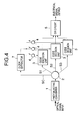
- Fig. 4 is a block diagram of an optical receiver according to the first embodiment of the present invention.
- An input signal photoelectrically converted by a photoelectric converter 1 is divided into a plurality of components (a total of four components, i.e., three components S1, S2, and S3 for a signal, and one component SC for clock reconstruction) by a signal divider 2.
- Code decision units 3 for code discrimination are connected to the respective outputs of the signal divider 2.
- a clock signal extracted by a clock extractor 7 is supplied to each code decision unit 3.
- phase adjusters 4 are adjusted to set different timings for code decision in the respective code decision units.
- Signals output from the respective code decision units 3 are ORed by an OR circuit 5, and the resultant data becomes an output from the receiver.
- a signal is branched into three components, and different decision timings (T 1 , T 2 , T 3 ) are provided for the respective components.
- T 1 , T 2 , T 3 different decision timings
- no decision unit outputs the correct input signal (110111 from the left) due to a deterioration in waveform.
- OR circuit output By calculating the OR of the outputs from the respective decision units (OR circuit output), however, decision errors due to fluctuations in the timing direction are corrected.
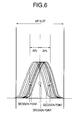
- the manner in which a difference is set between the code decision timings in the respective decision units depends on the magnitudes of fluctuations of signal light in the timing and amplitude directions. For this reason, an optimal timing difference cannot be set in a uniform manner. Assume that the fluctuations of signal light in the timing direction (phase direction) are not very large with respect to a bit slot. In this case, if the standard deviation of fluctuation amounts is represented by ⁇ , the three decision timings may be respectively set at the center of the bit slot and positions spaced apart from the center by ⁇ ⁇ .
- the respective decision timings are preferably set within ⁇ 25% of the bit slot width from the center at maximum.
- Fig. 6 shows a case wherein timing differences each corresponding to 20% of the bit slot are set between the three decision points.
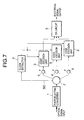
- Fig. 7 is a block diagram of an optical receiver according to the second embodiment of the present invention.
- the first embodiment of the present invention has the phase adjusters 4 on the clock feed lines.
- the second embodiment has a phase adjuster between a signal divider 2 and a code decision unit 3. With this arrangement as well, effects similar to those in the first embodiment can be obtained.
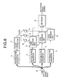
- Fig. 8 is a block diagram of an optical receiver according to the third embodiment of the present invention.
- This embodiment differs from the first embodiment in that a signal is branched while it is still signal light. With this arrangement as well, effects similar to those in the first embodiment can be obtained.
- the receiver becomes inexpensive as photoelectric converters and electric amplifiers increase in number, there is no need to perform processing that degrades signal quality, e.g., amplification and branching after photoelectric conversion.
- signal light is divided into a plurality of (three in Fig. 8) components by an optical divider 6.
- the respective components are photoelectrically converted by photoelectric converters 1 and subjected to code decision in code decision units 3.
- phase adjusters 4 placed on the clock feed lines perform timing adjustment to set differences between the decision timings in the respective code decision units.
- the signals output from the respective code decision units 3 are ORed by an OR circuit 5.
- the resultant data is output as an output signal from the OR circuit 5.
- a method of setting timing differences at the respective decision points is the same as that in the first embodiment. Referring to Fig. 8, the phase adjusters 4 are placed on the clock feed lines. Similar effects can be obtained even if the phase adjusters 4 are placed between the optical divider 6 and the photoelectric converters 1 or between the photoelectric converters 1 and the code decision units 3.
Landscapes
- Physics & Mathematics (AREA)
- Electromagnetism (AREA)
- Engineering & Computer Science (AREA)
- Computer Networks & Wireless Communication (AREA)
- Signal Processing (AREA)
- Optical Communication System (AREA)
- Synchronisation In Digital Transmission Systems (AREA)
- Dc Digital Transmission (AREA)
Abstract
Description
Claims (8)
- An optical communication receiver comprising:a photoelectric converter for converting an input optical signal into an electrical signal;a signal divider for dividing the electrical signal from said photoelectric converter into a plurality of signals;a clock extractor for reconstructing a clock of the photoelectrically converted input signal;a plurality of code decision units for performing code decision of the plurality of electrical signals divided by said signal divider at different timings; andan OR circuit for ORing outputs from said plurality of code decision units.
- A receiver according to claim 1, wherein the code decision timings of the electrical signals in said plurality of code decision units are set by fixed or variable phase adjusters which are inserted in lines for supplying signal decision timing clocks to the respective code decision units to provide the signal decision timing clocks with different delays.
- A receiver according to claim 1, wherein the code decision timings of the electrical signals in said plurality of code decision units are set by fixed or variable phase adjusters which are inserted between outputs of said signal divider and the respective code decision units to provide the respective electrical signals with different delays.
- An optical communication receiver comprising:an optical divider for dividing an input optical signal into a plurality of signals;a plurality of photoelectric converters for converting the plurality of optical signals divided by said optical divider into electrical signals;a clock extractor for reconstructing a clock of the photoelectrically converted input signal;a plurality of code decision units for performing code decision of the electrical signals output from said plurality of photoelectric converters at different timings; andan OR circuit for ORing outputs from said plurality of code decision units.
- A receiver according to claim 4, wherein the code decision timings of the electrical signals in said plurality of code decision units are set by fixed or variable phase adjusters which are inserted in lines for supplying signal decision timing clocks to the respective code decision units to provide the signal decision timing clocks with different delays.
- A receiver according to claim 4, wherein the code decision timings of the electrical signals in said plurality of code decision units are set by fixed or variable phase adjusters which are inserted between the respective photoelectric converters and the respective code decision units to provide the electrical signals output from said respective photoelectric converters with different delays.
- A receiver according to claim 4, wherein the code decision timings of the electrical signals in said plurality of code decision units are set by fixed or variable phase adjusters which are inserted between outputs of said optical divider and the respective photoelectric converters to provide the respective electrical signals with different delays.
- A receiver according to any one of claims 1 to 7, wherein the code decision timings in the respective code decision units are set with time differences within not less ±25% of a bit slot from a center of the bit slot.
Applications Claiming Priority (2)
| Application Number | Priority Date | Filing Date | Title |
|---|---|---|---|
| JP36340999A JP3498839B2 (en) | 1999-12-21 | 1999-12-21 | Optical communication receiver |
| JP36340999 | 1999-12-21 |
Publications (2)
| Publication Number | Publication Date |
|---|---|
| EP1111817A2 true EP1111817A2 (en) | 2001-06-27 |
| EP1111817A3 EP1111817A3 (en) | 2004-01-07 |
Family
ID=18479239
Family Applications (1)
| Application Number | Title | Priority Date | Filing Date |
|---|---|---|---|
| EP00127977A Withdrawn EP1111817A3 (en) | 1999-12-21 | 2000-12-20 | Optical communication receiver |
Country Status (4)
| Country | Link |
|---|---|
| US (1) | US20010015845A1 (en) |
| EP (1) | EP1111817A3 (en) |
| JP (1) | JP3498839B2 (en) |
| CA (1) | CA2328740A1 (en) |
Families Citing this family (8)
| Publication number | Priority date | Publication date | Assignee | Title |
|---|---|---|---|---|
| JP3790190B2 (en) * | 2001-12-05 | 2006-06-28 | 日本電信電話株式会社 | Digital transmission system |
| US6947214B2 (en) | 2002-04-04 | 2005-09-20 | Canon Kabushiki Kaisha | Diffractive optical element and optical system having the same |
| US7085333B2 (en) * | 2002-04-15 | 2006-08-01 | General Dynamics Decision Systems, Inc. | Constant-phase, gain-controlled amplification circuit |
| US7903982B2 (en) | 2004-04-15 | 2011-03-08 | Mitsubishi Electric Corporation | Optical receiver |
| JP5136374B2 (en) * | 2008-11-21 | 2013-02-06 | オムロン株式会社 | Optical transmission system and electronic apparatus equipped with the same |
| KR101347004B1 (en) * | 2010-09-17 | 2014-01-15 | 한국전자통신연구원 | Coherent optical receiving apparatus and method for processing thereof |
| JP5246282B2 (en) * | 2011-02-23 | 2013-07-24 | 株式会社ニコン | Imaging device and phase adjustment device |
| JP5260710B2 (en) * | 2011-08-29 | 2013-08-14 | 三菱電機株式会社 | Optical receiver |
Family Cites Families (7)
| Publication number | Priority date | Publication date | Assignee | Title |
|---|---|---|---|---|
| JPS58145258A (en) * | 1982-02-24 | 1983-08-30 | Hitachi Ltd | Received data identification circuit |
| GB2259419A (en) * | 1991-09-06 | 1993-03-10 | Northern Telecom Ltd | Direct detection of optical PSK signals |
| GB9127057D0 (en) * | 1991-12-20 | 1992-02-19 | Secr Defence | Improved digital sampling of individual pulses |
| US5473636A (en) * | 1993-02-26 | 1995-12-05 | Fujitsu Limited | Data discriminating circuit and an optical receiver using the same |
| US5557443A (en) * | 1993-12-09 | 1996-09-17 | Matsushita Electric Industrial Co., Ltd. | Optical communication method and optical remote controller |
| JPH08321827A (en) * | 1995-03-20 | 1996-12-03 | Fujitsu Ltd | Data identification device and optical receiver using the same |
| US6122335A (en) * | 1999-10-01 | 2000-09-19 | Quantum Bridge Communications, Inc. | Method and apparatus for fast burst mode data recovery |
-
1999
- 1999-12-21 JP JP36340999A patent/JP3498839B2/en not_active Expired - Fee Related
-
2000
- 2000-12-19 CA CA002328740A patent/CA2328740A1/en not_active Abandoned
- 2000-12-20 EP EP00127977A patent/EP1111817A3/en not_active Withdrawn
- 2000-12-20 US US09/739,828 patent/US20010015845A1/en not_active Abandoned
Also Published As
| Publication number | Publication date |
|---|---|
| EP1111817A3 (en) | 2004-01-07 |
| CA2328740A1 (en) | 2001-06-21 |
| US20010015845A1 (en) | 2001-08-23 |
| JP3498839B2 (en) | 2004-02-23 |
| JP2001177582A (en) | 2001-06-29 |
Similar Documents
| Publication | Publication Date | Title |
|---|---|---|
| EP2106044B1 (en) | Optical transmission system with pre-compensation and post-compensation of waveform distortion | |
| US7356256B1 (en) | Digital performance monitoring for an optical communications system | |
| EP1379042B1 (en) | Multiplexer | |
| US7920791B2 (en) | Passive optical network system and method of data transmission in the passive optical network | |
| US20030011847A1 (en) | Method and apparatus for adaptive distortion compensation in optical fiber communication networks | |
| US20040062556A1 (en) | Reception apparatus | |
| EP1111817A2 (en) | Optical communication receiver | |
| US6392770B1 (en) | Multi-point optical transmission system | |
| US6619867B1 (en) | Optical transmission system | |
| US7149432B1 (en) | Method and apparatus for equalization across plural data channels | |
| JP3311517B2 (en) | Phase comparison type bit synchronization establishment circuit | |
| JP6988604B2 (en) | Optical modulation / demodulation method, optical communication system, optical transmitter and receiver | |
| US8538265B2 (en) | Optical communication device and dispersion compensation method | |
| US6583909B1 (en) | Optical communication system and optical signal control method therefor | |
| JPH0746187A (en) | Optical communication system | |
| US20070134001A1 (en) | Polarization division multiplexed optical transmission system | |
| JP2003333014A (en) | Optical signal transmission control method and system | |
| US7379671B2 (en) | Optical transmitter | |
| JP2001119344A (en) | Optical transmission system | |
| CA1238432A (en) | Digital radio communication system | |
| GB2348786A (en) | Compensating for sampling offset using known reference signals | |
| JP2959257B2 (en) | Optical fiber communication method | |
| US20030185578A1 (en) | Receiving device for disturbed optical signals with generation of a feedback signal by correlation, and method of generating such a feedback signal | |
| US20040081235A1 (en) | Electrical signal equaliser with a transversal filter, an optical receiver, and a method for equalising an electrical signal | |
| JP3543757B2 (en) | Automatic identification phase adjustment method and method, and optical receiver having the same |
Legal Events
| Date | Code | Title | Description |
|---|---|---|---|
| PUAI | Public reference made under article 153(3) epc to a published international application that has entered the european phase |
Free format text: ORIGINAL CODE: 0009012 |
|
| AK | Designated contracting states |
Kind code of ref document: A2 Designated state(s): AT BE CH CY DE DK ES FI FR GB GR IE IT LI LU MC NL PT SE TR |
|
| AX | Request for extension of the european patent |
Free format text: AL;LT;LV;MK;RO;SI |
|
| PUAL | Search report despatched |
Free format text: ORIGINAL CODE: 0009013 |
|
| AK | Designated contracting states |
Kind code of ref document: A3 Designated state(s): AT BE CH CY DE DK ES FI FR GB GR IE IT LI LU MC NL PT SE TR |
|
| AX | Request for extension of the european patent |
Extension state: AL LT LV MK RO SI |
|
| 17P | Request for examination filed |
Effective date: 20031126 |
|
| AKX | Designation fees paid |
Designated state(s): DE FR IT |
|
| 17Q | First examination report despatched |
Effective date: 20070911 |
|
| STAA | Information on the status of an ep patent application or granted ep patent |
Free format text: STATUS: THE APPLICATION IS DEEMED TO BE WITHDRAWN |
|
| 18D | Application deemed to be withdrawn |
Effective date: 20080326 |