EP1111615A1 - Logic circuit - Google Patents
Logic circuit Download PDFInfo
- Publication number
- EP1111615A1 EP1111615A1 EP00400539A EP00400539A EP1111615A1 EP 1111615 A1 EP1111615 A1 EP 1111615A1 EP 00400539 A EP00400539 A EP 00400539A EP 00400539 A EP00400539 A EP 00400539A EP 1111615 A1 EP1111615 A1 EP 1111615A1
- Authority
- EP
- European Patent Office
- Prior art keywords
- logic
- switching means
- node
- potential
- logic output
- Prior art date
- Legal status (The legal status is an assumption and is not a legal conclusion. Google has not performed a legal analysis and makes no representation as to the accuracy of the status listed.)
- Withdrawn
Links
Images


Classifications
-
- H—ELECTRICITY
- H03—ELECTRONIC CIRCUITRY
- H03K—PULSE TECHNIQUE
- H03K3/00—Circuits for generating electric pulses; Monostable, bistable or multistable circuits
- H03K3/02—Generators characterised by the type of circuit or by the means used for producing pulses
- H03K3/353—Generators characterised by the type of circuit or by the means used for producing pulses by the use, as active elements, of field-effect transistors with internal or external positive feedback
- H03K3/356—Bistable circuits
- H03K3/356104—Bistable circuits using complementary field-effect transistors
- H03K3/356113—Bistable circuits using complementary field-effect transistors using additional transistors in the input circuit
- H03K3/35613—Bistable circuits using complementary field-effect transistors using additional transistors in the input circuit the input circuit having a differential configuration
- H03K3/356139—Bistable circuits using complementary field-effect transistors using additional transistors in the input circuit the input circuit having a differential configuration with synchronous operation
-
- G—PHYSICS
- G11—INFORMATION STORAGE
- G11C—STATIC STORES
- G11C7/00—Arrangements for writing information into, or reading information out from, a digital store
- G11C7/10—Input/output [I/O] data interface arrangements, e.g. I/O data control circuits, I/O data buffers
- G11C7/1006—Data managing, e.g. manipulating data before writing or reading out, data bus switches or control circuits therefor
-
- H—ELECTRICITY
- H03—ELECTRONIC CIRCUITRY
- H03K—PULSE TECHNIQUE
- H03K3/00—Circuits for generating electric pulses; Monostable, bistable or multistable circuits
- H03K3/02—Generators characterised by the type of circuit or by the means used for producing pulses
- H03K3/027—Generators characterised by the type of circuit or by the means used for producing pulses by the use of logic circuits, with internal or external positive feedback
- H03K3/037—Bistable circuits
-
- H—ELECTRICITY
- H03—ELECTRONIC CIRCUITRY
- H03K—PULSE TECHNIQUE
- H03K3/00—Circuits for generating electric pulses; Monostable, bistable or multistable circuits
- H03K3/02—Generators characterised by the type of circuit or by the means used for producing pulses
- H03K3/353—Generators characterised by the type of circuit or by the means used for producing pulses by the use, as active elements, of field-effect transistors with internal or external positive feedback
- H03K3/356—Bistable circuits
- H03K3/356104—Bistable circuits using complementary field-effect transistors
- H03K3/356113—Bistable circuits using complementary field-effect transistors using additional transistors in the input circuit
- H03K3/356147—Bistable circuits using complementary field-effect transistors using additional transistors in the input circuit using pass gates
- H03K3/356156—Bistable circuits using complementary field-effect transistors using additional transistors in the input circuit using pass gates with synchronous operation
Definitions
- the present invention relates to a logic circuit in a CMOS semiconductor integrated circuit etc., more particularly relates to a logic circuit serving as a flip-flop with an embedded logic function combining the functions of a 1-bit storage element operating in synchronization with a synchronization signal, that is, a flip-flop, and several logic gates located at its data input packaged into one unit.
- An integrated circuit generally performs a logical operation by a combination of logic gates and stores the results thereof in a flip-flop for use for the operation of the next cycle.
- structures very common in integrated circuits such as sequential circuits and pipelines are also configured by flip-flops and one or more logic gates arranged at the data input thereof.
- Figure 1 is a view of a first conventional example realizing a general structure of a flip-flop and logic gates arranged at the data input thereof by a static CMOS logic circuit 10.
- the desired logical function is realized by a combinational logic circuit LC11.
- a logical function output F11 thereof is supplied to a data input D of a flip-flop FF 11.
- a value of the input D is fetched in synchronization with a synchronization signal CLK and output from a data output Q.
- Figure 2 is a circuit diagram of a transistor level of the flip-flop FF11.
- the flip-flop FF11 shown in Fig. 2 is based on a master-slave type flip-flop using a CMOS transmission gate disclosed in John P. Uyemura, CMOS LOGIC Circuit Design , Kluwer Academic Publishers, pp. 278-281, 1999 and is being generally used at the present.
- the flip-flop FF11 of Fig. 2 has inverters INV11 to INV18 and CMOS transmission gates TMG11 and TMG12.
- Fig. 3 is a circuit diagram of an example of the configuration of the combinational logic circuit LC11.
- This logic circuit LC11 has a 2-input exclusive OR gate (EXOR) ER11, a 2-input exclusive negative OR gate (EXNOR) ENR11, and a 2-input HAND gate NA11.
- EXOR 2-input exclusive OR gate
- EXNOR 2-input exclusive negative OR gate
- NA11 2-input HAND gate
- PDN pulse down network
- AMD Co. the AMD Co.
- PDN-F/F PDN-F mounted type flip-flop of the AMD Co.
- Steven Hesley et al. "A 7th-Generation x86 Microprocessor", ISSCC Digest of Technical Papers , pp. 92-93, February 1999, or Alisa Scherer et al., "An Out-of-Order Three-Way Superscalar Multimedia Floating-Point", ISSCC Digest of Technical Papers , pp. 282-283, February 1999.
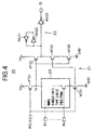
- Figure 4 is a circuit diagram of the general configuration of a PDN-F/F
- Fig. 5 is a circuit diagram of a concrete example of the configuration of a PDN-F/F logic circuit mounting a logical function of one multiplexer.
- the PDN-F/F logic circuit 20 is configured by a dynamic circuit unit 21 comprising p-channel MOS (PMOS) transistors PT21 and PT22 and n-channel MOS (NMOS) transistors NT11 to NN13 and by a static circuit unit 22 comprising inverters INV21 and INV22 with inputs and outputs connected with each other and configuring a latch and an output use inverter INV23.
- a dynamic circuit unit 21 comprising p-channel MOS (PMOS) transistors PT21 and PT22 and n-channel MOS (NMOS) transistors NT11 to NN13
- a static circuit unit 22 comprising inverters INV21 and INV22 with inputs and outputs connected with each other and configuring a latch and an output use inverter INV23.
- PDN is an abbreviation of a "pull down network” as mentioned above and is what is generally referred to as an NMOS single-rail type logic tree 23.
- the dynamic circuit unit 21 evaluates the logic, and the value thereof is held by the latch of the static circuit unit 22.
- the characterizing feature of the PDN-F/F logic circuit 20 resides in that a pulsed clock PCLK to be input to the PMOS transistor PT21 and an NMOS transistor NT21 must be a short width pulse which is generated in synchronization with the rising of the global synchronization signal CLK.
- the pulsed clock PCLK is generated by a pulse generator 24 as shown in Fig. 5.
- This pulse generator 24 is configured by an inverter INV24 to which a clock inverted signal CLK_X is input, a PMOS transistor PT23 and NMOS transistors NT24 and NT25 connected in series between a supply line of a power source voltage V DD and a ground and having gates to which the output of the inverter INV24 is supplied, a 2-input NAND gate NA21 to which a potential of a connection point of drains of the PMOS transistor PT23 and the NMOS transistor NT24 and an enable signal ENB are input, and a 2-input NOR gate NR21 to which the output of the NAND gate NA21 and the clock inverted signal CLK_X are input.
- the pulsed clock PCLK becomes the logic "1"
- the logic is evaluated in the logic tree (PDN) 23, and the node F changes.
- This change is transferred to the latch 22a comprising the inverters INV21 and INV22 through a dynamic inverter configured by the PMOS transistor PT22 and NMOS transistors NT23 and NT24. During this period, the input signal must not change.
- the important thing in the PDN-F/F logic circuit 20 is that the time during which the pulsed clock PCLK becomes the logic "0" is precisely controlled.
- This time must be the minimum time long enough for a change of the potential of the node F from the logic "1" to the logic "0".
- the time during which the pulsed clock PCLK becomes the logic "1" is directly related to the set-up time and the hold time in the PDN-F/F logic circuit 20, so a shorter width of the pulsed clock PCLK is preferred.
- the characterizing feature of the pulse generator 24 shown in Fig. 5 generating the pulsed clock PCLK resides in that an adequate width of the pulsed clock PCLK is obtained by the NMOS transistors NT24 and NT25.
- the PDN that is, the logic tree 23
- the PDN becomes three NMOS's in size. that is, if another NMOS transistor is added in series in addition to the NMOS transistors NT24 and NT25, it becomes possible to generate three NMOS's worth of delay in the pulse generator 24.
- the main object of the PDN-F/F logic circuit 20 resides in the realization of a high speed logic circuit.
- a circuit realized by a dynamic logic circuit is higher in speed than one realized by a static logic circuit.
- the master latch and the logic tree are combined with the aim of shortening the set-up time and the hold time relating to the input terminal of the logical functions.
- SA-F/F sense amplifier-based flip-flop
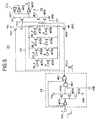
- Figure 6 is a circuit diagram of the general configuration of an SA-F/F logic circuit
- Fig. 7 is a circuit diagram of a concrete example of the configuration of a SA-F/F logic circuit mounting the logical function of one multiplexer.
- An SA-F/F logic circuit 30 is configured by an NMOS dual-rail type logic tree 31 including NMOS transistors NT301 to NT316, an NMOS transistor NT31 for controlling the connection of the NMOS dual-rail type logic tree 31 to the ground in synchronization with the clock signal CLK, a sense amplifier 32 configured by PMOS transistors PT31 to PT34, and NMOS transistors NT32 to NT34, and a NAND type SR latch 33 configured by NAND gates NA31 and NA32.
- the gate terminal of the NMOS transistor NT34 in the sense amplifier 32 is connected to the supply line of the power source voltage V DD and is always in the ON state.
- the logic inputs F and F_X by the logic tree 31 are precharged to a voltage lower than the potential of the logic "1" by the amount of the threshold value of the NMOS transistor through the NMOS transistors NT32 and NT33.
- a path through which one of the logic input node TF and TF_X with respect to the sense amplifier 32 reaches the ground is formed in the logic tree 31.
- this is the logic input node TF side.
- the NMOS transistor NT34 of the sense amplifier 32 is always ON and behaves like a real resistor, therefore the charge at the logic input node TF_X flows to the logic input node TF side through the NMOS transistor NT34.
- the potential of the logic input F_X also drops to "0" with a slight delay after the logic input F.
- the logic output node TH_X recovers to the logic "1" after the potential falls a little. This is because since the logic input F drops to the logic "0" slightly earlier, the PMOS transistor PT34 becomes ON and a charge is supplied to the logic output node TH_X. Due to this, the PMOS transistor PT33 and NMOS transistor NT33 cut off, the PMOS transistor PT34 and NMOS transistor NT32 become ON, and a stable paired logic potential state is maintained at the logic output nodes TH and TH_X.
- NMOS transistor NT33 has already become cut off and the charge of the node TH_X will not flow to the logic input node TF_X side.
- the path of the ground reaching the logic input node TF_X still only fixes the potential of the node TH at the logic "0" through the NMOS transistors NT34 and NT32.
- the main object of the SA-F/F logic circuit 30 also resides in the realization of a high speed logic circuit in the same way as the PDN-F/F logic circuit 20.
- the SA-F/F logic circuit 30 evaluates a logical function by the dynamic logic circuit in the same way as the PDN-F/F logic circuit and combines a sense amplifier and master latch with the aim of shortening the set-up time and the hold time relating to the input terminal of the logical functions.
- the differential current switch logic (hereinafter simply referred to as a "DCSL”) circuit may be mentioned (see Dinesh Somasekhar et al., "Differential Current Switch Logic: A Low Power DCVS Logic Family", IEEE JSSC, vol. 31, no. 7, pp. 981-991, July 1996).
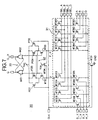
- Figure 8 is a circuit diagram of the general configuration of a DCSL circuit.
- a DCSL circuit 40 is configured by, in the same way as the SA-F/F logic circuit 30, an NMOS dual-rail type logic tree portion 41, a sense amplifier unit 42 configured by PMOS transistors PT41 to PT43 and NMOS transistors NT41 to NT45, and a NOR type SR latch 43 configured by NOR gates NR41 and NR42.
- DCSL1, DCSL2. and DCSL3 three types of sense amplifiers (DCSL1, DCSL2. and DCSL3) are proposed (pp. 983, Figs. 4 to 6).
- the DCSL3 will be taken up.
- the DCSL itself is a proposal relating to method of configuration of a new dynamic logic circuit, particularly the sense amplifier system, and is not aimed at the realization of a flip-flop with an embedded logical function.
- pp. 986, Fig. 12 introduces "a Latched DCSL output state" and suggests the realization of a flip-flop with an embedded logical function.
- the potentials of the logic outputs H and H_X of the sense amplifier 41 are set in the vicinity of the threshold voltage of the NMOS transistor.
- the potentials are treated as the logic "0" for the later logic gates referring to them.
- the clock inverted signal CLK_X is supplied with the logic "1"
- the PMOS transistor PT41 cuts off
- the NMOS transistor NT45 becomes ON.
- the internal nodes TH and TH_X are short-circuited. This means that all of the gate terminals and drain terminals of the NMOS transistors NT41, NT42, NT43, and NT44 are short-circuited.
- a MOS transistor in which the gate terminal and the drain terminal are short-circuited behaves equivalently to a diode.
- the NMOS transistors NT41, NT42, NT43, and NT44 at this time behave as diodes, therefore the current flows until the potential difference between the two ends of the diode becomes substantially equal to the threshold value of the NMOS transistor.
- the NMOS transistors NT41 and NT42 pass current to the ground, while the NMOS transistors NT43 and NT44 pass current to the logic output nodes TF and TF_X of the logic tree 41.
- the potentials of the nodes TH and TH_X become substantially equal to the threshold value of the NMOS transistor.
- the potentials of the nodes TH and TH_X are in the vicinity of the threshold voltage of the NMOS transistor. They are treated as the logic "0", so the NOR type SR latch 443 holds the output thereof.
- the clock inverted signal CLK_X becomes the logic "0" (this is equivalent to the rising of the clock signal CLK), and the logic evaluation is commenced.
- the NMOS transistor NT45 cuts off, the short-circuited state heretofore disappears, the PMOS transistor PT41 becomes ON, and the current starts to flow.
- the PMOS transistors PT42 and PT43 start from the ON state.
- the NMOS transistors NT43 and NT44 start from the cut-off state since a voltage in the vicinity of the threshold value of the NMOS transistor has been added to the gate terminals (that is, the nodes TH and TH_X).
- the charge is supplied to the nodes TH and TH_X, these node potentials rise, and the NMOS transistors NT43 and NT44 weakly start to become ON.
- the node TH_X quickly reaches the potential of the complete logic "1". Furthermore, simultaneously, the PMOS transistor PT42 becomes completely cut off, and the NMOS transistors NT41 and NT43 become completely ON.
- the stable paired logic potential state is maintained at the nodes TH and TH_X.
- the logic outputs H and H_X corresponding to the potentials of these two nodes are also the inputs of the SR latch 43, so the evaluation result of the logical function is inserted and output to the SR latch 43 here.
- the NMOS transistor NT44 has already become cut off and current will not flow from the node TH_X to the node TF_X. Furthermore, even if the node TF no longer has a path reaching the ground, the NMOS transistor NT41 has become ON and maintains the node TH at the complete logic "0".
- One of the objects of the DCSL circuit 40 resides in the realization of a high speed logic circuit in the same way as the SA-F/F logic circuit. Furthermore, simultaneously realizing a reduction in the power consumption has also become one of the major objects.
- the current flowing into the logic tree 41 is controlled by the NMOS transistors NT43 and NT44.
- the NMOS transistor at the side which becomes the logic "1" in the process of the logic evaluation becomes cut off.
- the potentials of the logic output nodes TF and TF_X of the logic tree 41 only slightly rise from the potential of the logic "0".
- a slight potential amplitude of the logic output nodes TF and TF_X of the logic tree 41 means that the potential amplitude at the node inside the logic tree is further smaller than this.
- the power consumption is proportional to a square of the logic amplitude, therefore the power consumption of the logic tree portion is extremely small in comparison with the SA-F/F logic circuit using the same NMOS dual-rail type logic tree.
- the logic is determined at the sense amplifier 42 side before the logic output nodes TF and TF_X of the logic tree 41 fluctuate that much, therefore the DCSL circuit by nature is resistant to the effect of the height of the logic tree in comparison with the SA-F/F logic circuit in which the nodes of the logic tree largely fluctuate.
- circuits of the first to fourth conventional examples mentioned above have the following problems.
- a "glitch” means an incorrect signal transition occurring transitorily at an output node or an intermediate node of the combinational logic circuit.
- the signal transition of the logical function output F11 carried out here is the correct evaluation result output according to the change of the input signal at that instant. There is no error contained in individual signal transitions per se.
- the logical function output F shifts in the manner of 1 ⁇ 0 ⁇ 1. Even if the input signals are simultaneously given, glitches occur.
- the inputs of the circuit as a whole are A, B, C, and D, but the inputs of the logic gate ENR11 itself in Fig. 3 are the input signal A and the output signal S of the logic gate NA11.
- the change of the signal S occurs after the logic gate ER11 changes due to the change of the input signals B and C, therefore the phases of the changes of the signal A and the signal S do not become equal.
- the factors behind the generation of a glitch are, first, the variation of the transition time of the input signals, second, the variation of the input transitions of individual logic gates due to the delay difference produced inside the combinational logic circuit, and, third, the glitch contained in the input signals.
- the logic circuit In all cases where a glitch occurs due to these three factors, the logic circuit outputs the correct logic value according to the input signal at that instant. The logic circuit itself cannot determine that it is outputting an incorrect value at that instant.
- the biggest feature among the characteristic features of the PDN-F/F logic circuit 20 explained as the second conventional example is the mechanism for generating the pulsed clock PCLK (pulse generator 24 in Fig. 3).
- the number of the serially connected NMOS transistors (height) of the pulse generator 24 is adjusted to match with the height of the PDN, that is, the logic tree 23, the optimum width of the pulsed clock PCLK is obtained.
- the pulse generator 24 when the pulse generator 24 is separated from the body of the PDN-F/F logic circuit 20 as a separate cell, there will also be a metal interconnection passing through the interconnection layer between the pulsed clock output terminal of the pulse generator 24 and the pulsed clock input terminal of the PDN-F/F logic circuit body.
- LSI design In LSI design, generally the placement and routing of the cells are automatically performed by CAD. At this time, the lengths of the interconnections between cells made by the CAD are not constant. It is also difficult to predict them in advance.
- the interconnection length of the pulsed clock PCLK extending from the pulse generator 24 changes for every design.
- a metal interconnection has a parasitic capacitance and the size thereof is generally proportional to the interconnection length, therefore the load connected to the pulsed clock output terminal of the pulse generator 24 changes for every design.
- the amplitude of the pulsed clock PCLK is the element directly determining the set-up time and the hold time of the PDN-F/F logic circuit.
- a PDN-F/F logic circuit will not have a constant set-up time and hold time when the placement and routing are performed by CAD.
- the set-up time and the hold time are values important in LSI design utilized for timing analysis etc. If the correct values cannot be found before the actual placement and routing, the circuit will never be practical.
- An SA-F/F logic circuit does not have anything corresponding to the pulse generator 24, but the logic tree is not a single-rail type, but a double-rail type paired logic tree.
- the circuit of the logic tree becomes about twice the size in the case of an SA-F/F logic circuit, but if considering the circuit size of the pulse generator 24, the SA-F/F logic circuit often ends up becoming more compact.
- the problem of the SA-F/F logic circuit 30 explained as the third conventional example is that the time until the final determination of the logic closely depends upon the charge discharging speed of the NMOS logic tree.
- the nodes TF and TF_X in Fig. 6 are precharged to potentials lower than the potential of the logic "1" by exactly the amount of the threshold value of the NMOS transistor before the commencement of the logic evaluation.
- the time by which the node reaches the potential of the logic "0" is generally determined by a resistance R of the NMOS transistor on the path reaching the ground and the capacity component C inside the logic tree 31 when simply considering the NMOS transistor which has become ON as a resistor.
- the time for reaching the logic "0" potential is proportional to (total R ⁇ total C).
- the ON resistance R thereof is proportional to (Ln/Wn).
- the total R is proportional to (h/Wn).
- Ln is a fixed value determined by the manufacturing process, so is omitted.
- the total C includes a diffusion capacitance of the NMOS inside the logic tree 31 etc. and is in a relationship of a monotonic increase with respect to the height h of the logic tree.
- the time for final determination of the logic of the SA-F/F logic circuit 30 is generally proportional to the height h of the NMOS logic tree and generally inversely proportional to the gate width Wn.
- the height of the logic tree is substantially equal to the number of the input signals of the logical function to be realized. For example, if it is a 5-input EXOR, the height of the logic tree becomes 5.
- the gate width Wn of the NMOS transistor inside the logic tree 31 is made larger so as to make the ON resistance R smaller.
- the NMOS transistor has a capacity component proportional to (Wn ⁇ Ln) when seen from the side driving the gate terminal thereof. As mentioned above, the power consumption is proportional to the capacity component of the system.
- the DCSL circuit 40 explained as the fourth conventional example is remarkably susceptible to fluctuations in the circuit constants, noise, etc. as pointed out by itself in the above reference.
- the nodes TH and TH_X inside the sense amplifier 32 are short-circuited and initialized to the voltage near the NMOS threshold value.
- the logic tree node TF has a path reaching the ground.
- the charge on the node TH is drawn out through the NMOS transistor NT43.
- the voltage applied to the gate terminal of this NMOS transistor NT43 is nothing other than the potential of the node TH_X and is a voltage of an extent that is a little larger than the vicinity of the threshold value of the NMOS transistor.
- the NMOS transistor NT43 does not become sufficiently ON, and a conduction resistance thereof is considerably large. Accordingly, the incorrect potential fluctuation rising due to the noise cannot be immediately reduced.
- the method of the rise of the node TH becomes slower than that of the node TH_X.
- the node TH_X rises slower than the node TH.
- the charge supplied to the node TH is drawn out to the logic tree 41 through the NMOS transistor NT43, so must be held at a potential lower than the node TH_X.
- the NMOS transistor NT43 has not sufficiently become ON, the conduction resistance thereof is considerably large, and the difference of the parasitic capacitances cannot be sufficiently absorbed.
- the voltages applied to the gate terminals of these NMOS transistors NT43 and NT44 are of an extent a little larger than the threshold voltage of the NMOS transistor, therefore the conduction resistances of these NMOS transistors are considerably larger than that of the NMOS transistor which is usually ON.
- the magnitude of the conduction resistance is a cause of the inability to absorb the incorrect potential fluctuation produced due to the coupling noise.
- a first object of the present invention is to provide a logic circuit attempting to eliminate the glitches which had occurred in a static CMOS logic circuit to lower the power consumption or to enable realization of a high speed operation by making good use of the characteristics of a dynamic logic circuit by a combination of a logic tree, sense amplifier, and SR latch.
- a second object of the present invention is to provide a logic circuit providing a dual-rail type logic tree so as to discard the mechanism for generating a pulse having a short width such as a PDN-F/F logic circuit and capable of facilitating design by automatic placement and routing by CAD.
- a third object of the present invention is to provide a logic circuit making the dependency of the operation speed with respect to the height of the logic tree and the gate width of the MOS inside the logic tree smaller than that of the SA-F/F logic circuit and thus capable of realizing high speed operation even if a complex logical function having many input signals is realized.
- a fourth object of the present invention is to provide a logic circuit resistant to variations in the circuit constant and coupling noise and capable of realizing stabler operation than that by a DCSL circuit.
- a logic circuit for outputting logical function evaluation results in synchronization with a synchronization signal comprising a dual-rail type logic tree forming a path through which only one rail reaches a reference potential according to an input signal and realizing an intended logical function; a sensing latch unit having a first logic input node and a second logic input node receiving a first logic output and a second logic output of the dual-rail type logic tree, a first logic output node, a second logic output node, a sense amplifier which operates upon receipt of the synchronization signal indicating drive and finally sets the logic potentials of the first logic output and the second logic output at different first level and second level according to a difference of conduction resistances possessed by the first logic input and the second logic input which are input to the first logic input node and the second logic input node, a first switching means for short-circuiting the first logic output node and the second logic output node when receiving a synchronization signal indicating an idle stage
- the first setting means of the logic tree disconnection controlling means includes a fourth switching means which is connected between a first power source potential capable of placing the second switching means and the third switching means into a connection state and the control node and becomes conductive upon receipt of the synchronization signal indicating the idle stage at its control terminal
- the second setting means of the logic tree disconnection controlling means includes a fifth switching means which is connected between a second power source potential capable of placing the second switching means and the third switching means into a disconnection state and the control node, has a control terminal connected to the first logic output node, and becomes conductive when the first logic output potential is at a first level
- a sixth switching means which is connected between the second power source potential and the control node, has a control terminal connected to the second logic output node, and becomes conductive when the second logic output potential is at the first level.
- the first setting means of the logic tree disconnection controlling means includes a fourth switching means which is connected between the first power source potential capable of placing the second switching means and the third switching means into a connection state and the control node and becomes conductive upon receipt of a synchronization signal indicating an idle stage at its control terminal
- the second setting means of the logic tree disconnection controlling means includes a fifth switching means which is connected between an intermediate node and the control node, has a control terminal connected to the first logic output node, and becomes conductive when the first logic output potential is at the first level
- a sixth switching means which is connected between the intermediate node and the control node, has a control terminal connected to the second logic output node, and becomes conductive when the second logic output potential is at the first level
- a seventh switching means which is connected between the second power source potential capable of placing the second switching means and the third switching means into the disconnection state and the intermediate node, is held in a non-conductive state when the fourth switching means is conductive, and becomes conductive when the fourth
- the first setting means of the logic tree disconnection controlling means includes a fourth switching means and a fifth switching means which are connected in series between a first power source potential capable of placing the second switching means and the third switching means into the connection state and a control node and becomes conductive upon receipt of the potential of the first logic output node and the potential of the second logic output node at their control terminals in the idle stage
- the second setting means of the logic tree disconnection controlling means includes a sixth switching means which is connected between a second power source potential capable of placing the second switching means and the third switching means into the disconnection state and the control node, has a control terminal connected to the first logic output node, and becomes conductive when the first logic output potential is at the first level
- a seventh switching means which is connected between the second power source potential and the control node, has a control terminal connected to the second logic output node, and becomes conductive when the second logic output potential is at the first level.
- a logic circuit for outputting logical function evaluation results in synchronization with a synchronization signal comprising a dual-rail type logic tree for forming a path through which only one rail reaches the reference potential according to the input signal and realizing the intended logical function; a sensing latch unit having a first logic input node and a second logic input node receiving a first logic output and a second logic output of the dual-rail type logic tree, a first logic output node, a second logic output node, a sense amplifier which operates upon receipt of a synchronization signal indicating drive and finally sets logic potentials of the first logic output and the second logic output at a different first level and second level according to the difference of conduction resistances possessed by the first logic input and the second logic input which are input to the first logic input node and the second logic input node, a first switching means for short-circuiting the first logic output node and the second logic output node when receiving a synchronization signal indicating an idle
- the first setting means of the logic tree disconnection controlling means includes a fifth switching means which is connected between the first power source potential capable of placing the second switching means and the third switching means into the connection state and the control node and becomes conductive upon receipt of a synchronization signal indicating the idle stage at its control terminal
- the second setting means of the logic tree disconnection controlling means includes a sixth switching means which is connected between a second power source potential capable of placing the second switching means and the third switching means into a disconnection state and the control node, has a control terminal connected to the first logic output node, and becomes conductive when the first logic output potential is at the first level
- a seventh switching means which is connected between the second power source potential and the control node, has a control terminal connected to the second logic output node, and becomes conductive when the second logic output potential is at the first level.
- the first setting means of the logic tree disconnection controlling means includes a fifth switching means which is connected between a first power source potential capable of placing the second switching means and the third switching means into the connection state and the control node and becomes conductive upon receipt of a synchronization signal indicating the idle stage at its control terminal
- the second setting means of the logic tree disconnection controlling means includes a sixth switching means which is connected between an intermediate node and the control node, has a control terminal connected to the first logic output node, and becomes conductive when the first logic output potential is at the first level
- a seventh switching means which is connected between the intermediate node and the control node, has a control terminal connected to the second logic output node, and becomes conductive when the second logic output potential is at the first level
- an eighth switching means which is connected between a second power source potential capable of placing the second switching means and the third switching means into a disconnection state and the intermediate node, is held in the non-conductive state when the fifth switching means is conductive, and becomes conductive when the fifth
- the first setting means of the logic tree disconnection controlling means includes a fifth switching means and a sixth switching means which are connected in series between a first power source potential capable of placing the second switching means and the third switching means into the connection state and the control node and become conductive upon receipt of the potential of the first logic output node and the potential of the second logic output node at their control terminals in the idle stage
- the second setting means of the logic tree disconnection controlling means includes a seventh switching means which is connected between a second power source potential capable of placing the second switching means and the third switching means into the disconnection state and the control node, has a control terminal connected to the first logic output node, and becomes conductive when the first logic output potential is at the first level
- an eighth switching means which is connected between the second power source potential and the control node, has a control terminal connected to the second logic output node, and becomes conductive when the second logic output potential is at the first level.
- a logic circuit for outputting logical function evaluation results in synchronization with a synchronization signal comprising a dual-rail type logic tree forming a path through which only one rail reaches the reference potential according to an input signal and realizing the intended logical function; a sensing latch unit having a first logic input node and a second logic input node receiving a first logic output and a second logic output of the dual-rail type logic tree, a first logic output node, a second logic output node, a sense amplifier which operates upon receipt of a synchronization signal indicating drive and finally determines the logic potentials of the first logic output and the second logic output at a different first level and second level according to the difference of conduction resistances possessed by the first logic input and the second logic input which are input to the first logic input node and the second logic input node, a first switching means for short-circuiting the first logic output node and the second logic output node when receiving a synchronization signal indicating an
- the first setting means of the logic tree disconnection controlling means includes a sixth switching means which is connected between a first power source potential capable of placing the second switching means and the third switching means into the connection state and the control node and becomes conductive upon receipt of a synchronization signal indicating the idle stage at its control terminal
- the second setting means of the logic disconnection controlling means includes a seventh switching means which is connected between a second power source potential capable of placing the second switching means and the third switching means into the disconnection state and the control node, has a control terminal connected to the first logic output node, and becomes conductive when the first logic output potential is at the first level
- an eighth switching means which is connected between the second power source potential and the control node, has a control terminal connected to the second logic output node, and becomes conductive when the second logic output potential is at the first level.
- the first setting means of the logic tree disconnection controlling means includes a sixth switching means which is connected between a first power source potential capable of placing the second switching means and the third switching means into the connection state and the control node and becomes conductive upon receipt of a synchronization signal indicating the idle stage at its control terminal
- the second setting means of the logic tree disconnection controlling means includes a seventh switching means which is connected between an intermediate node and the control node, has a control terminal connected to the first logic output node, and becomes conductive when the first logic output potential is at the first level
- an eighth switching means which is connected between the intermediate node and the control node, has a control terminal connected to the second logic output node, and becomes conductive when the second logic output potential is at the first level
- a ninth switching means which is connected between a second power source potential capable of placing the second switching means and the third switching means into the disconnection state and the intermediate node, is held in the non-conductive state when the sixth switching means is conductive, and becomes conductive when the sixth switching
- the first setting means of the logic tree disconnection controlling means includes a sixth switching means and a seventh switching means which are connected in series between a first power source potential capable of placing the second switching means and the third switching means into the connection state and the control node and become conductive upon receipt of the potential of the first logic output node and the potential of the second logic output node at their control terminals in the idle stage
- the second setting means of the logic tree disconnection controlling means includes an eighth switching means which is connected between a second power source potential capable of placing the second switching means and the third switching means into the disconnection state and the control node, has a control terminal connected to the first logic output node, and becomes conductive when the first logic output potential is at the first level
- a ninth switching means which is connected between the second power source potential and the control node, has a control terminal connected to the second logic output node, and becomes conductive when the second logic output potential is at the first level.
- the sense amplifier of the sensing latch unit has a first inverter and a second inverter, the output of the first inverter and the input of the second inverter are connected, the connection point thereof is connected to the first logic output node, the input of the first inverter and the output of the second inverter are connected, the connection point thereof is connected to the second logic output node, and the first switching means is connected between the input of the first inverter and the input of the second inverter.
- the sense amplifier does not have a driving capability, and the first switching means, the second switching means and the third switching means become the conductive state.
- the sensing latch unit a state where all of the first logic input node to which the first logic output of the logic tree is input, the second logic input node to which the second logic output of the logic tree is input, the first logic output node for outputting the first logic output to the set and reset latch unit, and the second logic output node for outputting the second logic output to the set and reset latch unit are short-circuited is exhibited.
- the sense amplifier In a drive stage immediately after the synchronization signal changes from the logic "0" to the logic “1” from this idle stage, the sense amplifier has a driving capability, the first switching means becomes the non-conductive state, and the second and third switching means are held in the conductive state as they are.
- the first logic output node and first logic input node and the second logic output node and second logic input node are short-circuited. Furthermore, a state where the first logic output node and first logic input node and the second logic output node and second logic input node in the short-circuited state are released is exhibited.
- the sense amplifier has a driving capability, and a state where the first logic output node and first logic input node and the second logic output node and second logic input node are all cut off is exhibited.
- the logic tree and the reference potential from being electrically cut off by the fourth switching means during the period where the synchronization signal becomes the logic "0" (idle stage) and the charges in the sensing latch unit and the dual-rail type logic tree from escaping to the reference potential, that is, the ground.
- the fifth switching means is held in the conductive state.
- the internal nodes in the sensing latch unit and the dual-rail type logic tree can be fixed to the potential of the complete logic "0". As a result, a reduction of the leakage current at the set and reset latch unit can be achieved.
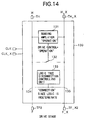
- Figure 10 is a block diagram of a first embodiment of a logic circuit according to the present invention.
- a logic circuit 100 has as main configuration elements, as shown in Fig. 10, an NMOS dual-rail type logic tree portion 110, an SR latch unit 120, and a sensing latch unit 130 including a sense amplifier.
- NMOS dual-rail type logic tree portion 110 when assuming that the input signals of the logical function are A1, A2,... , An and are given together with their inverted signals A1_X, A2_X.... , An_X, one of the logic tree ends TF and TF_X always has a path reaching the ground, and the other always becomes the high impedance state.
- NMOS dual-rail type logic tree portion 110 satisfies such a property, its method of realization is not critical, but it may be configured as shown in for example Fig. 11.
- NMOS dual-rail type logic tree portion 110 of Fig. 11 shows the case of 4 inputs A, B, C, and D and has NMOS transistors NT1101 to NT1112.
- the NMOS transistors NT1101, NT1107, and NT1111 are connected in series between a logical function output node TF I and the ground.
- NMOS transistors NT1104, NT1106, NT1110, and NT1112 are connected in series between a logical function output node TF_X1 and the ground.
- the NMOS transistor NT1102 is connected between the logic output node TF_X1 and the connection point of the NMOS transistors NT1101 and NT1107, and the NMOS transistor NT1103 is connected between the logic output node TF1 and the connection point of the NMOS transistors NT1104 and NT1106.
- an inverted signal A_X obtained by inverting the signal A at an inverter FNV101 is supplied to the gates of the NMOS transistors NT1101 and NT1104, while the signal A is supplied to the gates of the NMOS transistors NT1102 and NT1103.
- the NMOS transistor NT1105 is connected between the connection point of the NMOS transistors NT1101 and NT1107 and the connection point of the NMOS transistors NT1106 and NT1110.
- an inverted signal D_X obtained by inverting the signal D at an inverter INV102 is supplied to the gate of the NMOS transistor NT1105, while the signal D is supplied to the gate of the NMOS transistor NT1106.
- the NMOS transistor NT1108 is connected between the connection point of the NMOS transistors NT1106 and NT1110 and the connection point of the NMOS transistors NT1107 and NT1111, while the NMOS transistor NT1109 is connected between the connection point of the NMOS transistors NT1101 and NT1107 and the connection point of the NMOS transistors NT1110 and NT1112.
- an inverted signal C_X obtained by inverting the signal C at an inverter 1NV103 is supplied to the gates of the NMOS transistors NT1107 and NT1110, while the signal C is supplied to the gates of the NMOS transistors NT1108 and NT 1109.
- an inverted signal B_X obtained by inverting the signal B at an inverter INV104 is supplied to the gate of the NMOS transistor NT1111, while the signal B is supplied to the gate of the NMOS transistor NT1112.
- the SR latch unit 120 receives the logic output H from the output node TH of the sensing latch unit 130 at its set (S) terminal, receives the logic output H_X from the output node TH_X of the sensing latch unit 130 at its reset (R) terminal, holds the logic output of the sensing latch unit 130, and outputs the data from the Q output.
- the SR latch unit 120 has the function of a set and reset latch such as realized generally by two NAND gates or two NOR gates, the method of realization is not critical.
- the polarity of the sensing latch unit 130 indicates the difference of whether the voltage output in the idle stage (flip-flop operation initial state) as will be mentioned later is the logic "1" or the logic "0" for both of the nodes TH and TH_X.
- the SR latch 120 is realized by two NOR gates NR121 and NR122.
- the sensing latch unit 130 has, as shown in Fig. 12, a sense amplifier 131 operating under drive control, a switch 132 serving as the first switching means for short-circuiting the nodes TH and TH_X for the logic outputs H and H_X by this drive control, a logic tree disconnection controlling unit 133, a switch 134 serving as the second switching means for short-circuiting the node TH and the logic input use node TF2 and the node TH_X and the logic input use node TF_X under the control by the logic tree disconnection controlling unit 133, and a switch 135 serving as the third switching means as the main contiguration elements.
- the drive control referred to here indicates the clock signal (synchronization signal) CLK and the inverted signal CLK_X thereof.
- the method of realization of the NMOS dual-rail type logic tree portion 110 and the SR latch unit 120 is not defined very finely.
- the biggest characteristic feature of the present invention resides in the sensing latch unit 130.
- the operation of the sensing latch unit 130 can be divided into the three stages of the "idle stage”, "drive stage”, and the "final determination stage".
- the idling of the operation is indicated by the clock signal CLK and the inverted signal CLK_X thereof, and the sense amplifier 131 does not have a driving capability and does not interfere with the potentials of the nodes TH and TH_X.
- the switch 132 short-circuits the nodes TH and TH_X.
- the logic tree disconnection controlling unit 133 indicates connection to the switches 134 and 135.
- the nodes TH and TF2 and the nodes TH_X and TF_X2 are short-circuited.
- the time where the logic values on the nodes TH and TH_X are not finally determined means the state where the potentials of the nodes H and H_X are equal, or, even if they are different, the difference is small, so the logic values are not clear.
- the switch 132 becomes OFF and cuts off the nodes TH and TH_X, while the sense amplifier 131 has a driving capability and interferes with the potentials of the nodes TH and TH_X to try to make one of them the logic "0" and make the other one the logic "1".
- the logic tree disconnection controlling unit 133 indicates connection with respect to the switches 134 and 135 and short-circuits the nodes TH and TF2 and the nodes TH_X and TF_X2.
- interference occurs between the sense amplifier 131 and the logic tree nodes TF1 and TF_X1.
- One of the logic tree nodes TF1 and TF_X1 always has a path reaching the ground and tries to pull down one of the nodes TH and TH_X to the logic 0.
- the potentials of the nodes TH and TH X which had been the same, start to change in different directions.
- the sense amplifier 131 has a driving capability, and the switch 132 has become OFF, so the potentials of the nodes TH and TH_X are stably maintained.
- the logic tree disconnection controlling unit 133 indicates disconnection to the switches 134 and 135.
- the logic tree 110 and the sense amplifier 131 are electrically cut off in the final determination stage, so are not affected. Furthermore, the insertion to the SR latch is carried out at approximately the same timing as the time when the logic tree disconnection controlling unit 133 indicates disconnection.
- the logic values of the nodes TH and TH_X are stably maintained. Even if the circuit enters the idle stage thereafter, the SR latch unit 120 is in the hold mode, so continuously maintains that value.
- the nodes TH and TH_X output the logic "0" in the idle stage. Furthermore, it is assumed that the sensing latch unit is used in a manner by which the grounding of the logic tree is not suppressed as in Fig. 10.
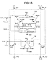
- Figure 16 is a circuit diagram of a first concrete example of a sensing latch unit according to the present invention.
- This sensing latch unit 130A has, as shown in Fig. 16, PMOS transistors PT1301 to PT1304, NMOS transistors NT1301 to NT1307, a first logic input node TF2, second logic input node TF_X2, a first logic output node TH, a second logic output node TH_X, and clock input terminals TCLK and TCLKX.
- the source of the PMOS transistor PT1301 is connected to the supply line of the power source voltage V DD , while the drain is connected to the sources of the PMOS transistors PT1302 and PT1303.
- the drains and gates of the PMOS transistor PT1302 and the NMOS transistor NT1301 are connected to each other to configure an inverter INV131.
- An output node ND131 of the inverter INV131 is configured by the connection point of the drains of the PMOS transistor PT1302 and the NMOS transistor NT1301, while an input node ND132 of the inverter INV131 is configured by the connection point of the gates.
- the drains and gates of the PMOS transistor PT1303 and the NMOS transistor NT1302 are connected to each other to configure an inverter INV132.
- An output node ND133 of the inverter INV132 is configured by the connection point of the drains of the PMOS transistor PT1303 and the NMOS transistor NT1302, while an input node ND134 of the inverter INV132 is configured by the connection point of the gates.
- the sources of the NMOS transistors NT1301 and NT1302 are grounded.
- the output node ND131 of the inverter INV131 is connected to the input node ND134 of the inverter 1NV132 and the logic output terminal TH. while the output node ND133 of the inverter INV132 is connected to the input node ND132 of the inverter INV131 and the logic output terminal TH_X.
- the sense amplifier 131 is configured by the PMOS transistors PT1301 to PT1303 and NT1301 and NT1302 having the above connection relationships.
- This NMOS transistor NT1303 acts as the switch 132.
- the NMOS transistor NT1304 is connected between the logic output node TH and the logic input node TF2, and the NMOS transistor NT1305 is connected between the logic output node TH_X and the logic input node TF_X2.
- NMOS transistor NT1304 acts as the switch 134
- NMOS transistor NT1305 acts as the switch 135.
- the sources of the NMOS transistors NT1306 and NT1307 are grounded, while the drains of them are commonly connected to the gates of the NMOS transistors NT1304 and NT1305 and the drain of the PMOS transistor PT1304. Furthermore, the source of the PMOS transistor PT1304 is connected to the supply line of the power source voltage V DD .
- the logic tree disconnection controlling unit 133 is configured by these PMOS transistor PT1304 and NMOS transistors NT1306 and NT1307.
- the first setting means is configured by the PMOS transistor PT1304, and the second setting means is configured by the NMOS transistors NT1306 and NT1307.
- the gate of the PMOS transistor PT1301, and the gate of the NMOS transistor NT1303 serving as the switch 132 are connected to the clock output terminal TCLKX, while the gate of the PMOS transistor PT1304 is connected to the clock output terminal TCLK.
- the gate of the NMOS transistor NT1306 is connected to the connection point of the logic output terminal TH and the NMOS transistor NT1304, while the gate of the NMOS transistor NT1307 is connected to the connection point of the logic output terminal TH_X and the NMOS transistor NT1305.
- the sensing latch unit 130A having the configuration of Fig. 16, in the idle stage, the clock signal CLK has the logic "0", while the clock inverted signal CLK_X has the logic "1". Accordingly, the PMOS transistor PT1301 becomes cut off and shuts off the current with respect to the sense amplifier 131 part, so the sense amplifier 131 does not have any driving capability.
- the PMOS transistor PT1304 of the logic tree disconnection controlling unit 133 becomes ON and supplies a charge to the control node G.
- the logic potentials of the nodes TH and TH_X are "0", so the NMOS transistors NT1306 and NT1307 have become cut off.
- control node G is initialized to the potential of the logic "1".
- the NMOS transistor NT1303 serving as the switch 132 becomes ON by the clock inverted signal CLK_X, while the NMOS transistor NT1304 serving as the switch 134 and the NMOS transistor NT1305 serving as the switch 135 are controlled by the potential of the control node G and become ON.
- the nodes TH, TH_X, TF2, and TF_X2 are all short-circuited.
- one of the nodes TF1 and TF_X1 of the logic tree always has a path reaching the ground, so the potentials of these nodes TH, TH_X, TF2, and TF_X2 are fixed to the potential of the complete logic "0".
- the PMOS transistor PT1301 becomes ON, the NMOS transistor NT1303 becomes cut off, and the sense amplifier 131 has a driving capability.
- the PMOS transistor PT1304 becomes cut off and the supply of the charge to the control node G is cut off.
- the potentials of the nodes TH and TH_X are the complete logic "0", and the NMOS transistors NT1306 and NT1307 have become cut off.
- one of the nodes TH and TH_X becomes the logic "1".
- the NMOS transistor NT1307 of the logic tree disconnection controlling unit 133 becomes ON and drains the charge on the control node G, whereby the potential of the control node G becomes the complete logic "0".
- the NMOS transistor NT1304 serving as the switch 134 and the NMOS transistor NT1305 serving as the switch 135 become cut off, and the sense amplifier 131 and the logic tree are cut off.
- the NMOS transistor NT1303 serving as the switch 132 becomes ON, and the charges on the nodes TH and TH_X are balanced in distribution.
- the gates and drains of the NMOS transistors NT1301 and NT1302 are short-circuited and these become equivalent to diodes.
- the potentials of the nodes TH and TH_X are quickly pulled down to the vicinity of the threshold value of the NMOS transistor.
- NMOS transistors NT1306 and NT 1307 become cut off.
- the NMOS transistor NT1304 serving as the switch 134 and the NMOS transistor NT1305 serving as the switch 135 become ON, and the sense amplifier 131 and the logic tree are connected again.
- the charges existing on the nodes TH and TH_X and setting the potentials in the vicinity of the NMOS threshold value are pulled out to the ground through the logic tree 110.
- Figure 17 is a circuit diagram of a second concrete example of a sensing latch unit according to the present invention.
- this sensing latch unit 130B differs from the sensing latch unit 130A of Fig. 16 resides in the fact that an NMOS transistor NT1308 is connected between the intermediate node MG serving as the connection point of the sources of the NMOS transistors NT1306 and NT1307 in the logic tree disconnection controlling unit and the ground, and the gate of this NMOS transistor NT1308 is connected to the clock input terminal TCLK.
- Figure 18 is a circuit diagram of a third concrete example of a sensing latch unit according to the present invention.
- sensing latch unit 130C The difference of this sensing latch unit 130C from the sensing latch units 130A and 130B of Fig. 16 and Fig. 17 resides in the fact that the logic tree disconnection controlling unit has a static NOR logic circuit configuration in place of the dynamic NOR logic circuit configuration.
- the supply line of the power source voltage V DD and the control node G are connected by two serially connected PMOS transistors PT1305 and PT1306 in place of the precharge use PMOS transistor PT1304, the gate of the PMOS transistor PT1305 is connected to the logic output node TH, the gate of the PMOS transistor PT1306 is connected to the logic output node TH_X, and the logic tree disconnection controlling circuit is configured by the static NOR circuit S-NOR.
- the potential of the control node G is determined and the cut off of the logic tree is controlled not depending upon the clock signal (synchronization signal) CLK viewing the logic potentials of the nodes TH and TH_X.
- both of the nodes TH and TH_X have the logic "0", therefore the control node G is set to the logic "1".
- the control node G is made the logic "0".
- the advantage of the present third concrete example over the first and second concrete examples resides in the fact that the logic tree disconnection controlling unit does not need the clock signal (synchronization signal) CLK, so the additions for the clock signal (synchronization signal) CLK are reduced.
- the glitches in the static CMOS logic circuit were taken up as the problem of the conventional example.
- a SPICE simulation was carried out by using the logical function and input signal patterns (those in which A, B, C, and D change at a variety of timings) used as the example at this time.
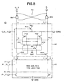
- Figure 19 is a view of current waveforms in the conventional CMOS logic circuit shown in Fig. 4 and the logic circuit according to the present invention.
- an abscissa represents the time, and an ordinate represents the current and the voltage.
- the characteristic curve indicated by a solid line is the current waveform of the circuit of the present invention, while the characteristic curve indicated by a broken line is the current waveform of the conventional circuit.
- the logic circuit operates whenever a change occurs in the input signal and current is consumed.
- the circuit of the present invention has realized a reduction of the power consumption in comparison with the conventional circuit.
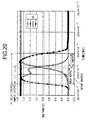
- Figure 20 is a view of an operation delay characteristic of the static CMOS logic circuit
- Fig. 21 is a view of the operation delay characteristic of the logic circuit of the present invention.
- all of the input signals of the logical function have a set-up time and hold time with respect to the clock signal (synchronization signal) CLK.
- the particularly important signals are the signal which is transferred to the logical function output F fastest and the signal transferred slowest.
- the synchronization timings with respect to the clock signal (synchronization signal) CLK are different. For this reason, there are cases where the set-up time and the hold time become negative. This makes this unsuitable for comparison. Accordingly, it is better for the comparison if the sum of the set-up time and the hold time is defined as the sample time (Sample in the figure) and the sum of the set-up time and Tcq is defined as the delay time (FFDelay in the figure).
- sample time just means the time of sampling the input signals not permitting a change of the input signal.
- the “delay time” means the time which is consumed by the flip-flop and the logical function part in one cycle. In both of them, the shorter the time, the better the performance.
- the sample time becomes 427 ps in the conventional circuit as shown in Fig. 20, while becomes 711 ps in the circuit of the present invention as shown in Fig. 21.
- the first object of the present invention that is, the elimination of glitches to reduce the power consumption and the realization of high speed operation by making good use of the characteristics of the dynamic logic circuit, was achieved.
- the second object of the present invention was the eliminate the mechanism for generating a pulse having a short width as in the PDN-F/F logic circuit and facilitating design by the automatic placement and routing by CAD.
- the sensing latch unit 130 and the NMOS dual-rail type logic tree portion 110 are employed.
- the problem of the SA-F/F logic circuit resides in that the time required for the final determination of the logic definition closely depended upon the height of the logic tree and the size of the MOS transistors in the logic tree.
- the height of the logic tree represents the number of input signals of the logical function, the more complex the logical function, the larger the time for final determination of the logic.
- Figure 22 is a view of the characteristic of the Tcq versus the height of the logic tree in the SA-F/F logic circuit and the circuit of the present invention
- Fig. 23 is a view of the characteristic of the Tcq versus the logic tree NMOS size (Wn) in the SA-F/F logic circuit and the circuit of the present invention.
- the abscissa represents the height of the logic tree, and the ordinate represents the Tcq
- the abscissa represents the NMOS size of the logic tree
- the ordinate represents the Tcq fluctuation rate
- the black marks indicate the characteristic of the SA-F/F logic circuit
- the white marks and x marks indicate the characteristics of the circuit of the present invention.
- the dependency of the Tcq on the height of the logic tree is smaller in the circuit of the present invention. As the logic tree becomes higher, the circuit of the present invention operates at a higher speed.
- Fig. 23 specifically shows the rate of fluctuation of the Tcq when the size Wn of the NMOS transistor in the logic tree is changed from 0.64 ⁇ m to 0.36 ⁇ m.
- the height of the logic tree at this time is 5.
- the potentials of the nodes in the sense amplifier and the nodes of the logic tree start from the potential of the logic "1" or the potential near this and are pulled down to the potential of the complete logic "0".
- the height of the logic tree is not that relevant to the boosting of the potential.
- the superiority of the circuit of the present invention over an SA-F/F logic circuit when realizing a complex logical function is clear.
- the object of the present invention that is, the realization of high speed operation even in the case of realizing a complex logical function having many input signals, was achieved.
- the fourth object of the present invention was the realization of an operation resistant to variations of the circuit constant and coupling noise and stabler than that by a DCSL circuit.
- One of the causes for the susceptibility of the DCSL circuit to incorrect potential fluctuations is the fact that the voltage applied to the gate terminal of the switch comprising the NMOS transistors performing the connection and disconnection of the logic tree and the sense amplifier is low, i.e., about the threshold value of the NMOS transistor.
- connection and the disconnection of the logic tree 110 and the sense amplifier 131 are carried out by the control node G in the sensing latch unit 130.
- the charge is supplied by the PMOS transistor, and the potential of the complete logic "1" is given.
- the NMOS transistors NT1304 and NT1305 serving as the switches 134 and 135 become sufficiently ON, have small conduction resistances, and can easily absorb incorrect potential fluctuation.
- the potentials added to the gate terminals of the NMOS transistors serving as the switches are different nodes.
- the node TH_X is connected to the gate terminal of the NMOS transistor NT43, while the node TH is connected to the gate terminal of the NMOS transistor NT44.
- the turning ON and OFF of the NMOS transistors NT1304 and NT1305 serving as the switches 134 and 135 are controlled by the common control node G.
- Figure 24 is a view of the process by which the sensing latch unit according to the present invention absorbs the incorrect potential fluctuation and the correct logic value is finally set to.
- Figure 24 concretely shows the situation where noise lowering the potential of the node TH is given in the process by which the node TH is finally determined as the original logic "1".
- the sense amplifier and the logic tree are connected, and all of nodes in the sense amplifier and the nodes of the logic tree are short-circuited and initialized to the same potential.
- the first embodiment is configured provided with the NMOS dual-rail type logic tree portion 110 in which when the input signal of the logical function is given, one of the logic tree ends TF and TF_X always has a path reaching the ground and the other always becomes a high impedance state
- the SR latch unit 120 which receives at its set (S) terminal the logic output H from the output node TH of the sensing latch unit 130 and receives at its reset (R) terminal the logic output H_X from the output node TH_X of the sensing latch unit 130, holds the logic output of the sensing latch unit 130, and outputs the data from the Q output, and the sensing latch unit 130 having the sense amplifier 131 operating by the drive control, the switch 132 for short-circuiting the nodes TH and TH_X for the logic outputs H and H_X by this drive control, the logic tree disconnection controlling unit 133, and the switches 134 and 135 which are controlled by the logic tree disconnection controlling unit 133 and short-circuit the node
- the glitches occurring in the static CMOS logic circuit are eliminated to reduce the power consumption and high speed operation can be realized by making good use of the characteristics of the dynamic logic circuit.
- the mechanism for generating a pulse having a short width such as a PDN-F/F logic circuit is eliminated and design by automatic placement and routing by CAD can be facilitated.
- the dependency of the operating speed on the height of the logic tree and the gate width of the MOS in the logic tree is made smaller than that of the SA-F/F logic circuit, and high speed operation can be realized even in the case of realizing a complex logical function having many input signals.
- Figure 25 is a block diagram of a second embodiment of a logic circuit according to the present invention
- Fig. 26 is a circuit diagram of an example of the concrete configuration of an NMOS dual-rail type logic tree portion and an SR latch unit in the logic circuit of Fig. 25.
- the difference of the second embodiment from the first embodiment resides in that an NMOS transistor NT101 controlling the grounding of the NMOS dual-rail type logic tree 110 in synchronization with the synchronization signal (clock signal) is added.
- This NMOS transistor NT101 becomes cut off in the initial state of the operation of the flip-flop.
- the NMOS transistor NT101 becomes ON when the clock signal (synchronization signal) CLK has the logic "1"
- the sensing latch unit 130 itself to have the function of pulling down the potentials of the nodes TH and TH_X to the vicinity of the threshold value of the NMOS transistor and turn ON the NMOS transistor NT1304 serving as the switch 134 and the NMOS transistor NT1305 serving as the switch 135 connecting the logic tree 110 and the sense amplifier 131.
- the potentials of the nodes TH, TH_X, TF, and TF_X become values a little smaller than the threshold value of the NMOS transistor, but a little larger than the potential of the complete logic "0".
- the advantage of the second embodiment over the first embodiment resides in the reduction of the power consumption and the increase of the speed.
- part of the charge supplied in the drive stage is preserved and reused in the next drive stage. For this reason, the power consumption can be reduced more.
- the potentials of the nodes TH and TH_X rise starting from the potential near the threshold value of the NMOS transistor, therefore the time required for the final determination of the logic becomes shorter than that of the configuration of Fig. 10 in which the potential starts to rise from the potential of the complete logic "0".
- Figure 27 is a block diagram of a third embodiment of a logic circuit according to the present invention
- Fig. 28 is a circuit diagram of an example of the concrete configurations of the NMOS dual-rail type logic tree portion and the SR latch unit in the logic circuit of Fig. 27.
- the difference of the third embodiment from the second embodiment resides in that an NMOS transistor NT102 for controlling the grounding of the NMOS dual-rail type logic tree in synchronization with the control signal SLEEP different from the clock signal (synchronization signal) is connected in parallel to the NMOS transistor NT101.
- the NMOS transistor NT102 becomes cut off when the control signal SLEEP has the logic "0".
- the operation at this time is the same as that of Fig. 26 according to the second embodiment.
- control signal SLEEP the logic "1" occurs when the clock signal (synchronization signal) CLK stops at the logic "0".
- the stopped clock becomes constant at the logic "0” or the logic "1". Which value it becomes constant at differs according to the design, but once designed, the clock always stops at the same logic value.
- the nodes TH and TH_X become potentials a little lower than the threshold value of the NMOS transistor.
- the SR latch unit 120 receives this as the logic "0" and operates as the hold mode. There is no logical problem.
- the NMOSs having the nodes TH and TH_X at their gate terminals in the SR latch unit 120 are in the cut off state at this time.
- the MOS passes a current though the amount is extremely small even in the cut-off state. This will be referred to as the leakage current.
- the magnitude of the leakage current is determined by an exponential function of the gate terminal potential. Accordingly, in the magnitude of the leakage current between the case where the potentials of the nodes TH and TH_X are complete 0V and the case where they have values near the threshold value of the NMOS transistor, there is a difference of about one order to two orders though the absolute value thereof is small.
- the power consumption can be made smaller in the case where the charges for reuse are discarded and the potentials of the nodes TH and TH_X are dropped to the potential of the complete logic "0".
- Figure 29 is a view of the potential waveforms of the internal nodes TH and TH_X at the time of the SLEEP mode operation and the simulation results of the leakage current value.
- control signal SLEEP is still at the logic "0". Accordingly, the nodes TH and TH_X do not have potentials of the complete logic "0".
- the leakage current during the illustrated period is 557.3 nA.
- the mechanism for generating a pulse having a short width such as a PDN-F/F logic circuit is eliminated and design by automatic placement and routing by CAD can be facilitated.
- the dependency of the operating speed on the height of the logic tree and the gate width of the MOS in the logic tree is made smaller than that of the SA-F/F logic circuit, and high speed operation can be realized even in the case of realizing a complex logical function having many input signals.
- the leakage current can be reduced.
Landscapes
- Logic Circuits (AREA)
- Electronic Switches (AREA)
Applications Claiming Priority (2)
| Application Number | Priority Date | Filing Date | Title |
|---|---|---|---|
| JP36566499A JP2001186009A (ja) | 1999-12-22 | 1999-12-22 | 論理回路 |
| JP36566499 | 1999-12-22 |
Publications (1)
| Publication Number | Publication Date |
|---|---|
| EP1111615A1 true EP1111615A1 (en) | 2001-06-27 |
Family
ID=18484821
Family Applications (1)
| Application Number | Title | Priority Date | Filing Date |
|---|---|---|---|
| EP00400539A Withdrawn EP1111615A1 (en) | 1999-12-22 | 2000-02-29 | Logic circuit |
Country Status (6)
| Country | Link |
|---|---|
| US (1) | US6374393B1 (https=) |
| EP (1) | EP1111615A1 (https=) |
| JP (1) | JP2001186009A (https=) |
| KR (1) | KR100613738B1 (https=) |
| CN (1) | CN1175421C (https=) |
| TW (1) | TW463166B (https=) |
Cited By (2)
| Publication number | Priority date | Publication date | Assignee | Title |
|---|---|---|---|---|
| WO2004019492A3 (en) * | 2002-08-23 | 2004-11-04 | Sun Microsystems Inc | Clocked full-rail differential logic with sense amplifier and shut-off |
| DE102004037591A1 (de) * | 2004-08-03 | 2006-03-16 | Infineon Technologies Ag | Dual-Rail Precharged Flip-Flop |
Families Citing this family (23)
| Publication number | Priority date | Publication date | Assignee | Title |
|---|---|---|---|---|
| DE10022263A1 (de) * | 2000-05-08 | 2001-11-22 | Infineon Technologies Ag | Speicher-Leseverstärker |
| US6557149B2 (en) * | 2001-04-04 | 2003-04-29 | Intel Corporation | Algorithm for finding vectors to stimulate all paths and arcs through an LVS gate |
| DE10217375B4 (de) * | 2002-04-18 | 2006-08-24 | Infineon Technologies Ag | Schaltungsanordnung und Verfahren zur Erzeugung eines Dual-Rail-Signals |
| US6886152B1 (en) * | 2002-08-09 | 2005-04-26 | Xilinx, Inc. | Delay optimization in signal routing |
| US7131092B2 (en) * | 2004-12-21 | 2006-10-31 | Via Technologies, Inc. | Clock gating circuit |
| JP4859370B2 (ja) * | 2005-01-19 | 2012-01-25 | 三菱電機株式会社 | 電子素子 |
| US7302659B2 (en) * | 2005-02-10 | 2007-11-27 | International Business Machines Corporation | System and method for unfolding/replicating logic paths to facilitate propagation delay modeling |
| US7447620B2 (en) * | 2006-02-23 | 2008-11-04 | International Business Machines Corporation | Modeling asynchronous behavior from primary inputs and latches |
| US7437584B2 (en) * | 2006-02-27 | 2008-10-14 | Atmel Corporation | Apparatus and method for reducing power consumption in electronic devices |
| US7490305B2 (en) * | 2006-07-17 | 2009-02-10 | International Business Machines Corporation | Method for driving values to DC adjusted/untimed nets to identify timing problems |
| US7882473B2 (en) * | 2007-11-27 | 2011-02-01 | International Business Machines Corporation | Sequential equivalence checking for asynchronous verification |
| US20090167395A1 (en) * | 2007-12-31 | 2009-07-02 | Texas Instruments Incorporated | High performance latches |
| US7861200B2 (en) * | 2008-03-24 | 2010-12-28 | Freescale Semiconductor, Inc. | Setup and hold time characterization device and method |
| US8122410B2 (en) * | 2008-11-05 | 2012-02-21 | International Business Machines Corporation | Specifying and validating untimed nets |
| US20110016367A1 (en) * | 2009-07-14 | 2011-01-20 | Bo Tang | Skew tolerant scannable master/slave flip-flop including embedded logic |
| KR20110105153A (ko) * | 2010-03-18 | 2011-09-26 | 삼성전자주식회사 | 플립플롭 회로 및 스캔 플립 플롭 회로 |
| US8975949B2 (en) * | 2013-03-14 | 2015-03-10 | Samsung Electronics Co., Ltd. | Integrated clock gater (ICG) using clock cascode complimentary switch logic |
| US9256245B2 (en) * | 2014-04-02 | 2016-02-09 | Mediatek Inc. | Clock tree circuit and memory controller |
| KR20160005535A (ko) * | 2014-07-07 | 2016-01-15 | 에스케이하이닉스 주식회사 | 반도체 장치의 리시버 회로 |
| TWI705666B (zh) * | 2015-06-15 | 2020-09-21 | 日商新力股份有限公司 | 傳送裝置、接收裝置、通信系統 |
| US11658656B2 (en) | 2020-11-26 | 2023-05-23 | Samsung Electronics Co., Ltd. | Low power clock gating cell and an integrated circuit including the same |
| KR20220143272A (ko) | 2021-04-16 | 2022-10-25 | 삼성전자주식회사 | 직렬 스택 구조의 트랜지스터들을 포함하는 플립 플롭 |
| TW202533531A (zh) * | 2023-12-27 | 2025-08-16 | 日商索尼半導體解決方案公司 | 邏輯運算電路 |
Family Cites Families (3)
| Publication number | Priority date | Publication date | Assignee | Title |
|---|---|---|---|---|
| US6002270A (en) * | 1995-11-09 | 1999-12-14 | Spaceborne, Inc. | Synchronous differential logic system for hyperfrequency operation |
| JPH10269774A (ja) * | 1997-03-26 | 1998-10-09 | Matsushita Electric Ind Co Ltd | 半導体記憶装置 |
| KR100434965B1 (ko) * | 1997-12-29 | 2004-07-16 | 주식회사 하이닉스반도체 | 센스앰프 구동장치 |
-
1999
- 1999-12-22 JP JP36566499A patent/JP2001186009A/ja not_active Abandoned
-
2000
- 2000-02-24 TW TW089103242A patent/TW463166B/zh not_active IP Right Cessation
- 2000-02-28 US US09/514,256 patent/US6374393B1/en not_active Expired - Fee Related
- 2000-02-29 KR KR1020000010243A patent/KR100613738B1/ko not_active Expired - Fee Related
- 2000-02-29 CN CNB001083511A patent/CN1175421C/zh not_active Expired - Fee Related
- 2000-02-29 EP EP00400539A patent/EP1111615A1/en not_active Withdrawn
Non-Patent Citations (1)
| Title |
|---|
| SOMASEKHAR D ET AL: "DIFFERENTIAL CURRENT SWITCH LOGIC: A LOW POWER DCVS LOGIC FAMILY", IEEE JOURNAL OF SOLID-STATE CIRCUITS,US,IEEE INC. NEW YORK, vol. 31, no. 7, 1 July 1996 (1996-07-01), pages 981 - 991, XP000632385, ISSN: 0018-9200 * |
Cited By (2)
| Publication number | Priority date | Publication date | Assignee | Title |
|---|---|---|---|---|
| WO2004019492A3 (en) * | 2002-08-23 | 2004-11-04 | Sun Microsystems Inc | Clocked full-rail differential logic with sense amplifier and shut-off |
| DE102004037591A1 (de) * | 2004-08-03 | 2006-03-16 | Infineon Technologies Ag | Dual-Rail Precharged Flip-Flop |
Also Published As
| Publication number | Publication date |
|---|---|
| US6374393B1 (en) | 2002-04-16 |
| KR100613738B1 (ko) | 2006-08-22 |
| CN1175421C (zh) | 2004-11-10 |
| TW463166B (en) | 2001-11-11 |
| JP2001186009A (ja) | 2001-07-06 |
| CN1301023A (zh) | 2001-06-27 |
| KR20010082496A (ko) | 2001-08-30 |
Similar Documents
| Publication | Publication Date | Title |
|---|---|---|
| US6374393B1 (en) | Logic circuit evaluation using sensing latch logic | |
| US6445210B2 (en) | Level shifter | |
| US6023179A (en) | Method of implementing a scan flip-flop using an edge-triggered staticized dynamic flip-flop | |
| US6459316B1 (en) | Flip flop circuit | |
| US7808294B1 (en) | Level shifter with balanced rise and fall times | |
| KR100425474B1 (ko) | 감소된 프리차지 레벨을 적용하는 데이터 출력방법과데이터 출력회로 | |
| US5867049A (en) | Zero setup time flip flop | |
| US6043696A (en) | Method for implementing a single phase edge-triggered dual-rail dynamic flip-flop | |
| CN1964194A (zh) | 具有加速非充电路径的n型多米诺寄存器 | |
| US9806698B1 (en) | Circuit and method for a zero static current level shifter | |
| KR101811019B1 (ko) | 전하-주입 감지 증폭기 논리회로 | |
| US6191618B1 (en) | Contention-free, low clock load domino circuit topology | |
| US7737757B2 (en) | Low power level shifting latch circuits with gated feedback for high speed integrated circuits | |
| US20040155678A1 (en) | Domino logic compatible scannable flip-flop | |
| US6414529B1 (en) | Latch and D-type flip-flop | |
| US6989691B2 (en) | Dynamic to static converter with noise suppression | |
| US8816749B2 (en) | Level shifter device | |
| CN100413073C (zh) | 用于避免多电源输入/输出的瞬态短路电流的集成电路 | |
| US5894227A (en) | Level restoration circuit for pass logic devices | |
| US6396305B1 (en) | Digital leakage compensation circuit | |
| US8063685B1 (en) | Pulsed flip-flop circuit | |
| US7602217B2 (en) | Level shifter circuit with pre-charge/pre-discharge | |
| CN103229417B (zh) | 具有同步数据加载和自定时异步数据俘获的锁存器电路 | |
| US6404253B1 (en) | High speed, low setup time voltage sensing flip-flop | |
| US20080042693A1 (en) | Design structures comprising receiver circuits for generating digital clock signals |
Legal Events
| Date | Code | Title | Description |
|---|---|---|---|
| PUAI | Public reference made under article 153(3) epc to a published international application that has entered the european phase |
Free format text: ORIGINAL CODE: 0009012 |
|
| AK | Designated contracting states |
Kind code of ref document: A1 Designated state(s): DE FR GB |
|
| AX | Request for extension of the european patent |
Free format text: AL;LT;LV;MK;RO;SI |
|
| 17P | Request for examination filed |
Effective date: 20011217 |
|
| AKX | Designation fees paid |
Free format text: DE FR GB |
|
| STAA | Information on the status of an ep patent application or granted ep patent |
Free format text: STATUS: THE APPLICATION IS DEEMED TO BE WITHDRAWN |
|
| 18D | Application deemed to be withdrawn |
Effective date: 20030829 |