EP1111479A1 - Method and apparatus for image formation - Google Patents
Method and apparatus for image formation Download PDFInfo
- Publication number
- EP1111479A1 EP1111479A1 EP00908014A EP00908014A EP1111479A1 EP 1111479 A1 EP1111479 A1 EP 1111479A1 EP 00908014 A EP00908014 A EP 00908014A EP 00908014 A EP00908014 A EP 00908014A EP 1111479 A1 EP1111479 A1 EP 1111479A1
- Authority
- EP
- European Patent Office
- Prior art keywords
- image forming
- image
- photoconductor
- recording medium
- surface potential
- Prior art date
- Legal status (The legal status is an assumption and is not a legal conclusion. Google has not performed a legal analysis and makes no representation as to the accuracy of the status listed.)
- Granted
Links
Images



Classifications
-
- G—PHYSICS
- G03—PHOTOGRAPHY; CINEMATOGRAPHY; ANALOGOUS TECHNIQUES USING WAVES OTHER THAN OPTICAL WAVES; ELECTROGRAPHY; HOLOGRAPHY
- G03G—ELECTROGRAPHY; ELECTROPHOTOGRAPHY; MAGNETOGRAPHY
- G03G21/00—Arrangements not provided for by groups G03G13/00 - G03G19/00, e.g. cleaning, elimination of residual charge
- G03G21/06—Eliminating residual charges from a reusable imaging member
-
- G—PHYSICS
- G03—PHOTOGRAPHY; CINEMATOGRAPHY; ANALOGOUS TECHNIQUES USING WAVES OTHER THAN OPTICAL WAVES; ELECTROGRAPHY; HOLOGRAPHY
- G03G—ELECTROGRAPHY; ELECTROPHOTOGRAPHY; MAGNETOGRAPHY
- G03G15/00—Apparatus for electrographic processes using a charge pattern
- G03G15/20—Apparatus for electrographic processes using a charge pattern for fixing, e.g. by using heat
- G03G15/2003—Apparatus for electrographic processes using a charge pattern for fixing, e.g. by using heat using heat
- G03G15/2007—Apparatus for electrographic processes using a charge pattern for fixing, e.g. by using heat using heat using radiant heat, e.g. infrared lamps, microwave heaters
- G03G15/201—Apparatus for electrographic processes using a charge pattern for fixing, e.g. by using heat using heat using radiant heat, e.g. infrared lamps, microwave heaters of high intensity and short duration, i.e. flash fusing
-
- G—PHYSICS
- G03—PHOTOGRAPHY; CINEMATOGRAPHY; ANALOGOUS TECHNIQUES USING WAVES OTHER THAN OPTICAL WAVES; ELECTROGRAPHY; HOLOGRAPHY
- G03G—ELECTROGRAPHY; ELECTROPHOTOGRAPHY; MAGNETOGRAPHY
- G03G21/00—Arrangements not provided for by groups G03G13/00 - G03G19/00, e.g. cleaning, elimination of residual charge
Definitions
- the present invention relates to an image forming method and an image forming apparatus.
- an electrophotographic image forming apparatus In an electrophotographic image forming apparatus, light is applied to a uniformly charged surface of an image carrier such as a photoconductive drum or a photoconductive belt in accordance with printing information to thereby form an electrostatic latent image, then the electrostatic latent image is developed with toner particles, and then the developed toner image is transferred to a recording medium such as paper or resin film and fixed using heat, pressure, light or the like.
- an image carrier such as a photoconductive drum or a photoconductive belt in accordance with printing information to thereby form an electrostatic latent image
- the electrostatic latent image is developed with toner particles
- the developed toner image is transferred to a recording medium such as paper or resin film and fixed using heat, pressure, light or the like.
- the most general way of fixing the toner image is the way using heat rolls.
- the fixing using heat rolls has the following problems: Though heat efficiency is high, initial heating (rising) takes several minutes. Further, toner is apt to be put out of position onto the heat rolls and stain the recording paper. Further, since the recording medium is nipped by a pair of heat rolls, when the recording medium is continuous paper such as paper for computer output, wrinkles and brakes are apt to be produced due to the paper's meandering.
- toner absorbs radiant energy selectively and enables high-speed fixing. Further, in flash fixing, a flash lamp and recording paper are not in contact. This has an advantage that there is no fear of toner's being put out of position, or wrinkles and brakes being produced due to the recording medium's meandering. Another advantage is that a toner image is fixed easily even to sized paper.
- part of flash light can impinge on the photoconductor as leak light, directly or indirectly, that is, having been reflected by a reflecting plate or shielding plate attached to the flash lamp, a carrying belt, paper and/or the like, in accordance with the flash lamp periodically emitting the flash light, intermittently. This can produce stains on a white ground.
- the flash-lamp side of the carrying belt is exposed between cut sheets. Therefore, for example, if antireflection treatment such as black coating is applied to the carrying belt, it may reduce the leak light from the flash lamp impinging on the photoconductor. However, when continuous paper is used, the carrying belt is not exposed. Therefore, more intensive leak light from the flash lamp may impinge on the photoconductor. In that case, photo fatigue and transfer memory may be produced at those portions of the photoconductor on which the flash light has impinged, so that the capability to be charged may drop.
- antireflection treatment such as black coating
- photo fatigue means that the capability of the photoconductor to be charged drops at its portions that have received intensive light.
- photo fatigue can be evaluated as follows: After electricity is removed from a photoconductor 1 by a discharging lamp 2, the photoconductor 1 is charged by a main charger 3. Then, flash light from a flash lamp 5 is applied to the photoconductor 1 through a slit 4. A decrease in surface potential ⁇ 1 of the surface of the photoconductor 1 caused by the flash lamp 5 being turned on after the main charging (as shown in FIG. 5) is measured with a surface potential sensor 7 to thereby evaluate photo fatigue.
- Transfer memory means, as shown in FIG. 6, that electric charge supplied by a transfer charger 6 having a polarity opposite to the polarity of the photoconductor 1 remains until directly before charging by a main charger 3, so that an increase in surface potential caused by the charging by the main charger 3 reduces, that is, the capability to be charged drops.
- Transfer memory can be evaluated as follows: After electricity is removed from the photoconductor 1 by the dischaging lamp 2, the photoconductor 1 is charged by the main charger 3. Then, the photoconductor 1 is subjected to transfer charging by the transfer charger 6 whose polarity is opposite to the polarity of the main charging. Then, a decrease in surface potential ⁇ 2 of the surface of the photoconductor 1 after the main charging (as shown in FIG. 7) is measured with a surface potential sensor 7 to thereby evaluate transfer memory. A larger decrease in surface potential ⁇ 2 means a larger tendency to produce transfer memory.
- Transfer memory is apt to be produced in reversal development using a transfer charger whose polarity is opposite to the polarity of a photoconductor. Therefore, generally, the capability to be charged drops more in reversal development in which both photo fatigue and transfer memory affect the capability than in normal development in which only photo fatigue affects it.
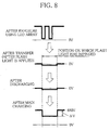
- FIG. 8 shows how the surface potential of the deteriorated photoconductor varies after each step.
- the capability of the photoconductor to be charged drops at its portions that have received flash light. Portions that have a lower surface potential after main charging are produced in accordance with the flash light being emitted periodically. If a decrease in surface potential ⁇ V is large, it may cause stains on a white ground in reversal development and decrease in concentration in normal development.
- the present invention has been made in view of the above problems.
- the object of the present invention is to provide an image forming method and image forming apparatus in which a recording medium is carried well and the possibility of producing stains on a white ground is low even if flash light impinges on an image carrier.
- the present invention provides an image forming method in which a toner image formed on an image carrier through steps of discharging, main charging, exposure and development is transferred to a recording medium and then fixed as an image using flash light, wherein after the toner image is transferred, the image carrier is subjected, prior to discharging, to secondary charging that gives the same polarity as the main charging gives and a surface potential larger in absolute value than the main charging gives.
- the recording medium is continuous paper.
- a carrying path along which the recording medium is carried while the toner image is transferred and then fixed is substantially a straight line.
- the development through which the toner image is formed is reversal development.
- the image carrier is an organic photoconductor.
- the flash light is emitted from a plurality of light sources simultaneously.
- the present invention provides an image forming apparatus comprising at least an image carrier, main charging means, exposure means, development means, transfer means for transferring an image to a recording medium, discharging means, fixing means using a flash lamp, carrying means for carrying the recording medium from transfer position to fixing position, and secondary charging means for secondarily charging the image carrier to have the same polarity as a polarity given by the main charging means and a surface potential larger in absolute value than a surface potential given by the main charging means, the secondary charging means being arranged to act on the image carrier after the transfer means acts on the image carrier and before the discharging means acts on the image carrier.
- the recording medium is continuous paper.
- the carrying means carries the recording medium along a carrying path that is substantially a straight line.
- the development means is means for performing reversal development.
- the image carrier is an organic photoconductor.
- the fixing means comprises a plurality of flash lamps adapted to emit light simultaneously.
- FIG. 1 shows a schematic structure of an electrophotographic printer to which an image forming method and image forming apparatus of the present invention is applied;
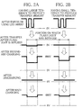
- FIGS. 2A and 2B show how the surface potential of a photoconductor of the electrophotographic printer of FIG. 1 varies after each step;
- FIG. 3 shows another form of the electrophotographic printer shown in FIG. 1;
- FIG. 4 is a diagram for use in explaining photo fatigue of a photoconductor;
- FIG. 5 is a diagram for use in explaining the way of evaluating photo fatigue of a photoconductor;
- FIG. 6 is a diagram for use in explaining transfer memory of a photoconductor;
- FIG. 7 is a diagram for use in explaining the way of evaluating transfer memory of a photoconductor; and
- FIG. 8 shows how the surface potential of a deteriorated photoconductor varies after each step.
- the electrophotographic printer 10 comprises a main charger 12, an LED array 13, a developer unit 14, a transfer charger 15, a separate charger 16, a secondary charger 17, a cleaner 18 and a discharging lamp 19 which are arranged around a photoconductor 11.
- the electrophotographic printer 10 further comprises a tractor 20 that provides a carrying-in path along which paper S is carried to the transfer charger 15, a carrying belt 21 that provides a carrying-out path along which paper S is carried from the separate charger 16, and a shielding plate 22, a flash lamp 23 and a reflector 24 which are arranged opposite to the carrying belt 21.
- the photoconductor 11 is a positively-charged single-layer type organic photoconductor, for example, Marine-2 manufactured by Mita Kogyo Kabushiki Kaisha.
- organic photoconductive pigments are desirable.
- phthalocyanine pigment, perylene pigment, quinacridon pigment, pyranthrone pigment, bis-azo pigment, tri-azo pigment and the like can be mentioned.
- One of those organic photoconductive pigments may be used singly, or two or more of those organic photoconductive pigments may be used together.
- a charge transporting medium can be prepared by having charge transporting material dispersed in binding resin.
- charge transporting material any hole transporting substance or electron transporting substance that a person skilled in the art usually uses may be used.
- phenylendiamine compounds such as N,N,N',N'-tetrakis(3-methylphenyl)-m-phenylenediamine, poly-N-vinylcarbazole, phenanthrene, N-ethylcarbazole, 2,5-diphenyl-1,3,4-oxadiazole, 2,5-bis(4-diethylaminophenyl)-1,3,4-oxadiazole, bis-diethylaminophenyl-1,3,6-oxadiazole, 4,4'-bis(diethylamino)-2,2'-dimethyltriphenylmethane, 2,4,5-triaminophenylimidazole, 2,5-bis(4-diethylaminophenyl)-1,3,4-triazole, 1-phenyl-3-(4-diethylaminostyryl)-5-(4-diethylaminophenyl)-2-pyrazoline,
- phenoquinones such as 3,5,3',5'-tetraphenyldiphenoquinone, 2-nitro-9-fluorenone, 2,7-dinitro-9-fluorenone, 2,4,7-trinitro-9-fluorenone, 2,4,5,7-tetranitro-9-fluorenone, 2-nitrobenzothiophene, 2,4,8-trinitrothioxanthone, dinitroanthracene, dinitroacridine, dinitroanthoquinone and the like can be mentioned.
- One of those substances may be used singly, or two or more of those substances may be used together.
- binding resin various polymers can be enumerated such as styrene polymer, styrene-butadiene copolymer, styreneacrylonitrile copolymer, styrene-maleic acid copolymer, acrylic polymer, styrene-acrylic copolymer, styrene-vinyl acetate copolymer, polyvinyl chloride, vinyl chloride-vinyl acetate copolymer, polyester, alkyd resin, polyamide, polyurethane, epoxy resin, polycarbonate, polyarylate, polysulfone, diarylphthalate resin, silicone resin, ketone resin, polyvinylbutyral resin, polyether resin, phenolic resin; and photo-curing resins such as epoxyacrylate, urethaneacrylate and the like.
- Photoconductive polymers such as poly-N-vinylcarbazole and the like can also be used as binding resin.
- a negatively-charged laminated organic photoconductor may be used.
- phthalocyanine pigment, anthoanthorone pigment, dibenzpyrene pigment, pyranthrone pigment, azo pigment, indigo pigment, quinacridon pigment, pyrylium dye, thiapyrylium dye, xanthene pigment, quinoneimine pigment, triphenylmethane pigment, styryl pigment and the like can be mentioned as charge producing materials.
- Charge producing materials are not limited to those mentioned above.
- One kind of charge producing material may be used singly, or two or more kinds of charge producing materials may be mixed together and used.
- a charge transporting layer can be formed by applying the charge transporting material as mentioned above on a substrate, if necessary, together with suitable binder. (Binder is not always needed.)
- the mean particle diameter of charge producing material in its dispersed state is desirably not larger than 3 ⁇ m, more desirably not larger than 1 ⁇ m.
- the manner of applying the material can be dip coating, spray coating, spinner coating, bead coating, wire bar coating, blade coating, roller coating, curtain coating or the like.
- the charge transporting layer is electrically connected with a charge producing layer.
- the charge transporting layer has a function of receiving charge carriers injected from the charge producing layer under the influence of an electric field and transporting those charge carriers.
- the charge transporting layer is formed on the charge producing layer.
- the charge transporting layer is formed by applying a coat of organic charge transporting material such as a hydrazone compound, a pyrazoline compound, a stilbene compound, an oxazole compound, a thiazole compound, a triarylmethan compound or the like, if necessary, together with binder resin.
- organic charge transporting material such as a hydrazone compound, a pyrazoline compound, a stilbene compound, an oxazole compound, a thiazole compound, a triarylmethan compound or the like, if necessary, together with binder resin.
- the charge transporting layer may also be formed using inorganic semiconductor powder such as pigment-sensitized zinc oxide, selenium, amorphous silicon or the like.
- the charge transporting layer may be formed by depositing such material.
- the main charger 12 is a positive scorotron charger, and the transfer charger 15 is a negative corotron charger.
- the separate charger 16 is a corotron charger to which alternating voltage is applied, and the secondary charger 17 is a positive corotron charger.
- the cleaner 18 comprises a conductive brush and rotates in the direction indicated by an arrow.
- the flash lamp 23 may be a xenon lamp, a neon lamp, an argon lamp, a kripton lamp or the like. In the present embodiment, a xenon lamp was used.
- paper S fan-fold paper (continuous paper with feed holes) was used.
- the carrying path for paper S extending from a transfer section where the transfer charger 15 is arranged to a fixing section where the flash lamp 23 is arranged is provided substantially as a straight line.
- the electrophotographic printer 10 structured as above, first the surface of the photoconductor 11 is uniformly charged to be 680V with the main charger 12. Then, it is exposed to light from the LED array 13 in accordance with image information so that an electrostatic latent image is formed on the photoconductor 11.
- the electrostatic latent image is developed with positively charged toner particles so that a toner image is formed on the surface of the photoconductor 11.
- the paper S is carried with the tractor 20, and the toner image is transferred from the photoconductor 11 to the paper S with the transfer charger 15.
- the paper S having the toner image transferred to is carried with the carrying belt 21, and flash light from the flash lamp 23 that turns on intermittently at a frequency of 6.5 Hz is applied so that the toner image is fixed to the paper S.
- the toner image is heated with the flash light it absorbs, and fixed to the paper S.
- the surface of the photoconductor 11 is secondarily charged by the secondary charger 17 to have the same polarity as a polarity given by the main charger 12 and a surface potential V1 larger in absolute value than a surface potential given by the main charger 12. Then, the surface of the photoconductor 11 is cleaned with the cleaner 18.
- bias voltage of -300V is applied to the cleaner 18, and the toner particles remaining on the surface of the photoconductor 11 are absorbed and removed electrically with the conductive brush.
- the surface potential was measured with MODEL362A manufactured by TREK Japan K.K.
- FIGS. 2A and 2B show how the surface potential of the photoconductor 11 varied after each step, when the surface potential V1 of the photoconductor 11 given by the secondary charging was arranged to be 890V.
- FIG. 2A relates to a photoconductor 11 having a large tendency to produce transfer memory
- FIG. 2B relates to a photoconductor having a small tendency to produce transfer memory.
- the surface potential of the photoconductor after the secondary charging and that after the main charging are low at those portions on which flash light has impinged. This is because the capability to be charged drops due to photo fatigue.
- the carrying path for paper S from the transfer section to the fixing section is provided substantially as a straight line as shown in FIG. 1, even thick paper, for example, of 204g/m 2 can be carried well without problems such as printing defects due to mechanical properties such as stiffness of paper S, to be sure.
- the carrying path for paper S is provided substantially as a straight line, part of flash light scattered at the surface of paper S is hard to intercept with the shielding plate 22, and it is apt to directly impinge on the photoconductor 11.
- the capability to be charged is apt to drop more.
- the secondary charger 17 can produce the same effect as long as it is arranged to be opposite to the photoconductor 11 between the transfer charger 15 and the discharging lamp 19.
- the position thereof is not limited to the illustrated one.
- toner, additive such as silica and polyvinylidene fluoride, paper powder, pieces cut out to provide fan-fold paper with feed holes and the like that remain on the surface of the photoconductor 11 can be charged to have a polarity opposite to the polarity of the conductive brush of the cleaner 18 so that they may be easily
- the photographic printer 10 may have two flash lamps 23 adapted to emit light simultaneously.
- providing two flash lamps 23 and making them emit light simultaneously is advantageous in the following respects: 1) A toner image can be fixed to paper S more firmly. 2) A toner image of a larger area can be fixed to paper S with a single emission of flash light. 3) Since the amount of light emitted from one flash lamp 23 can be reduced, the flash lamps 23 can be cooled more easily.
- the photoconductive drum 11 is subjected to the secondary charging that gives the same polarity as the main charging gives and a surface potential larger in absolute value than the main charging gives. Therefore, when the present invention is applied to the case where the amount of flash light is supposed to increase and the capability of the photoconductive drum 11 to be charged is feared to drop, printing defects are prevented more remarkably.
- the electrophotographic printer 10 uses a positively-charged photoconductor 11
- a negatively-charged photoconductor may be used.
- the main charger 12 and the secondary charger 17 are those for negative charging.
- an image forming method and image forming apparatus can be provided in which a recording medium is carried well and the possibility of producing stains on a white ground is low even if flash light impinges on an image carrier.
Landscapes
- Physics & Mathematics (AREA)
- General Physics & Mathematics (AREA)
- Electrostatic Charge, Transfer And Separation In Electrography (AREA)
- Discharging, Photosensitive Material Shape In Electrophotography (AREA)
- Fixing For Electrophotography (AREA)
Abstract
Description
| V1 | Variation ΔV after 200,000 sheets were printed | Printing defects after 200,000 sheets were printed | Printing defects after 400,000 sheets were printed | Printing defects after 600,000 sheets were printed | |
| 480V | 85V | Produced | Produced | Produced | |
| 625V | 55V | None | Slightly produced | Produced | |
| 760V | 30V | | None | None | |
| 890V | 15V | None | None | None |
Claims (12)
- An image forming method in which a toner image formed on an image carrier through steps of discharing, main charging, exposure and development is transferred to a recording medium and then fixed as an image using flash light, wherein after the toner image is transferred, the image carrier is subjected, prior to discharging, to secondary charging that gives the same polarity as said main charging gives and a surface potential larger in absolute value than said main charging gives.
- An image forming method according to claim 1, wherein said recording medium is continuous paper.
- An image forming method according to claim 1 or 2, wherein a carrying path along which said recording medium is carried while said toner image is transferred and then fixed is substantially a straight line.
- An image forming method according to any one of claims 1 to 3, wherein the development through which said toner image is formed is reversal development.
- An image forming method according to any one of claims 1 to 4, wherein said image carrier is an organic photoconductor.
- An image forming method according to any of claims 1 to 5, wherein said flash light is emitted from a plurality of light sources simultaneously.
- An image forming apparatus comprising at least an image carrier, main charging means, exposure means, development means, transfer means for transferring an image to a recording medium, discharging means, fixing means using a flash lamp, carrying means for carrying said recording medium to transfer position to fixing position, and secondary charging means for secondarily charging said image carrier to have the same polarity as a polarity given by said main charging means and a surface potential larger in absolute value than a surface potential given by said main charging means, said secondary charging means being arranged to act on a portion of said image carrier where said transfer means has already acted and where said discharging means has not acted yet.
- An image forming apparatus according to claim 7, wherein said recording medium is continuous paper.
- An image forming apparatus according to claim 7 or 8, wherein said carrying means carries said recording medium along a carrying path that is substantially a straight line.
- An image forming apparatus according to any one of claims 7 to 9, wherein said development means is means for performing reversal development.
- An image forming apparatus according to any one of claims 7 to 10, wherein said image carrier is an organic photoconductor.
- An image forming apparatus according to any one of claims 7 to 11, wherein said fixing means comprises a plurality of flash lamps adapted to emit light simultaneously.
Applications Claiming Priority (3)
| Application Number | Priority Date | Filing Date | Title |
|---|---|---|---|
| JP6746399 | 1999-03-12 | ||
| JP6746399 | 1999-03-12 | ||
| PCT/JP2000/001484 WO2000055695A1 (en) | 1999-03-12 | 2000-03-10 | Method and apparatus for image formation |
Publications (3)
| Publication Number | Publication Date |
|---|---|
| EP1111479A1 true EP1111479A1 (en) | 2001-06-27 |
| EP1111479A4 EP1111479A4 (en) | 2008-12-03 |
| EP1111479B1 EP1111479B1 (en) | 2012-06-20 |
Family
ID=13345683
Family Applications (1)
| Application Number | Title | Priority Date | Filing Date |
|---|---|---|---|
| EP00908014A Expired - Lifetime EP1111479B1 (en) | 1999-03-12 | 2000-03-10 | Method and apparatus for image formation |
Country Status (6)
| Country | Link |
|---|---|
| US (1) | US6415122B1 (en) |
| EP (1) | EP1111479B1 (en) |
| JP (1) | JP4313953B2 (en) |
| KR (1) | KR100695045B1 (en) |
| TW (1) | TW561320B (en) |
| WO (1) | WO2000055695A1 (en) |
Families Citing this family (11)
| Publication number | Priority date | Publication date | Assignee | Title |
|---|---|---|---|---|
| JP4688323B2 (en) * | 2001-03-16 | 2011-05-25 | 東レエンジニアリング株式会社 | Image forming apparatus and image forming method |
| JP3885577B2 (en) * | 2001-12-14 | 2007-02-21 | 富士ゼロックス株式会社 | Electrophotographic toner, electrophotographic developer, image forming method and image forming apparatus using the same |
| JP3852354B2 (en) * | 2002-03-19 | 2006-11-29 | 富士ゼロックス株式会社 | Electrophotographic toner and electrophotographic developer, process cartridge, image forming apparatus and image forming method using the same |
| US20050116034A1 (en) * | 2003-11-28 | 2005-06-02 | Masato Satake | Printing system |
| JP2006330453A (en) * | 2005-05-27 | 2006-12-07 | Kyocera Mita Corp | Image forming apparatus |
| JP5062984B2 (en) * | 2005-09-30 | 2012-10-31 | 京セラドキュメントソリューションズ株式会社 | Image forming apparatus and image forming method |
| JP4868834B2 (en) * | 2005-11-28 | 2012-02-01 | 京セラミタ株式会社 | Image forming apparatus and image forming method |
| JP2007147983A (en) * | 2005-11-28 | 2007-06-14 | Kyocera Mita Corp | Image forming apparatus and method |
| JP5630708B2 (en) * | 2011-01-17 | 2014-11-26 | 株式会社リコー | Image forming apparatus |
| JP2013019998A (en) * | 2011-07-08 | 2013-01-31 | Ricoh Co Ltd | Deterioration prediction device and image forming apparatus |
| JP6221976B2 (en) * | 2014-07-23 | 2017-11-01 | 京セラドキュメントソリューションズ株式会社 | Image forming apparatus |
Family Cites Families (18)
| Publication number | Priority date | Publication date | Assignee | Title |
|---|---|---|---|---|
| US4063811A (en) * | 1975-04-11 | 1977-12-20 | Minolta Camera Kabushiki Kaisha | Electrophotographic copier |
| DE3039118A1 (en) * | 1979-10-18 | 1981-04-30 | Minolta Camera K.K., Osaka | ELECTROPHOTOGRAPHIC COPYING PROCESS |
| JPS58200273A (en) * | 1982-05-18 | 1983-11-21 | Fuji Electric Co Ltd | Electrophotographic device |
| JPS59180575A (en) | 1983-03-30 | 1984-10-13 | Mitsubishi Electric Corp | Electrophotographic copying device |
| JPS6194859U (en) | 1984-11-29 | 1986-06-18 | ||
| JPS61165764A (en) * | 1985-01-17 | 1986-07-26 | Sharp Corp | Electronic photo process |
| JPS62116987A (en) * | 1985-11-18 | 1987-05-28 | Fuji Electric Co Ltd | Electrophotographic device |
| JPS62150377A (en) | 1985-12-25 | 1987-07-04 | Canon Inc | image forming device |
| JPH01170974A (en) | 1987-12-26 | 1989-07-06 | Ricoh Co Ltd | laser printer |
| JP2737161B2 (en) * | 1988-08-06 | 1998-04-08 | 日立工機株式会社 | Electrophotographic equipment |
| JP2757386B2 (en) * | 1988-09-02 | 1998-05-25 | 日立工機株式会社 | Laser printer |
| JPH04104186A (en) | 1990-08-23 | 1992-04-06 | Nec Corp | Electrophotographic device |
| JPH0683249A (en) * | 1992-09-01 | 1994-03-25 | Canon Inc | Image forming device |
| JP2970270B2 (en) * | 1992-12-01 | 1999-11-02 | 東レ株式会社 | Flash fixing method, electrophotographic method and electrophotographic apparatus |
| JPH07234618A (en) | 1993-12-28 | 1995-09-05 | Mita Ind Co Ltd | Image forming device |
| JPH07209932A (en) | 1994-01-12 | 1995-08-11 | Canon Inc | Image forming device |
| JP3672138B2 (en) * | 1995-11-06 | 2005-07-13 | 株式会社リコー | Electrophotographic method and electrophotographic apparatus |
| JPH09185301A (en) | 1995-12-28 | 1997-07-15 | Ricoh Co Ltd | Image forming device |
-
2000
- 2000-03-08 TW TW089104192A patent/TW561320B/en not_active IP Right Cessation
- 2000-03-10 WO PCT/JP2000/001484 patent/WO2000055695A1/en not_active Ceased
- 2000-03-10 US US09/700,038 patent/US6415122B1/en not_active Expired - Fee Related
- 2000-03-10 JP JP2000605862A patent/JP4313953B2/en not_active Expired - Fee Related
- 2000-03-10 KR KR1020007012508A patent/KR100695045B1/en not_active Expired - Fee Related
- 2000-03-10 EP EP00908014A patent/EP1111479B1/en not_active Expired - Lifetime
Also Published As
| Publication number | Publication date |
|---|---|
| TW561320B (en) | 2003-11-11 |
| WO2000055695A1 (en) | 2000-09-21 |
| JP4313953B2 (en) | 2009-08-12 |
| EP1111479B1 (en) | 2012-06-20 |
| KR20010024992A (en) | 2001-03-26 |
| EP1111479A4 (en) | 2008-12-03 |
| US6415122B1 (en) | 2002-07-02 |
| KR100695045B1 (en) | 2007-03-14 |
Similar Documents
| Publication | Publication Date | Title |
|---|---|---|
| US6415122B1 (en) | Electrophotographic image-forming method and apparatus | |
| US4477549A (en) | Photoreceptor for electrophotography, method of forming an electrostatic latent image, and electrophotographic process | |
| US3894868A (en) | Electron transport binder structure | |
| EP1793280B1 (en) | Electrophotographic Image Forming Apparatus | |
| JPWO2000055695A1 (en) | Image forming method and image forming apparatus | |
| JPH07325440A (en) | Image forming device | |
| JPS58147764A (en) | Electrophotographic printing machine | |
| US6406823B2 (en) | Photoreceptor and method involving residual voltages | |
| JP3257910B2 (en) | Electrophotography | |
| US7074531B2 (en) | Electrophotographic photoreceptor | |
| US4533232A (en) | Electrophotographic process | |
| JPS6138468B2 (en) | ||
| JPH07234618A (en) | Image forming device | |
| US5614343A (en) | Electrophotographic copying process for reversal development | |
| JP2003228182A (en) | Electrophotographic photoreceptor and image forming apparatus | |
| JP3987443B2 (en) | Photoconductor, image forming method and image forming apparatus using the photoconductor | |
| JP3460285B2 (en) | Image forming device | |
| JPH01170951A (en) | Photosensitive body | |
| JP2694745B2 (en) | Electrophotographic equipment | |
| JP2003228183A (en) | Electrophotographic photoreceptor and image forming apparatus | |
| JP2002156864A (en) | Image forming method and image forming apparatus | |
| JP2026068844A (en) | Image forming apparatus | |
| JPH05307270A (en) | Electrophotographic sensitive body | |
| JP2023170538A (en) | Photoconductor, process cartridge, image forming method, and photoconductor manufacturing method | |
| JPH0850435A (en) | Image forming device |
Legal Events
| Date | Code | Title | Description |
|---|---|---|---|
| PUAI | Public reference made under article 153(3) epc to a published international application that has entered the european phase |
Free format text: ORIGINAL CODE: 0009012 |
|
| 17P | Request for examination filed |
Effective date: 20001106 |
|
| AK | Designated contracting states |
Kind code of ref document: A1 Designated state(s): AT BE CH CY DE DK ES FI FR GB GR IE IT LI LU MC NL PT SE |
|
| RAP1 | Party data changed (applicant data changed or rights of an application transferred) |
Owner name: TORAY ENGINEERING CO., LTD. |
|
| RBV | Designated contracting states (corrected) |
Designated state(s): DE FR GB IT |
|
| A4 | Supplementary search report drawn up and despatched |
Effective date: 20081104 |
|
| 17Q | First examination report despatched |
Effective date: 20090210 |
|
| REG | Reference to a national code |
Ref country code: DE Ref legal event code: R079 Ref document number: 60047287 Country of ref document: DE Free format text: PREVIOUS MAIN CLASS: G03G0021000000 Ipc: G03G0021060000 |
|
| GRAP | Despatch of communication of intention to grant a patent |
Free format text: ORIGINAL CODE: EPIDOSNIGR1 |
|
| RIC1 | Information provided on ipc code assigned before grant |
Ipc: G03G 21/06 20060101AFI20120201BHEP Ipc: G03G 15/20 20060101ALN20120201BHEP Ipc: G03G 21/00 20060101ALI20120201BHEP |
|
| GRAS | Grant fee paid |
Free format text: ORIGINAL CODE: EPIDOSNIGR3 |
|
| GRAA | (expected) grant |
Free format text: ORIGINAL CODE: 0009210 |
|
| AK | Designated contracting states |
Kind code of ref document: B1 Designated state(s): DE FR GB IT |
|
| REG | Reference to a national code |
Ref country code: GB Ref legal event code: FG4D |
|
| REG | Reference to a national code |
Ref country code: DE Ref legal event code: R096 Ref document number: 60047287 Country of ref document: DE Effective date: 20120823 |
|
| PLBE | No opposition filed within time limit |
Free format text: ORIGINAL CODE: 0009261 |
|
| STAA | Information on the status of an ep patent application or granted ep patent |
Free format text: STATUS: NO OPPOSITION FILED WITHIN TIME LIMIT |
|
| PGFP | Annual fee paid to national office [announced via postgrant information from national office to epo] |
Ref country code: DE Payment date: 20130328 Year of fee payment: 14 Ref country code: GB Payment date: 20130318 Year of fee payment: 14 Ref country code: FR Payment date: 20130329 Year of fee payment: 14 |
|
| 26N | No opposition filed |
Effective date: 20130321 |
|
| REG | Reference to a national code |
Ref country code: DE Ref legal event code: R097 Ref document number: 60047287 Country of ref document: DE Effective date: 20130321 |
|
| REG | Reference to a national code |
Ref country code: DE Ref legal event code: R119 Ref document number: 60047287 Country of ref document: DE |
|
| GBPC | Gb: european patent ceased through non-payment of renewal fee |
Effective date: 20140310 |
|
| REG | Reference to a national code |
Ref country code: FR Ref legal event code: ST Effective date: 20141128 |
|
| REG | Reference to a national code |
Ref country code: DE Ref legal event code: R119 Ref document number: 60047287 Country of ref document: DE Effective date: 20141001 |
|
| PG25 | Lapsed in a contracting state [announced via postgrant information from national office to epo] |
Ref country code: DE Free format text: LAPSE BECAUSE OF NON-PAYMENT OF DUE FEES Effective date: 20141001 Ref country code: FR Free format text: LAPSE BECAUSE OF NON-PAYMENT OF DUE FEES Effective date: 20140331 Ref country code: GB Free format text: LAPSE BECAUSE OF NON-PAYMENT OF DUE FEES Effective date: 20140310 |
|
| PG25 | Lapsed in a contracting state [announced via postgrant information from national office to epo] |
Ref country code: IT Free format text: LAPSE BECAUSE OF NON-PAYMENT OF DUE FEES Effective date: 20140310 |