EP1109315A2 - Input filter stage for a data stream, and method for filtering a data stream - Google Patents
Input filter stage for a data stream, and method for filtering a data stream Download PDFInfo
- Publication number
- EP1109315A2 EP1109315A2 EP00126362A EP00126362A EP1109315A2 EP 1109315 A2 EP1109315 A2 EP 1109315A2 EP 00126362 A EP00126362 A EP 00126362A EP 00126362 A EP00126362 A EP 00126362A EP 1109315 A2 EP1109315 A2 EP 1109315A2
- Authority
- EP
- European Patent Office
- Prior art keywords
- input
- registers
- register
- signal
- register chain
- Prior art date
- Legal status (The legal status is an assumption and is not a legal conclusion. Google has not performed a legal analysis and makes no representation as to the accuracy of the status listed.)
- Withdrawn
Links
Images
Classifications
-
- H—ELECTRICITY
- H04—ELECTRIC COMMUNICATION TECHNIQUE
- H04L—TRANSMISSION OF DIGITAL INFORMATION, e.g. TELEGRAPHIC COMMUNICATION
- H04L25/00—Baseband systems
- H04L25/02—Details ; arrangements for supplying electrical power along data transmission lines
- H04L25/08—Modifications for reducing interference; Modifications for reducing effects due to line faults ; Receiver end arrangements for detecting or overcoming line faults
- H04L25/085—Arrangements for reducing interference in line transmission systems, e.g. by differential transmission
-
- H—ELECTRICITY
- H03—ELECTRONIC CIRCUITRY
- H03K—PULSE TECHNIQUE
- H03K5/00—Manipulating of pulses not covered by one of the other main groups of this subclass
- H03K5/125—Discriminating pulses
- H03K5/1252—Suppression or limitation of noise or interference
-
- H—ELECTRICITY
- H03—ELECTRONIC CIRCUITRY
- H03K—PULSE TECHNIQUE
- H03K5/00—Manipulating of pulses not covered by one of the other main groups of this subclass
- H03K5/13—Arrangements having a single output and transforming input signals into pulses delivered at desired time intervals
- H03K5/135—Arrangements having a single output and transforming input signals into pulses delivered at desired time intervals by the use of time reference signals, e.g. clock signals
Definitions
- the invention relates to an input filter stage for a data stream, to an I2C bus interface, to an integrated circuit and to a method for filtering a data stream.
- interference frequently arises in the signals.
- This interference is, by way of example, voltage spikes and interference pulses caused by crosstalk or reflection or by electromagnetic influence.
- Input filter stages are used to suppress such interference.
- the input stages used are frequently Schmitt triggers, which ignore signal fluctuations below or above particular threshold values and therefore pass on only clearly detectable signal level changes to the logic connected downstream.
- Such circuits are frequently used for "debouncing" keys on keyboards, for example.
- a Schmitt trigger has the disadvantage that interference pulses and voltage spikes which have amplitude values higher than the signals are rated as signals and are then erroneously passed on to the logic connected downstream.
- the invention provides an input filter stage for filtering a data stream which has a register chain, which is connected to an input line and has a plurality of series-connected registers, and a switching device connected to an output line and to the register chain in order to switch the output line, a signal input of a first register in the register chain being connected to the input line, and a signal input of a subsequent register in the register chain being connected to a respective signal output of a preceding register in the register chain, a clock input for the plurality of registers being connected to a respective clock line which can be used to transmit a sampling signal at a sampling frequency, the sampling frequency being higher than a maximum data transmission frequency of the data stream, and the switching device being connected to the register chain such that the output line can be switched to a logic level of the signal outputs of the plurality of registers when output signals which are produced at each of the signal outputs of the plurality of registers are at the same logic level.
- the method disclosed can be applied to any interference-affected signal line which is sampled using a clock whose frequency is higher than the data transmission frequency in the data stream.
- the register chain comprises three registers, which means that only a minimum level of circuit complexity is required.
- the sampling frequency is a plurality of times higher than the maximum frequency of the data transmission, preferably to be approximately 50 MHz, which improves the quality of the interference elimination.
- the circuit device comprises an AND gate, a NOR gate and a further register, inputs of the AND gate and of the NOR gate each being connected to the signal output of one of the plurality of registers, and outputs of the AND gate and of the NOR gate each being connected to inputs of the further register.
- the filter input stage according to the invention may advantageously be used in an I2C bus system or in an integrated circuit.
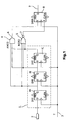
- Figure 1 shows an embodiment of the invention in which a register chain 1 comprises three registers 1A, 1B and 1C connected in succession. Connected to an input D1A of a first register 1A is an input line 2 which is used to transmit a serial data stream. A noninverting output Q1A of the first register 1A is connected to an input D1B of a second register 1B; the output Q2B of the latter is connected to an input D1C of a third register 1C in the register chain 1. Each register in the register chain 1 is connected to a clock line 3, which is used to transmit a sampling clock signal T.
- the noninverting outputs Q1A, Q1B, Q1C of the registers 1A, 1B, 1C are each connected to inputs of an AND gate 4 and of a NOR gate 5.
- An output 6 of the AND gate 4 and an output 7 of the NOR gate 5 are each connected to a further register 8, to which an output line 9 is connected.
- the AND gate 4, the NOR gate 5 and the further register 8 together form a switching device for switching a logic level on the output line 9.
- the output 6 of the AND gate 4 switches to a "1" level only when the outputs Q1A, Q1B, Q1C of all three registers 1A, 1B, 1C have a logic "1" level.
- the output 7 of the NOR gate 5 switches to a logic "1" level only when all the outputs Q1A, Q1B, Q1C of the registers 1A, 1B, 1C are at the logic "0" level.
- the output 6 of the AND gate 4 is connected to an S-input of the further register 8, which is in the form of an SR-type flip-flop.
- the output 7 of the NOR gate 5 is connected to an R-input of the SR-type flip-flop.
- the further register 8, which is in the form of an SR-type flip-flop, is clocked by means of the sampling clock signal T, in the same way as the three registers 1A, 1B, 1C in the register chain 1.
- the output signal from the input filter stage is switched to logic "1" upon the next clock signal edge. If the R-input of the SR-type flip-flop 8 assumes a logic "1” level, the output signal is reset to "0" upon the next clock signal edge. If the S-input and the R-input both have a logic "0", the output signal maintains the previous value (value stored for the preceding clock signal edge of the sampling clock signal T).
- a logic "1” is generally applied to the input if the signal profile is not subject to interference. After three rising edges of the sampling clock signal T, this logic “1” has been transferred into the three registers 1A, 1B, 1C in the register chain 1.
- the outputs Q1A, Q1B, Q1C thereof each have a logic "1" level.
- the frequency of the sampling clock signal T is preferably a multiple of the frequency of the input signal (of the serial data), with the result that no significant delays arise between an input signal change and the change in the output signal.
- any signal pulse which is smaller than the threefold clock period of the sampling clock signal T is not passed on to the output. Since the frequency of the input signals is very much lower than that of the sampling clock signal T, such short pulses are usually just interference pulses or voltage spikes, which are unwanted and must not be passed on to the output of the input filter stage.
- the register chain 1, having three registers 1A, 1B, 1C connected in succession, which is used in the embodiment described above serves to illustrate the principle of the invention.
- the register chain 1 can also comprise more than three registers.
- the register chain 1 and the frequency of the sampling clock signal T need to be tuned such that the register chain 1 is long enough to filter the longest reflections or interference out of the input signal without suppressing valid data signals in the process.
- the maximum duration of an interference signal filtered out by an input filter is obtained from multiplying the number of registers in the register chain 1 by the clock period of the sampling clock signal T.
- An input filter can thus be configured for any desired area. This is done when designing the input filter, first by choosing a suitable number of registers for the register chain 1. Secondly, the frequency of the sampling clock signal T is selected. For this, it should be noted that the larger the interference pulses which are able to be suppressed by this input filter, the greater the delay also in the input filter between the input signal and the output signal.
- the registers in the register chain 1 are in the form of D-type flip-flops. However, it is also possible to use other register types or switching elements suitable for constructing a shift register.
- the AND gate 4, the NOR gate 5 and the SR-type flip-flop 8 together form one possible switching apparatus for switching the output line 9 to the logic level of the registers 1A, 1B, 1C in the register chain 1 when the outputs Q1A, Q1B, Q1C of all three registers 1A, 1B, 1C have assumed either a "1" level or a "0" level.
- Such a switching apparatus can naturally also be produced using other switching elements if the logic function on which the invention is based is retained.
- the essential feature here is that the output signal level of the input filter changes only when a change in the input signal affects all the outputs Q1A, Q1B, Q1C of the registers 1A, 1B, 1C in the register chain 1.
- the input filter stage described can be used in an I2C bus system, for example. Since, in the I2C bus, serial data is usually transmitted via unscreened lines, the transmission rates are limited. By way of example, the maximum frequency of the input signals in the embodiment described above is 400 kHz and the sampling clock rate is 50 MHz. Any interference pulse of less than 3x20 ns is filtered out by this input filter stage.
- This input filter stage can naturally be used to filter serial data streams irrespective of the particular transmission protocol and irrespective of the data frequency.
- the digital circuit shown schematically in Figure 1 can be produced with little outlay and can preferably be formed, together with logic connected downstream or an evaluation circuit, on an integrated circuit.
- the additional hardware involvement as a result of the input filter is negligibly low by comparison with today's chip sizes.
- I2C bus This is a bus which is used to transmit the data words serially.
- the invention may also be used in bus systems in which the data words are transmitted in parallel, however. In this case, the register chain mentioned needs to be provided for each individual data line.
Landscapes
- Engineering & Computer Science (AREA)
- Physics & Mathematics (AREA)
- Nonlinear Science (AREA)
- Power Engineering (AREA)
- Computer Networks & Wireless Communication (AREA)
- Signal Processing (AREA)
- Manipulation Of Pulses (AREA)
- Picture Signal Circuits (AREA)
- Dc Digital Transmission (AREA)
Abstract
Description
The essential advantage obtained by the invention over the prior art is that little circuit complexity is used to provide a possibility for suppressing interference on bus lines in data streams, particularly for suppressing interference which occurs as a result of line reflections or crosstalk.
Claims (13)
- Input filter stage for filtering a data stream supplied via an input line, characterized by a register chain (1), which is connected to the input line (2) and has a plurality of series-connected registers (1A, 1B, 1C), and a switching device (4, 5, 8) connected to an output line (9) and to the register chain (1) in order to switch the output line (9), a signal input of a first register (1A) in the register chain (1) being connected to the input line (2), and a signal input of a subsequent register (1B or 1C) in the register chain (1) being connected to a respective signal output of a preceding register (1A or 1B) in the register chain (1), a clock input for the plurality of registers (1A, 1B, 1C) being connected to a respective clock line (3) which can be used to transmit a sampling signal (T) at a sampling frequency, the sampling frequency being higher than a maximum data transmission frequency of the data stream, and the switching device (4, 5, 8) being connected to the register chain (1) such that the output line (9) can be switched to a logic level of the signal outputs of the plurality of registers (1A, 1B, 1C) when output signals which are produced at each of the signal outputs of the plurality of registers (1A, 1B, 1C) are at the same logic level.
- Input filter stage according to Claim 1, characterized in that the plurality of registers (1A, 1B, 1C) are each in the form of D-type flip-flops.
- Input filter stage according to one of the preceding claims, characterized in that the register chain (1) comprises three registers (1A, 1B, 1C).
- Input filter stage according to one of the preceding claims, characterized in that the sampling frequency is a plurality of times higher than the maximum data transmission frequency of the data stream.
- Input filter stage according to one of the preceding claims, characterized in that the sampling frequency is approximately 50 MHz.
- Input filter stage according to one of the preceding claims, characterized in that the circuit device comprises an AND gate (4), a NOR gate (5) and a further register (8), inputs of the AND gate (4) and of the NOR gate (5) each being connected to the signal output of one of the plurality of registers (1A, 1B, 1C), and outputs of the AND gate (4) and of the NOR gate (5) each being connected to inputs of the further register (8).
- Input filter stage according to Claim 6, characterized in that the further register (8) is in the form of an SR-type flip-flop.
- I2C bus interface, characterized by an input filter stage according to one of Claims 1 to 7.
- Integrated circuit, characterized by an input filter stage according to one of Claims 1 to 7.
- Method for filtering a data stream in a filter input stage which comprises a serial register chain (1), connected to an input line (2), and a switching device (4, 5, 8), connected to the serial register chain (1) and to an output line (9), the method having the following method steps:the data is serially transferred using the serial register chain (1), registers (1A, 1B, 1C) in the serial register chain (1) each being clocked at a sampling frequency which is higher than a maximum data transmission frequency of the data stream; andthe switching device (4, 5, 8) is used to switch the output line (9) to a logic output level when signal outputs of the registers (1A, 1B, 1C) in the serial register chain (1) are at the same logic level.
- Method according to Claim 10, where the circuit device (4, 5, 8) comprises an SR-type flip-flop (8), characterized in that the output line (9) is switched by means of the SR-type flip-flop (8), an S-input of the SR-type flip-flop (8) assuming a logic "1" level only when the same logic level of the signal outputs of the registers (1A, 1B, 1C) is a logic "1" level, and an R-input of the SR-type flip-flop (8) assuming a logic "1" level only when the same logic level of the signal outputs of the registers (1A, 1B, 1C) is a logic "0" level.
- Method according to Claim 10 or 11, characterized in that the sampling frequency is a plurality of times higher than the maximum data transmission frequency of the data stream on the input line.
- Method according to one of Claims 10 to 12, characterized in that the sampling frequency is approximately 50 MHz.
Applications Claiming Priority (2)
| Application Number | Priority Date | Filing Date | Title |
|---|---|---|---|
| DE19960785 | 1999-12-16 | ||
| DE19960785A DE19960785A1 (en) | 1999-12-16 | 1999-12-16 | Input filter stage for a data stream and method for filtering a data stream |
Publications (2)
| Publication Number | Publication Date |
|---|---|
| EP1109315A2 true EP1109315A2 (en) | 2001-06-20 |
| EP1109315A3 EP1109315A3 (en) | 2003-08-13 |
Family
ID=7932952
Family Applications (1)
| Application Number | Title | Priority Date | Filing Date |
|---|---|---|---|
| EP00126362A Withdrawn EP1109315A3 (en) | 1999-12-16 | 2000-12-02 | Input filter stage for a data stream, and method for filtering a data stream |
Country Status (5)
| Country | Link |
|---|---|
| US (1) | US6414540B2 (en) |
| EP (1) | EP1109315A3 (en) |
| JP (1) | JP2001211057A (en) |
| CN (1) | CN1176522C (en) |
| DE (1) | DE19960785A1 (en) |
Cited By (4)
| Publication number | Priority date | Publication date | Assignee | Title |
|---|---|---|---|---|
| US7999596B2 (en) | 2009-03-26 | 2011-08-16 | Texas Instruments Incorporated | Digital suppression of spikes on an 12C bus |
| WO2015167954A1 (en) * | 2014-04-28 | 2015-11-05 | Qualcomm Incorporated | Sensors global bus |
| US10417172B2 (en) | 2014-04-28 | 2019-09-17 | Qualcomm Incorporated | Sensors global bus |
| CN111801656A (en) * | 2018-10-29 | 2020-10-20 | 深圳配天智能技术研究院有限公司 | Robot control system, heartbeat monitoring method and monitoring module, storage medium |
Families Citing this family (11)
| Publication number | Priority date | Publication date | Assignee | Title |
|---|---|---|---|---|
| US6914951B2 (en) * | 2001-07-24 | 2005-07-05 | Hewlett-Packard Development Company, L.P. | Method and apparatus for a digital logic input signal noise filter |
| JP2006332945A (en) * | 2005-05-25 | 2006-12-07 | Nec Electronics Corp | Semiconductor integrated circuit |
| GB2437121A (en) * | 2006-04-11 | 2007-10-17 | Wolfson Microelectronics Plc | A debounce circuit with low latency |
| US8149038B1 (en) * | 2010-03-22 | 2012-04-03 | Altera Corporation | Techniques for phase adjustment |
| DE112014003074B4 (en) | 2014-06-02 | 2021-01-14 | Mitsubishi Electric Corporation | Noise analyzer, electronic device and noise source identification system |
| US20170052774A1 (en) * | 2015-08-18 | 2017-02-23 | Google Inc. | User acquisition via bidding for connected device app installs |
| CN105356865B (en) * | 2015-12-09 | 2018-09-21 | 深圳Tcl数字技术有限公司 | Remove the method, apparatus and smart television of interference |
| CN110912539B (en) * | 2018-09-14 | 2025-02-21 | 恩智浦美国有限公司 | Clock generator and method for generating clock signal |
| US20220103165A1 (en) * | 2018-12-27 | 2022-03-31 | Ams International Ag | Filters for removing disturbances from signals |
| CN111277242B (en) * | 2020-03-26 | 2025-03-14 | 广州鸿威技术有限公司 | A FPGA digital filter and its implementation method |
| CN112234965A (en) * | 2020-09-18 | 2021-01-15 | 浙江吉利控股集团有限公司 | A switch debounce circuit and electronic equipment |
Family Cites Families (16)
| Publication number | Priority date | Publication date | Assignee | Title |
|---|---|---|---|---|
| US4525635A (en) * | 1982-12-15 | 1985-06-25 | Rca Corporation | Transient signal suppression circuit |
| US4585997A (en) * | 1983-12-08 | 1986-04-29 | Televideo Systems, Inc. | Method and apparatus for blanking noise present in an alternating electrical signal |
| JPS6282713A (en) * | 1985-10-07 | 1987-04-16 | Hitachi Ltd | Waveform shaping circuit and magnetic recording/playback device using the same |
| DE3913395A1 (en) * | 1989-04-24 | 1990-10-25 | Grundig Emv | DIGITAL FILTER LOGIC |
| JPH02283120A (en) * | 1989-04-25 | 1990-11-20 | Toshiba Corp | Noise eliminator |
| US5001374A (en) * | 1989-09-08 | 1991-03-19 | Amp Incorporated | Digital filter for removing short duration noise |
| JPH0449409A (en) * | 1990-06-19 | 1992-02-18 | Melco:Kk | Noise preventing circuit for parallel interface |
| JPH0475121A (en) * | 1990-07-17 | 1992-03-10 | Mitsubishi Electric Corp | Input interface circuit for automobile |
| JP2692415B2 (en) * | 1991-05-15 | 1997-12-17 | 日本電気株式会社 | Pulse removal circuit |
| DE4220557C2 (en) | 1992-06-24 | 1999-01-07 | Kommunikations Elektronik | Digital message transmission method |
| US5386159A (en) * | 1993-06-30 | 1995-01-31 | Harris Corporation | Glitch suppressor circuit and method |
| US5563532A (en) | 1994-01-24 | 1996-10-08 | Advanced Micro Devices, Inc. | Double filtering glitch eater for elimination of noise from signals on a SCSI bus |
| US5418486A (en) * | 1994-01-28 | 1995-05-23 | Vlsi Technology, Inc. | Universal digital filter for noisy lines |
| US5553070A (en) * | 1994-09-13 | 1996-09-03 | Riley; Robert E. | Data link module for time division multiplexing control systems |
| US5663675A (en) * | 1995-06-07 | 1997-09-02 | American Microsystems, Inc. | Multiple stage tracking filter using a self-calibrating RC oscillator circuit |
| KR100247419B1 (en) * | 1997-05-27 | 2000-04-01 | 강병호 | Redundant Active / Standby Control Using Gap Removal Circuit |
-
1999
- 1999-12-16 DE DE19960785A patent/DE19960785A1/en not_active Withdrawn
-
2000
- 2000-12-02 EP EP00126362A patent/EP1109315A3/en not_active Withdrawn
- 2000-12-13 CN CNB001321013A patent/CN1176522C/en not_active Expired - Fee Related
- 2000-12-14 JP JP2000380212A patent/JP2001211057A/en active Pending
- 2000-12-14 US US09/737,077 patent/US6414540B2/en not_active Expired - Fee Related
Cited By (11)
| Publication number | Priority date | Publication date | Assignee | Title |
|---|---|---|---|---|
| US7999596B2 (en) | 2009-03-26 | 2011-08-16 | Texas Instruments Incorporated | Digital suppression of spikes on an 12C bus |
| US8248134B2 (en) | 2009-03-26 | 2012-08-21 | Texas Instruments Incorporated | Digital suppression of spikes on an I2C bus |
| WO2015167954A1 (en) * | 2014-04-28 | 2015-11-05 | Qualcomm Incorporated | Sensors global bus |
| US9734121B2 (en) | 2014-04-28 | 2017-08-15 | Qualcomm Incorporated | Sensors global bus |
| US9921998B2 (en) | 2014-04-28 | 2018-03-20 | Qualcomm Incorporated | Sensors global bus |
| EP3392779A1 (en) * | 2014-04-28 | 2018-10-24 | Qualcomm Incorporated | Sensors global bus |
| US10417172B2 (en) | 2014-04-28 | 2019-09-17 | Qualcomm Incorporated | Sensors global bus |
| US10452603B2 (en) | 2014-04-28 | 2019-10-22 | Qualcomm Incorporated | Sensors global bus |
| US10482057B2 (en) | 2014-04-28 | 2019-11-19 | Qualcomm Incorporated | Multi-protocol dynamic address allocation |
| CN111801656A (en) * | 2018-10-29 | 2020-10-20 | 深圳配天智能技术研究院有限公司 | Robot control system, heartbeat monitoring method and monitoring module, storage medium |
| CN111801656B (en) * | 2018-10-29 | 2023-12-22 | 深圳配天机器人技术有限公司 | Robot control system, heartbeat monitoring method and monitoring module, storage medium |
Also Published As
| Publication number | Publication date |
|---|---|
| US6414540B2 (en) | 2002-07-02 |
| EP1109315A3 (en) | 2003-08-13 |
| CN1176522C (en) | 2004-11-17 |
| US20010004731A1 (en) | 2001-06-21 |
| JP2001211057A (en) | 2001-08-03 |
| CN1305265A (en) | 2001-07-25 |
| DE19960785A1 (en) | 2001-06-21 |
Similar Documents
| Publication | Publication Date | Title |
|---|---|---|
| US6414540B2 (en) | Input filter stage for a data stream, and method for filtering a data stream | |
| US5001374A (en) | Digital filter for removing short duration noise | |
| US6175603B1 (en) | System for managing signals in different clock domains and a programmable digital filter | |
| US8558579B2 (en) | Digital glitch filter | |
| US5555213A (en) | Interface circuit, system and method for interfacing an electronic device and a synchronous state machine having different clock speeds | |
| WO1996041417A1 (en) | Glitch-free clock enable circuit | |
| US5760612A (en) | Inertial delay circuit for eliminating glitches on a signal line | |
| US5159278A (en) | State machine architecture providing increased resolution of output timing | |
| US7557643B2 (en) | De-glitch circuit | |
| KR20080101495A (en) | Clock switching circuit | |
| JPH0758609A (en) | Glitch suppression circuit and method thereof | |
| US4949360A (en) | Synchronizing circuit | |
| EP0723719B1 (en) | Circuit arrangement for converting a serial data signal into a parallel data signal | |
| US6937953B2 (en) | Circuit configuration for receiving at least two digital signals | |
| US7197053B1 (en) | Serializer with programmable delay elements | |
| US6262602B1 (en) | Incident-edge detecting probe | |
| US6081905A (en) | Method and apparatus for generating a clock signal from a plurality of clock phases | |
| US20080174338A1 (en) | Filter circuit for removing noise pulses from digital input signal | |
| KR940009333B1 (en) | Integrated electronic multiplex circuit | |
| JP2003163583A (en) | Asynchronous noise filter circuit | |
| US20070069793A1 (en) | Method and system for high frequency clock signal gating | |
| KR0152346B1 (en) | Clock switching circuit | |
| JPH05336091A (en) | Bus communication system | |
| SU1389008A2 (en) | Device for receiving bipulsed signal | |
| US6741657B1 (en) | Circuit arrangement for transmitting pulses via a transmission path |
Legal Events
| Date | Code | Title | Description |
|---|---|---|---|
| PUAI | Public reference made under article 153(3) epc to a published international application that has entered the european phase |
Free format text: ORIGINAL CODE: 0009012 |
|
| AK | Designated contracting states |
Kind code of ref document: A2 Designated state(s): AT BE CH CY DE DK ES FI FR GB GR IE IT LI LU MC NL PT SE TR |
|
| AX | Request for extension of the european patent |
Free format text: AL;LT;LV;MK;RO;SI |
|
| PUAL | Search report despatched |
Free format text: ORIGINAL CODE: 0009013 |
|
| AK | Designated contracting states |
Designated state(s): AT BE CH CY DE DK ES FI FR GB GR IE IT LI LU MC NL PT SE TR |
|
| AX | Request for extension of the european patent |
Extension state: AL LT LV MK RO SI |
|
| AKX | Designation fees paid | ||
| REG | Reference to a national code |
Ref country code: DE Ref legal event code: 8566 |
|
| STAA | Information on the status of an ep patent application or granted ep patent |
Free format text: STATUS: THE APPLICATION IS DEEMED TO BE WITHDRAWN |
|
| 18D | Application deemed to be withdrawn |
Effective date: 20040214 |