BACKGROUND OF THE INVENTION
1. Field of the Invention
The present invention generally relates to
processors and methods of controlling processors,
and, more particularly, to a processor that executes
programmed instructions and a method of controlling
such a processor.
2. Description of the Related Art
FIG. 1 shows a first example of a
conventional processor having a general register and
a floating point register. As shown in FIG. 1, the
processor comprises a memory 1, an instruction read
unit 3 connected to the memory 1, an instruction
execution unit 5 connected to the memory 1 and the
instruction read unit 3, a register control unit 7
connected to the instruction execution unit 5, and
an interrupt control unit 9 connected to the
instruction read unit 3, the instruction execution
unit 5, and the register control unit 7.
The instruction read unit 3 includes an
instruction read control unit 11, a program counter
(PC) 13, and an instruction word register (IR) 15.
The instruction read control unit 11 is connected to
the memory 1, and the program counter (PC) 13 is
connected to the instruction read control unit 11.
The instruction word register (IR) 15 is connected
to the instruction read control unit 11.
The instruction execution unit 5 includes
an instruction decoder unit 17, a load instruction
execution unit 19, a store instruction execution
unit 21, an instruction execution circuit 23, a
gloating point load instruction execution unit 25, a
floating point store instruction execution unit 27,
and a floating point calculation instruction
execution unit 29.
The instruction decoder unit 17 is
connected to the instruction word register 15, and
the load instruction execution unit 19 is connected
to the memory 1 and the instruction decoder unit 17.
The store instruction execution unit 21 is
connected to the instruction decoder unit 17 and a
general register 37 that will be described later.
The instruction execution circuit 23 is connected to
the instruction decoder unit 17, the general
register 37, and registers 31, 33, and 35 that will
be described later. The floating point load
instruction execution unit 25 is connected to the
memory 1 and the instruction decoder unit 17. The
floating point store instruction execution unit 27
and the floating point calculation instruction
execution unit 29 are connected to the instruction
decoder unit 17 and a floating point register 39
that will be described later.
Meanwhile, the register control unit 7
includes an EPCR register 31, an EPSR register 33, a
PSR register 35, the general register 37, and the
floating point register 39. The EPCR register 31,
the EPSR register 33, and the PSR register 35 are
connected to an interrupt control circuit 40. The
general register 37 is connected to the load
instruction execution unit 19, the store instruction
execution unit 21, and the instruction execution
circuit 23. The floating point register 39 is
connected to the floating point load instruction
execution unit 25, the floating point store
instruction execution unit 27, and the floating
point arithmetic operation instruction execution
unit 29.
The interrupt control unit 9 includes the
interrupt control circuit 40. The interrupt control
circuit 40 is connected to the instruction read
control unit 11, the program counter 13, the load
instruction execution unit 19, the store instruction
execution unit 21, the instruction execution circuit
23, the floating point load instruction execution
unit 25, the floating point store instruction
execution unit 27, and the floating point arithmetic
operation instruction execution unit 29.
In the processor having the above
structure, the instruction read unit 3 reads an
instruction word indicated by the program counter 13
out of the memory 1, and supplies the instruction
word to the instruction execution unit 15 via the
instruction word register (IR) 15. If the
instruction read control unit 11 receives a branch
destination address from the instruction execution
unit 5 and the interrupt control circuit 40, which
executes an interrupt, the instruction read control
unit 11 writes the branch destination address in the
program counter 13. In other cases, the instruction
read control unit 11 supplies a next instruction
word to the instruction execution unit 5, and
therefore increments the program counter 13 that
indicates the address of the instruction word to be
read out. In a case where the instruction read
control unit 11 detects an interrupt when reading an
instruction word, the instruction read control unit
11 supplies an interrupt signal to the interrupt
control circuit 40.
The instruction decoder unit 17 decodes an
instruction supplied from the instruction word
register 15. In a case of a load instruction, the
instruction decoder unit 17 supplies the instruction
to the load instruction execution unit 19. In a
case of a store instruction, the instruction decoder
unit 17 supplies a store instruction to the store
instruction execution unit 21. In a case of a
floating point load instruction, the instruction
decoder unit 17 supplies the instruction to the
floating point load instruction execution unit 25.
In a case of a floating point store instruction, the
instruction decoder unit 17 supplies the instruction
to the floating point store instruction execution
unit 27. In a case of a floating point calculating
instruction, the instruction decoder unit 17
supplies the instruction to the floating point
calculating instruction execution unit 29. In a
case of an interrupt return instruction to any other
instruction, the instruction decoder unit 17
supplies the instruction to the instruction
execution circuit 23.
When the load instruction execution unit
19 receives the load instruction, the load
instruction execution unit 19 reads data from a
region in the memory 1 corresponding to an effective
address determined based on a value read out from
the general register 37, and writes the result in
the general register 37, as shown in FIG. 2. Here,
the load instruction includes an instruction code
OP-CODE, and codes GR1, GR2, and GRD for designating
a register. The addition result of the register
value indicated by the code GR1 and the register
value indicated by the code GR2 represents the
address of the data to be loaded, and the code GRD
indicates the number of a register that holds the
addition result. However, in a case where the load
instruction execution unit 19 detects an interrupt
when executing the load instruction, the load
instruction execution unit supplies an interrupt
signal to the interrupt control circuit 40.
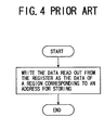
Likewise, when the store instruction
execution unit 21 receives the store instruction,
the store instruction execution unit 21 reads data
from the region in the general register 37
corresponding to an effective address determined
based on a value read out from the general register,
and writes the result in the region of the memory 1
corresponding to the effective address, as shown in
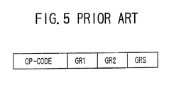
FIG. 4. Here, the store instruction includes an
instruction code OP-CODE, and codes GR1, GR2, and
GRS for designating a register. The addition result
of the register value indicated by the code GR1 and
the register value indicated by the code GR2
represents the address of data to be stored, and the
code GRS indicates the number of a register that
holds a value to be written. However, in a case the
store instruction execution unit 21 detects an
interrupt when executing the store instruction, the
store instruction execution unit 21 supplies an
interrupt signal to the interrupt control circuit 40.
When the floating point load instruction
execution unit 25 receives the floating point load
instruction, the floating point load instruction
execution unit 25 reads data from the region in the
memory 1 corresponding to an effective address
determined based on a value read out from the
general register 37, and writes the result in the
floating point register 39. However, in a case
where the floating point load instruction execution
unit 25 detects an interrupt when executing the
floating point load instruction, the floating point
load instruction execution unit 25 supplies an
interrupt signal to the interrupt control circuit 40.
When the floating point store instruction
execution unit 27 receives the floating point store
instruction, the floating point store instruction
execution unit 27 reads data from the region in the
floating point register 39 corresponding to an
effective address determined based on a value read
out from the general register 37, and writes the
result in the region memory 1 corresponding to the
effective address. However, in a case where the
floating point store instruction execution unit 27
detects an interrupt while executing the floating
point store instruction, the floating point store
instruction execution unit 27 supplies an interrupt
signal to the interrupt control circuit 40.
The floating point arithmetic operation
instruction execution unit 29 executes an operation
based on a value read out from the floating point
register 39 when the floating point arithmetic
operation instruction is supplied. The floating
point arithmetic operation instruction execution
unit 29 then writes the result in the floating point
register 39.
When the instruction execution circuit 23
receives an arithmetic operation instruction from
the instruction decoder unit 17, the instruction
execution circuit 23 performs an operation based on
a value read out from the general register 37, and
writes the result in the general register 37. In a
case where the instruction execution circuit 23
receives a branch instruction from the instruction
decoder unit 17, the instruction execution circuit
23 supplies the branch destination address to the
program counter 13 at the time of the occurrence of
the branch. In a case where the instruction
execution circuit 23 receives an interrupt return
instruction, the instruction execution circuit 23
writes data that represents the pre-interrupt
operation state in the register PSR 35. The
instruction execution circuit 23 then reads the
address of the instruction at the return destination
from the register EPCR 31, and supplies the address
as the branch destination address to the program
counter 13. However, if the instruction execution
circuit 23 detects an interrupt while executing the
above instruction, the instruction execution circuit
23 supplies an interrupt signal to the interrupt
control circuit 40.
The register EPCR 31 holds the address of
an instruction corresponding to the return
destination from the interrupt. The address is set
at the occurrence of the interrupt. The register
PSR 35 holds data that represents the operation
state, and the register EPSR 33 holds data that
represents the pre-interrupt operation state set
prior to the occurrence of the interrupt.
Based on the interrupt signal supplied
from the instruction read unit 3 or the instruction
execution unit 5, the interrupt control circuit 40
writes the instruction address corresponding to the
interrupt return destination in the register EPCR 31,
the data that represents the pre-interrupt operation
state in the register EPSR 33, and the operation
state corresponding to the interrupt in the PSR 35.
The interrupt control circuit 40 supplies the branch
destination address corresponding to the interrupt
to the instruction read unit 3.
In the following, the operations of the
above processor will be summarized. The operation
of the processor in the initial stage is as follows.
The instruction read unit 3 reads out an instruction
word indicated by the program counter 13, supplies
the instruction word to the instruction execution
unit 5, and then executes the supplied instruction.
When an interrupt occurs, the interrupt
control circuit 40 writes the instruction address
corresponding to the interrupt return destination in
the register EPCR 31, the data that represents the
pre-interrupt operation state in the EPSR 33, and
the operation state of the interrupt in the PSR 35,
based on the interrupt signal supplied from the
instruction read unit 3 or the instruction execution
unit 5. Also, the interrupt control circuit 40
supplies the branch destination address
corresponding to the interrupt to the instruction
read unit 3. The instruction read unit 3 then reads
out an instruction word in accordance with the
branch destination address supplied from the
interrupt control unit 9, and supplies the
instruction word to the instruction execution unit 5.
After that, the operation is carried out in the same
manner as in the normal state described above.
At the time of interrupt return, the
instruction execution unit 5 executes an interrupt
return instruction, thereby writing the value of the
register EPSR 33 in the register PSR 35. The
instruction execution unit 5 reads out the data from
the register EPCR 31, and supplies the result as the
branch destination address to the instruction read
unit 3. The instruction read unit 3 in turn reads
out an instruction word in accordance with the
branch destination address supplied from the
instruction execution unit 5, and supplies the
instruction word to the instruction execution unit 5.
After that, the operation is performed in the same
manner as in the above-described normal state.
FIG. 6 shows a second example of the
conventional processor having a general register and
a floating point register. This processor has the
same structure as the processor of the first example,
except that an instruction execution unit 6 further
comprises an arithmetic operation instruction
execution unit 22, and a register control unit 8
further comprises a condition register 30. In FIG.
6, the same components as in FIG. 1 are denoted by
the same reference numerals, and explanations for
them are omitted in this description.
When receiving an arithmetic instruction,
the arithmetic operation instruction execution unit
22 reads out data from the region in the general
register 37 corresponding to an effective address
determined based on a value read out from the
general register 37, and performs an arithmetic
operation based on the read data. The result of the
arithmetic operation is then written in the general
register 37, as shown in FIG. 7. The arithmetic
operation instruction has the same format as the
load instruction shown in FIG. 3. When receiving a
comparison instruction, the arithmetic operation
instruction execution unit 22 compares two values
read out from the general register 37. If the two
values are equal, the arithmetic operation
instruction execution unit 22 writes the data
indicating truth in the condition register 30. If
the two values are not equal, the arithmetic
operation instruction execution unit 22 writes data
indicating false in the condition register 30.
FIG. 8 shows a third example of the
conventional processor. In FIG. 8, the same
components as in FIG. 6 are denoted by the same
reference numerals, and explanations for them are
omitted in this description. As shown in FIG. 8,
this processor comprises the memory 1, an
instruction read unit 303 connected to the memory 1,
an instruction execution unit 307 connected to the
memory 1 and the instruction read unit 303, a
register control unit 309 connected to the
instruction execution unit 307, and the interrupt
control unit 9 connected to the instruction read
unit 303, the instruction execution unit 307, and
the register control unit 309.
The instruction read unit 303 comprises
the instruction read control unit 11, the program
counter 13 the instruction word register 15, and an
instruction break detector unit 301. The
instruction break detector unit 301 is connected to
the memory 1 and the instruction execution circuit
23.
The instruction execution unit 307
comprises the instruction decoder unit 17, the load
instruction execution unit 19, the store instruction
execution unit 21, the arithmetic operation
instruction execution unit 22, the instruction
execution circuit 23, and a data break detector unit
305. The data break detector unit 305 is connected
to the load instruction execution unit 19, the store
instruction execution unit 21, and the instruction
execution circuit 23.
The interrupt control circuit 40 is
connected to the instruction read control unit 11,
the program counter 13, the instruction break
detector unit 301, the load instruction execution
unit 19, the store instruction execution unit 21,
the arithmetic operation instruction execution unit
22, the instruction execution circuit 23, and the
data break detector unit 305.
When receiving a break point instruction
from the instruction decoder unit 17, the
instruction execution circuit 23 notifies the
interrupt control circuit 40 of the software break.
When receiving an instruction break point register
read instruction from the instruction decoder unit
17, the instruction execution circuit 23 reads a
break point object address from an instruction break
point register in the instruction break detector
unit 301, and writes the read address in the general
register 37. When receiving an instruction break
point register write instruction from the
instruction decoder unit 17, the instruction
execution circuit 23 writes the break point object
address corresponding to a value read out from the
general register 37 into the instruction break point
register in the instruction break detector break
detector unit 301.
Likewise, when receiving a data break
point register read instruction from the instruction
decoder unit 17, the instruction execution circuit
23 reads out a break point object address from a
data break point register in the data break detector
unit 305, and writes the read address into the
general register 37. When receiving a data break
point register write instruction from the
instruction decoder unit 17, the instruction
execution circuit 23 writes the break point object
address corresponding to a value read out from the
general register 37 into the data break point
register in the data break detector unit 305.
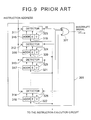
FIG. 9 shows the structure of the
instruction break detector unit 301. As shown in
FIG. 9, the instruction break detector 301 comprises
detectors 311 to 314, address fields 315 to 318, E
fields 319 to 322, V fields 323 to 326, and an OR
circuit 327.
The address fields 315 to 318 each hold a
break point object address, and constitute the
above-mentioned instruction break point register.
The E fields 319 to 322 each holds data that
indicates whether or not an instruction break
operation is valid. More specifically, when the
instruction break operation is invalid, the
corresponding one of the E fields 319 to 322 holds
the value "0". When the instruction break operation
is valid, the corresponding one of the E fields 319
to 322 holds the value "1". The E fields 319 to 322
constitute the above-mentioned instruction break
point register. The V fields 323 to 326 each hold
data that indicates whether or not an instruction
break has been detected. More specifically, if no
instruction break has been detected, the
corresponding one of the V fields 323 to 326 holds
the value "0". If an instruction break has been
detected, the corresponding one of the V fields 323
to 326 holds the value "1".
The detectors 311 to 314 each determine
whether or not an instruction break is established.
More specifically, each of the detectors 311 to 314
compares an instruction address supplied from the
memory 1 with an address supplied from the
instruction break point register. If the two
addresses coincide with each other, the value "1" is
written in the corresponding one of the V fields 323
to 326, and a match signal mt is supplied to the OR
circuit 327. An interrupt signal is then
transmitted form the OR circuit 327 to the interrupt
control circuit 40, thereby notifying the interrupt
control circuit 40 of the instruction break.
FIG. 10 shows the structure of the data
break detector unit 305. As shown in FIG. 10, the
data break detector unit 305 also comprises the
detectors 311 to 314, the address fields 315 to 318,
the E fields 319 to 322, the V fields 323 to 326,
and the OR circuit 327.
The address fields 315 to 318 each hold a
break point object address, and constitute the
above-mentioned data break point register. The E
fields 319 to 322 each hold data that indicates
whether or not a data break operation is valid.
More specifically, if the data break operation is
invalid, the corresponding one of the E fields 319
to 322 holds the value "1". If the data break
operation is valid, the corresponding one of the E
fields 319 to 322 holds the value "0". The E fields
319 to 322 constitute the data break point register.
The V fields 323 to 326 each hold data that
indicates whether or not a data break has been
detected. More specifically, when no data break has
been detected, the corresponding one of the V fields
323 to 326 holds the value "0". When a data break
has been detected, the corresponding one of the V
fields 323 to 326 holds the value "1".
The detectors 311 to 314 each determine
whether or not a data break is established. More
specifically, the detectors 311 to 314 each compare
an effective address (data address of a load store
instruction supplied form the memory 1 with a break
point object address stored in the corresponding one
of the address fields 315 to 318. When the two
addresses coincides with each other, "1" is written
in the corresponding one of the V fields 323 to 326,
and a match signal mt is supplied to the OR circuit
327. By doing so, an interrupt signal is supplied
from the OR circuit 327 to the interrupt control
circuit 40, thereby notifying the interrupt control
circuit 40 of the data break.
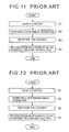
FIG. 11 is a flowchart showing a data
break interrupt operation of the above processor by
an interrupt operation program. As shown in FIG. 11,
a context is saved in step S1, and a data break
operation is performed in step S2. The context is
then restored in step S3, and an interrupt return
instruction is executed so as to return from the
interrupt operation in step S4. The interrupt
operation then comes to an end.
FIG. 12 is a flowchart showing a software
break interrupt operation by the interrupt operation
program. As shown in FIG. 12, a context is saved in
step S1, and a software break operation is performed
in step S2. The context is restored in step S3, and
an interrupt return instruction is executed so as to
return from the interrupt operation in step S4. The
interrupt operation then comes to an end.
In the above conventional processors, a
control method of simultaneously executing a
plurality of instructions, such as a superscalar
technique or a speculative execution technique, is
employed to improve the performance of the processor,
utilizing the parallelism of instruction words that
constitute a program. Generally, such a processor
comprises a plurality of instruction execution units,
and sequentially executes the instructions contained
in the program. A plurality of instructions can be
read out from the memory in one cycle, and a
plurality of instructions can be issued in one cycle,
with the dependency among the instructions being
taken into account.
In the instruction execution control, an
out-of-order completion technique is employed to
increase the performance at the instruction level of
the processor. Here, the "out-of-order completion"
indicates that the issuance order of instructions on
the program differs from the instruction execution
order, i.e., the instruction completion order. By
performing such an execution control operation, the
effective availability of the instruction execution
unit is increased, and the entire execution time of
the program is shortened. To ensure the instruction
order at the time of the generation of the program,
the data dependency relationship or the control
dependency relationship needs to be taken into
consideration. The information on the dependency
relationship is extracted from the information
written in the instruction words.
In a load operation performed on the
memory 1, data is read out from the memory 1, and
the result is written in the register in the
processor. After that, a series of operations
depending on the read data are started. Accordingly,
a load operation from the memory 1 is started so as
to reduce adverse influence onto the operation of
the entire processor from a delay of access to the
memory 1 caused by cache miss or the like.
From the above reasons, when a program is
generated, a load instruction may be placed in a
further front position in the program so as to start
the load operation in an earlier stage. In this
arrangement, the same effects as obtained by moving
the load instruction on the program can be obtained.
If the load operation is executed prior to the store
operation in the memory 1, data processing is
performed in the same execution sequence as long as
the address regions of the data in both operations
do not overlap with each other. However, even if
the address regions only partially overlap with each
other, there will be a difference in the data
process results.
More specifically, when the load operation
is performed prior to the store operation, the
previous data stored prior to the store operation is
read out by the load operation, through the store
data stored in the memory 1 by the store operation
should be read out by the load operation. With the
change in the execution sequence, the data
processing operation changes accordingly. This
problem is known as the problem of ambiguous memory
reference. In the prior art, to avoid this problem,
a load operation cannot be performed on the memory 1
prior to a store operation on the memory 1.
Meanwhile, a technique of moving
instructions beyond the boundaries between basic
blocks by a compiler is known as the wide area
instruction movement technique. Further,
instruction movement beyond condition branching in
the wide area instruction movement is known as the
speculative instruction movement technique. However,
when an exception occurs with a speculatively moved
instruction, the ability to perform an exception
operation drastically deteriorates, or an unexpected
break occurs in the program execution despite the
originally programmed sequence.
For instance, when an instruction that has
a possibility of causing a page fault with necessary
data missing from the memory is speculatively moved,
an exception operation program that causes a page
fault at the movement destination is executed,
resulting in a drop in the operation ability. If a
division instruction is speculatively moved, a zero
division operation might be carried out at the
movement destination, but the execution of the
program is stopped in such a case. An exception
caused by the execution of a speculatively moved
instruction is called a "speculative exception".
As a means to solve the above problems, a
method of delaying the occurrence of a speculative
exception using a non-exception instruction is known.
A non-exception method in which a speculative
exception operation is delayed is mentioned in the
reference "A VLIW Architecture for a Trace
Scheduling Compiler, Proceedings of the 2nd
International Conference on Architectural Support
for Programming Languages and Operating Systems, pp.
180-192, 1987 (B.P. Colwel, B.P. Nix, J.J. O'Donnel,
D.B. Papworth, and P.K. Rodman)". Meanwhile, a
method of scheduling the restart of execution from a
speculative exception is mentioned in the reference
"Sentinel Scheduling for VLIW and Superscalar
Processor, Proceedings of the Fifth International
Conference on Architectural Support for Programming
Languages and Operating Systems, pp. 238-247, 1992
(S.A. Mahlke, W.Y. Chen, W.W. Hwu, B. R. Rau, and
M.S. Schlansker)".
There are two types of exceptions: one is
an exception with which the main operation can be
continued by canceling the exception factor, like a
page fault; and the other one is an exception with
which the main operation cannot be continued, like a
zero division operation. In the data processing
operation using the non-exception instruction, each
exception is detected as a speculative exception,
and executed after a predetermined period of time.
However, since an exception operation that
can be continued and the following main operation
are performed by executing an interrupt operation
program, the program becomes too long as a whole.
As a result, the capacity required for the processor
becomes too large, and the operation speed drops
accordingly.
Furthermore, when a program including the
non-exception instruction is being debugged, there
is another problem that the execution of the program
is interrupted by a data break with an instruction
not ensured in the original execution sequence among
speculatively moved instructions.
SUMMARY OF THE INVENTION
A general object of the present invention
is to provide processors and methods of controlling
the processor in which the above disadvantages are
eliminated.
A more specific object of the present
invention is to provide a processor that performs a
load operation prior to a store operation while
avoiding ambiguous memory reference, and thus
provides ambiguous memory reference. Thus, a high-speed
operation can be realized.
Another specific object of the present
invention is to provide a processor that has higher
data processing ability and higher operation
reliability.
The above objects of the present invention
are achieved by a method of controlling a processor
that changes an execution sequence of instructions
contained in a program, the method comprising the
steps of: executing a second instruction that is
placed after a first instruction in the program,
prior to execution of the first instruction; and,
when an address of first data to be executed by the
first instruction is included in an address region
of second data to be processed by the second
instruction, overwriting an execution result of the
first instruction on data corresponding to the
address of the first data.
According to this method, disorder in data
processing due to a change to the execution sequence
of the instructions can be corrected.
The above objects of the present invention
are also achieved by a processor that executes
instructions arranged in a program, the processor
comprising:
The above objects of the present invention
are also achieved by a method of controlling a
processor that controls execution of programmed
instructions arranged in a program, the method
comprising the steps of:
According to this method, when the
exception operation is finished, the main operation
returns to the program and sequentially executes the
instructions starting from the instruction next to
the instruction that has required the exception
operation. Thus, a high-speed operation can be
realized.
The above objects of the present invention
are also achieved by a method of controlling a
processor that controls execution of instructions
arranged in a program,
the method comprising the steps of:
According to this method, when the
exception operation is finished, the main operation
returns to the program and sequentially executes the
instructions, starting from the exception start
instruction. Thus, the operation speed can be
further increased.
The above objects of the present invention
are also achieved by a processor that executes
instructions arranged in a program, the processor
comprising:
The above objects of the present invention
are also achieved by a processor that executes
instructions in a program, the processor comprising:
The above objects of the present invention
are also achieved by a method of controlling
execution of instructions in a program, the method
comprising the steps of:
According to this method, the unnecessary
break due to the advance execution of the
instruction placed after the branch instruction is
avoided. Thus, the instructions can be surely
executed in the programmed execution order.
The above objects of the present invention
are also achieved by a processor that executes
instructions in a program, the processor comprising:
The above and other objects and features
of the present invention will become more apparent
from the following description taken in conjunction
with the accompanying drawings.
BRIEF DESCRIPTION OF THE DRAWINGS
FIG. 1 shows a first example a
conventional processor having a general register and
a floating point register;
FIG. 2 is a flowchart showing an operation
in accordance with a load instruction;
FIG. 3 shows the format of the load
instruction;
FIG. 4 is a flowchart showing an operation
in accordance with a store instruction;
FIG. 5 shows the format of the store
instruction;
FIG. 6 shows a second example of the
conventional processor having a general register and
a floating point register;
FIG. 7 is a flowchart showing an operation
in accordance with an arithmetic operation
instruction;
FIG. 8 shows a third example of the
conventional processor;
FIG. 9 shows the structure of an
instruction break detector unit shown in FIG. 8;
FIG. 10 shows the structure of a data
break detector unit shown in FIG. 8;
FIG. 11 is a flowchart showing a data
break interrupt operation by an interrupt operation
program;
FIG. 12 is a flowchart showing a software
break interrupt operation by an interrupt operation
program;
FIG. 13 shows the structure of a processor
in accordance with a first embodiment of the present
invention;
FIG. 14 shows the structure of a history
control unit shown in FIG. 13;
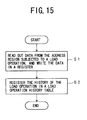
FIG. 15 is a flowchart showing an
operation in accordance with a speculative load
instruction;
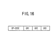
FIG. 16 shows the format of the
speculative load instruction;
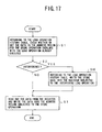
FIG. 17 is a flowchart showing an
operation in accordance with an interference
recovery store instruction;
FIG. 18 shows the format of the
interference recovery store instruction;
FIG. 19 is a flowchart showing an
operation in accordance with a speculative load
operation history nullifying instruction;
FIG. 20 shows the format of the
speculative load operation history nullifying
instruction;
FIG. 21 shows the structure of a processor
in accordance with a second embodiment of the
present invention;
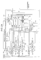
FIG. 22 shows the structure of a history
control unit shown in FIG. 21;
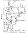
FIG. 23 shows the structure of a processor
in accordance with a third embodiment of the present
invention;
FIG. 24 shows the structure of a history
control unit shown in FIG. 23;
FIG. 25 shows the structure of a processor
in accordance with a fourth embodiment of the
present invention;
FIG. 26 shows the structure of a history
control unit shown in FIG. 25;
FIG. 27 is a flowchart showing an
operation in accordance with an interference
recovery exception store instruction;
FIG. 28 shows the format of the
interference recovery exception store instruction;
FIG. 29 is a flowchart showing an
interference recovery exception interrupt processing
program;
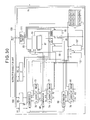
FIG. 30 shows the structure of a history
control unit in a processor in accordance with a
fifth embodiment of the present invention;
FIG. 31 shows the structure of a processor
in accordance with a sixth embodiment of the present
invention;
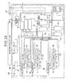
FIG. 32 shows the structure of a history
control unit shown in FIG. 31;
FIG. 33 is a flowchart showing an
operation in accordance with the interference
recovery branching store instruction;
FIG. 34 shows the format of the
interference recovery branching store instruction;
FIG. 35 shows the structure of a processor
in accordance with a seventh embodiment of the
present invention;
FIG. 36 shows the structure of a history
control unit shown in FIG. 35;
FIG. 37 is a flowchart showing an
operation in accordance with an exception inhibiting
load instruction;
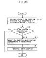
FIG. 38 is a flowchart showing an
operation in accordance with a commit instruction;
FIG. 39 shows the format of the commit
instruction;
FIG. 40 is a flowchart showing an
interrupt operation in a commit exception;
FIG. 41 shows the structure of a processor
in accordance with an eighth embodiment of the
present invention;
FIG. 42 shows the structure of a history
control unit shown in FIG. 41;
FIG. 43 is a flowchart showing an
operation in accordance with an exception inhibiting
floating point arithmetic operation instruction;
FIG. 44 shows the structure of a processor
in accordance with a ninth embodiment of the present
invention;
FIG. 45 shows the structure of a history
control unit shown in FIG. 44;
FIG. 46 is a flowchart showing an
operation in accordance with an exception inhibiting
flag nullifying instruction;
FIG. 47 shows the structure of a processor
in accordance with a tenth embodiment of the present
invention;
FIG. 48 shows the structure of a history
control unit of a processor in accordance with an
eleventh embodiment of the present invention;
FIG. 49 is a flowchart showing an
interrupt operation in a commit exception;
FIG. 50 shows the structure of a processor
in accordance with a twelfth embodiment of the
present invention;
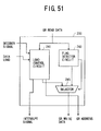
FIG. 51 shows the structure of a load
instruction execution unit shown in FIG. 50;
FIG. 52 shows the structure of an
arithmetic operation instruction execution unit
shown in FIG. 50;
FIG. 53 is a flowchart showing an
operation in accordance with a load instruction in
the twelfth embodiment;
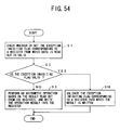
FIG. 54 is a flowchart showing an
operation in accordance with an arithmetic operation
instruction in the twelfth embodiment;
FIG. 55 is a flowchart showing an
operation in accordance with an exception inhibiting
load instruction in the twelfth embodiment;
FIG. 56 shows the structure of a processor
in accordance with a thirteenth embodiment of the
present invention;
FIG. 57 shows the structure of an
arithmetic operation instruction execution unit
shown in FIG. 56;
FIG. 58 is a flowchart showing an
operation performed by the processor of FIG. 56 when
a data break is detected;
FIG. 59 is a flowchart showing an
operation performed by the processor of FIG. 56 when
the execution of an instruction is ensured in the
inherent order;
FIG. 60 is a flowchart showing an
operation performed by the processor of FIG. 56 in
accordance with an interrupt operation program in a
data break interrupt operation;
FIG. 61 is a flowchart showing an
operation performed by the processor of FIG. 56 when
a software break interrupt operation in accordance
with an interrupt operation program;
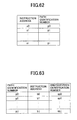
FIG. 62 shows the structure of an
exception inhibiting load instruction table of the
thirteenth embodiment of the present invention;
FIG. 63 shows the structure of a commit
point table in accordance with the thirteenth
embodiment of the present invention;
FIG. 64 shows the structure of a commit
break point table in accordance with the thirteenth
embodiment of the present invention;
FIG. 65 shows the structure of an
exception inhibiting data break history table in
accordance with the thirteenth embodiment of the
present invention;
FIG. 66 shows the structure of a processor
in accordance with a fourteenth embodiment of the
present invention;
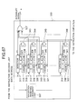
FIG. 67 shows the structure of a data
break detector unit shown in FIG. 66;
FIG. 68 shows the structure of a history
control unit shown in FIG. 66;
FIG. 69 is a flowchart showing a data
break interrupt operation performed by the processor
of FIG. 66 in accordance with an interrupt operation
program;
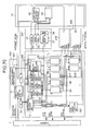
FIG. 70 shows the structure of a processor
in accordance with a fifteenth embodiment of the
present invention;
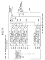
FIG. 71 shows the structure of a data
break detector point shown in FIG. 70;
FIG. 72 shows the structure of a break
history control unit shown in FIG. 70;
FIG. 73 shows the structure of a processor
in accordance with a sixteenth embodiment of the
present invention;
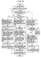
FIG. 74 is a flowchart showing a data
break interrupt operation performed by a processor
of FIG. 73 in accordance with an interrupt operation
program; and
FIG. 75 shows the structure of an
exception inhibiting data break history table in
accordance with the sixteenth embodiment of the
present invention.
DESCRIPTION OF THE PREFERRED EMBODIMENTS
The following is a description of
embodiments of the present invention, with reference
to the accompanying drawings. In the drawings, the
same components are denoted by the same reference
numerals.
A processor of the present invention
executes a programmed instruction
[First Embodiment]
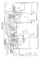
FIG. 13 shows the structure of a processor
in accordance with a first embodiment of the present
invention. As shown in FIG. 13, the processor of
this embodiment is the same as the conventional
processor shown in FIG. 1, except that the processor
of this embodiment further comprises a history
control unit 51, and an instruction execution unit
41 comprises a speculative load instruction
execution unit 43, an interference recovery store
instruction execution unit 45, and a load history
reset unit 47.
The input terminal of the speculative load
instruction execution unit 43 is connected to a
decoder unit 42 and a memory unit 1. The output
terminal of the speculative load instruction
execution unit 43 is connected to the general
register 37, a speculative load operating history
control unit 51, and an interrupt control circuit 55.
The input terminal of the interference recovery
store instruction execution unit 45 is connected to
the decoder unit 42, the general register 37, and
the history control unit 51. The output of the
interference recovery store instruction execution
unit 45 is connected to the memory 1, the general
register 37, the history control unit 51, and the
interrupt control circuit 55. The input terminal of
the load history reset unit 47 is connected to the
decoder unit 42, while the output terminal is
connected to the history control unit 51.
FIG. 15 is a flowchart of an operation
performed in accordance with a speculative load
instruction. When the speculative load instruction
execution unit 43 receive a speculative load
instruction from the decode unit 42, the speculative
load instruction execution unit 43 determines an
effective address from a value read out from the
general register 37. As shown in FIG. 15, the
speculative load instruction execution unit 43 reads
out data from the region in the memory 1
corresponding to the effective address, and then
writes the data in the general register 37 in step
S1. In step S2, the speculative load instruction
execution unit 43 supplies the history control unit
51 with a registration signal ADD for registering
the execution of the speculative load instruction,
and the history control unit 51 registers the
history of load operations in a load operation
history table in step S2. As shown in FIG. 16, the
format of the speculative load instruction is the
same as the format of the load instruction shown in
FIG. 3. In a case where the speculative load
instruction execution unit 43 detects an interrupt
when executing the speculative load instruction, the
speculative load instruction execution unit 43
supplies an interrupt signal to the interrupt
control circuit 55.
FIG. 17 is a flowchart showing an
operation performed in accordance with an
interference recovery store instruction.
When the interference recovery store
instruction execution unit 45 receives an
interference recovery store instruction from the
decoder unit 42, the interference recovery store
instruction execution unit 45 determines an
effective address from a value read out from the
general register 37, and, at the same time, supplies
a confirmation signal CC to the history control unit
51. In step S1, the history control unit 51 checks
whether or not the two address regions for
speculative load operations registered in the store
operation history table and the speculative load
operation history table interfere (or overlap) with
each other.
In step S2, it is determined whether or
not the above interference exists. If there is no
interference, the operation moves on to step S3 in
which the interference recovery store instruction
execution unit 45 writes data read out from the
general register 37 in the region in the memory 1
corresponding to the effective address. If it is
determined that the two address regions interfere
with each other, the operation moves on to step S10
in which the interference recovery store instruction
execution unit 4 refers to the load operation
history table, and rewrites store data in a load
register designated as a store destination by the
speculative load operation. After that, the
operation moves on to step S3, in which the
interference recovery store instruction execution
unit 45 writes data read out from the general
register 37 into the region in the memory 1
corresponding to the effective address.
As shown in FIG. 18, the format of the
instruction is the same as the format of the store
instruction shown in FIG. 5. If the interference
recovery store instruction execution unit 45 detects
an interrupt when executing the interference
recovery store instruction, the interference
recovery store instruction execution unit 45
supplies an interrupt signal to the interrupt
control circuit 55.
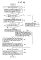
FIG. 19 is a flowchart showing an
operation performed in accordance with a speculative
load operation history nullifying instruction. As
shown in FIG. 19, when the load history reset unit
47 receives the speculative load operation history
nullifying instruction from the decoder unit 42, the
load history reset unit 47 supplies reset signal RS
to the history control unit 51, thereby nullifying
all the entries in the speculative load operation
history table. As shown in FIG. 20, the format of
the speculative load operation history nullifying
instruction is made up of only an instruction code
OP-CODE.
FIG. 14 shows the structure of the history
control unit 51 shown in FIG. 13. As shown in FIG.
14, the history control unit 51 comprises an address
register 57, a data type register 59, a register
number register 61, a store data register 63, a
decoder circuit 65, comparators 67 to 69, E fields
70, 74, and 78, address fields 71, 75, and 79, data
type fields 72, 76, and 80, register number fields
73, 77, and 81, an overlap judgment unit 83, an
overlap entry detector unit 85, an invalid entry
detector unit 87, a speculative load operation
history reset control unit 89, a speculative load
operation history registration control unit 91, and
a speculative load operation history interference
confirmation control unit 93.
As shown in FIG. 14, the instruction
execution unit 41 is connected to the address
register 57, the data type register 59, the register
number register 61, the store data register 63, and
the decoder circuit 65. The address register 57
holds an effective address used for executing the
speculative load instruction or the interference
recovery store instruction. The data type register
59 holds an identification value that represents the
size of data to be loaded or stored in the execution
of the speculative load instruction or the
interference recovery store instruction. The
register number register 61 holds the register
number of a register to be loaded or stored in the
execution of the speculative load instruction or the
interference recovery store instruction.
The store data register 63 holds a write
value (store data) in accordance with the
interference recovery store instruction. The
decoder circuit 65 analyzes a signal supplied from
the instruction execution unit 41, and activates the
corresponding control unit. More specifically, when
the registration signal ADD is supplied, the store
data register 63 activates the speculative load
operation history registration control unit 91.
When the confirmation signal CC is supplied, the
store data register 63 activates the speculative
load operation history interference confirmation
control unit 93. When the reset signal RS is
supplied, the store data register 63 activates the
speculative load operation history reset control
unit 89.
Meanwhile, the comparators 67 to 69 are
connected to the entries corresponding to the
address register 57 and the data type register 59.
Here, the speculative load operation history table
is made up of a plurality of entries. Each of the
entries includes the E fields 70, 74, and 78 that
represent effectiveness, the address fields 71, 75,
and 79 that represent the effective addresses of
registered speculative load operations, the data
type fields 72, 76, and 80 that represent the type
of data subjected to registered speculative load
operations, and the register number fields 73, 77,
and 81 that represent the register number of
registered to be loaded in the registered
speculative load operations. In the data type
fields 72, 76, and 80, identification values
corresponding to the type of data are recorded. The
identification value for an unsigned byte is 0; the
identification value for a signed byte is 1; the
identification value for an unsigned half word is 2;
the identification value for a signed half word 3;
the identification value for a word is 4; the
identification value for a double word is 5; and the
identification value for a quad word is 6.
The comparators 67 to 69 compare the
address region of load data determined by the
address fields 71, 75, and 79, and the data type
fields 72, 76, and 80, with the address region of
store data determined by the address register 57 and
the data type register 59, and each output a signal
indicating whether or not the two address regions
interfere (overlap) with each other.
The overlap judgment unit 83 is connected
to the comparators 67 to 69. In accordance with
signals supplied from the comparators 67 to 69, the
overlap judgment unit 83 determines whether or not
the address region for the speculative load
operation registered as the speculative load
operation history overlaps with the address region
for the store operation in accordance with the
interference recovery store instruction. If the two
address regions overlap with each other , the
overlap judgment unit 83 outputs an overlap signal
OL. The overlap entry detector unit 85 is connected
to the comparators 67 to 69, and, in accordance with
the signals supplied from the comparators 67 to 69,
the overlap entry detector unit 85 detects the
numbers of entries that are subjected to the
speculative load operation and interfere with each
other.
In accordance with the information of the
E fields 70, 74, and 78 of each entry, the invalid
entry detector unit 87 detects a dead entry (invalid
entry) in the speculative load operation. The
speculative load operation history reset control
unit 89 is connected to the decoder circuit 65,
thereby resetting the E fields 70, 74, and 78 of
each entry to 0.
The speculative load operation history
registration control unit 91 is connected to the
address register 57, the data type register 59, the
register number register 61, the decoder circuit 65,
and the invalid entry detector unit 87. In
accordance with a supplied registration signal ADD,
the speculative load operation history registration
control unit 91 writes the information corresponding
to the speculative load operations in the address
fields 71, 75, and 79, the data type fields 72, 76,
and 80, and the register number fields 73, 77, and
81 of the dead entries detected by the invalid entry
detector unit 87. Here, the value "1" indicating
validity is written in each of the E fields 70, 74,
and 78 of the entries in which the information has
been written.
The speculative load operation history
interference confirmation control unit 93 is
connected to the address register 57, the data type
register 59, the register number register 61, the
store data register 63, the overlap judgment unit 83,
the overlap entry detector unit detector unit 85,
the decoder circuit 65, and the general register 37.
The information of the register number fields 73, 77,
and 81 is supplied to the speculative load operation
history interference confirmation control unit 93.
In a case where the overlap judgment unit 83
determines that there is an overlap, the speculative
load operation history interference confirmation
control unit 93 writes a write value (store data) by
a store operation in the register in which the data
is stored. The value written in the register is a
value obtained by performing a sign extension
process or a zero extension process on the store
data, based on the information in the data type
fields 72, 76, and 80.
Next, the operation of the above process
will be summarized. In the initial stage, a normal
operation is performed. In the normal operation,
the instruction read unit 3 reads an instruction
word indicated by the program counter 13, and then
supplies the instruction word to the instruction
execution unit 41. The instruction execution unit
41 in turn executes the supplies instruction.
However, if the instruction execution unit 41
receives a speculative load instruction, the
instruction execution unit 41 additionally registers
the history of the load operation in the history
control unit 51.
In a case where an interference recovery
store instruction is supplied, the address of data
subjected to the store operation is checked whether
or not to interfere with the address region of the
data already subjected to the previous speculative
load operation and registered in the history control
unit 51. If there is interference, the store data
is written in the register in which the interfering
data is already stored, thereby restoring the data
from the disorder caused by the interference. In
the normal operation, the above operation is
repeated.
In a case where an interrupt occurs, in
accordance with an interrupt signal supplied from
the instruction read unit 3 or the instruction
execution unit 41, the interrupt control circuit 55
writes the address of an instruction word that is
the return destination from the interrupt, in the
register 31, also writes the pre-interrupt operation
state in the register 33, and further writes the
operation state corresponding to the interrupt in
the register 35. Also, the branch destination
address corresponding to the interrupt is supplied
to the program counter 13. Here, the instruction
read unit 3 reads an instruction word from the
memory 1 in accordance with the supplied branch
destination address, and then supplies the
instruction word to the instruction execution unit
41. After that, the operation is continued in the
same manner as in the above-described normal
operation.
When performing interrupt return, the
instruction execution unit 41 executes an interrupt
return instruction, thereby writing the value from
the register 33 into the register 53. The
instruction execution unit 41 also reads out the
value from register 31 and supplies the value as the
branch destination address to the instruction read
unit 3. Here, the instruction read unit 3 reads out
an instruction word from the memory 1 in accordance
with the supplied branch destination address, and
supplies the instruction word to the instruction
execution unit 41. After that, the operation is
continued in the same manner as in the normal
operation.
In accordance with the above-described
first embodiment of the present invention, when the
address region of data subjected to an operation in
accordance with a speculative load instruction
previously executed overlaps with the address region
of data subjected to an operation in accordance with
an interference recovery store instruction executed
later, store data is written over the interfering
data, so that ambiguous reference to the memory can
be avoided in the execution of the load operation
prior to the store operation. Thus, a precise and
high-speed operation can be performed.
[Second Embodiment]
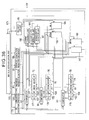
FIG. 21 shows the structure of a processor
in accordance with a second embodiment of the
present invention. As shown in FIG. 21, the
processor of the second embodiment has the same
structure as the processor of the first embodiment
shown in FIG. 13, except that the instruction
execution unit 41 further comprises a speculative
load operation history read instruction execution
unit 95 and a speculative load operation history
write instruction execution unit 97, and a history
control unit 103 has a different structure from the
history control unit 51. The processor of this
embodiment also differs from the first embodiment in
that the instruction execution unit 41 comprises a
floating point load instruction execution unit 25, a
floating point store instruction execution unit 27,
and a floating point calculation instruction
execution unit 29, which are accompanied by a
speculative floating point load instruction
execution unit 99 and an interference recovery
floating point store instruction execution unit 101.
Here, the speculative load operation
history read instruction execution unit 95 is
connected to the instruction decoder unit 94, the
general register 37, and the history control unit
013. The speculative load operation history write
instruction execution unit 97 is connected to the
general register 37 and the history control unit 103.
The speculative floating point load instruction
execution unit 99 and the interference recovery
floating point store instruction execution unit 101
are connected to the instruction decoder unit 94,
the floating point load instruction execution unit
25, the floating point register 39, the interrupt
control circuit 40, and the history control unit 103.
FIG. 22 shows the structure of the history
control unit 103 shown in FIG. 21. As shown in FIG.
22, the history control unit 103 has the same
structure as the history control unit 51 shown in
FIG. 14, except that the history control unit 103
further comprises a register type register 105, a
speculative load operation history read instruction
execution unit 113, and a speculative load operation
history write instruction execution unit 115. Here,
each entry includes register type fields 107 to 109
that represent the types of registers.
The register type register 105 is
connected to an instruction execution unit 100. The
speculative load operation history read instruction
execution unit 113 is connected to the address
register 57, each of the entries, a decoder circuit
111, and the instruction execution unit 100. The
speculative load operation history write instruction
execution unit 115 is connected to the address
register 57, the data type register 59, the register
type register 105, the register number register 61,
the decoder circuit 11, and each of the entries.
In the above structure, when receiving a
speculative load operation history read instruction
from the instruction decoder unit 94, the
speculative load operation history read instruction
execution unit 95 supplies a history read signal HR
to the history control unit 103, and then writes the
read history of the speculative load operation into
the general register 37. When receiving a
speculative load operation history write instruction
from the instruction decoder unit 94, the
speculative load operation history read instruction
execution unit 95 supplies the data read out from
the general register 37, as well as a history write
signal HW, to the history control unit 103.
Based on a registration signal ADD
supplied from the speculative load instruction
execution unit 43 or the speculative floating point
load instruction execution unit 99, the history
control unit 103 registers the speculative load
operation in the speculative load operation history
table. In accordance with a confirmation signal CC
supplied from the interference recovery store
instruction execution unit 45 and the interference
recovery floating point store instruction execution
unit 101, the history control unit 103 checks
whether or not the store operation by an
interference recovery store instruction or an
interference recovery floating point store
instruction interferes with the address region for
the operation in the speculative load operation
registered in the speculative load operation history
table. If the address regions interferes with each
other, a write value (store data) obtained from the
execution of the interference recovery store
instruction or the interference recovery floating
point store instruction is written as the load
destination of a next speculative load operation
over the interfering data in the register.
In accordance with the history read signal
HR supplied from the speculative load operation
history read instruction execution unit 95, the
speculative load operation history read instruction
execution unit 113 reads out the history of the
speculative load operation from the load operation
history table, and supplies the history of the
speculative load operation to the speculative load
operation history read instruction execution unit 95.
Furthermore, in accordance with the history write
signal HW supplied from the speculative load
operation history write instruction execution unit
97, the speculative load operation history write
instruction execution unit 115 writes the data
supplied from the speculative load operation history
write instruction execution unit 97 into the
speculative load operation history table.
The register type register 105 shown in
FIG. 22 holds identification values for identifying
registers to be operated in the execution of the
instructions, i.e., the speculative load instruction,
the interference recovery store instruction, the
speculative floating point load instruction, and the
interference recovery floating point store
instruction. The identification value for a general
register is 0, while the identification value for a
floating point register is 1. The register type
fields 107 to 109 holds setting values that
represent the types of registers subjected to the
speculative load operation.
With the processor of the second
embodiment described above, the same effects as in
the first embodiment can be obtained, and the
speculative load operation history table can be
arbitrarily rewritten. Thus, context switching can
be easily carried out.
Also, by holding the information
representing the types of registers as a history, a
preceding operation for the general register can be
distinguished from an operation for the floating
point register 39. Thus, ambiguous reference to the
memory can be avoided in the data processing in both
registers, and a precise and high-speed operation
can be performed.
[Third Embodiment]
FIG. 23 shows the structure of a processor
in accordance with a third embodiment of the present
invention. A shown in FIG. 23, the processor of the
third embodiment has the same structure as the
processor of the second embodiment shown in FIG. 21,
except that an instruction execution unit 120
comprises a context identification number register
read instruction execution unit 119 and a context
identification number register write instruction
execution unit 121, in place of the floating point
load instruction execution unit 25, the floating
point store instruction execution unit 27, the
floating point calculation instruction execution
unit 29, the speculative floating point load
instruction execution unit 99, and the interference
recovery floating point store instruction execution
unit 101.
A register control unit 123 comprises a
context identification number register 125 in place
of the floating point register 39. An interrupt
control unit 129 further comprises an overflow
exception interrupt control unit 131. Furthermore,
with the above components, the structure of a
history control unit 127 is changed accordingly.
The context identification number register
read instruction execution unit 119 and the context
identification number register write instruction
execution unit 121 are connected to the instruction
decoder unit 117, the general register 37, the
history control unit 127, and the context
identification number register 125. The contest
identification number register 125 is connected to
the history control unit 127. The overflow
exception interrupt control unit 131 is connected to
the program counter 13, the registers 31, 33, and 35,
and the history control unit 127.
FIG. 24 shows the structure of the history
control unit 127 shown in FIG. 23. As shown in FIG.
24, the history control unit 127 has the same
structure as the history control unit 103 shown in
FIG. 22, except that the history control unit 127
further comprises an overflow judgment unit 139, and
each entry includes context identification fields
135 to 137 in place of the register type fields 107
to 109. The overflow judgment unit 139 is supplied
with the values of the E fields 70, 74, and 78 of
each entry.
Here, the context identification number
register 125 holds an identification number for
identifying a current context. When receiving a
context identification number register read
instruction from the instruction decoder unit 117,
the context identification number register read
instruction execution unit 119 reads out a context
identification number from the context
identification number register 125, and then writes
the context identification number in the general
register 37. When receiving a context
identification number register write instruction
from the instruction decoder unit 117, the context
identification number register write instruction
execution unit 121 writes the data read out from the
general register 37 into the context identification
number register 125.
When receiving an overflow signal OF from
the history control unit 127, the overflow execution
interrupt control unit 131 generates an interrupt,
and then writes the interrupt return address in the
register 31, the pre-interrupt operation state in
the register 33, and the operation state of the
interrupt in the register 35. Also, the overflow
execution interrupt control unit 131 supplies the
branch destination address corresponding to the
interrupt to the program counter 13.
The overflow judgment unit 139 determines
whether or not a free entry in which registration
can be performed exists in the speculative load
operation history table. More specifically, an
entry having the E fields 70, 74, and 78 provided
with the value "0" is determined to be a free entry.
The overflow judgment unit 319 then notifies the
speculative load operation history registration
control unit 91 of the presence or absence of a free
entry. When there is no free entry, the overflow
judgment unit 139 supplies the overflow signal OF to
the overflow exception interrupt control unit 131.
In the processor of the third embodiment
described above, when the values of the context
identification fields 135 to 137 coincide with the
context identification numbers supplied from the
context identification number register 125 in
entries having the E fields 70, 74, and 78 provided
with the value "1", the comparators 132 to 134 are
activated, and the presence or absence of the
interference is determined. Thus, ambiguous
reference to the memory can be avoided, and a
precise and high-speed operation can be performed.
Also, the context identification numbers
stored in the context identification number register
125 can be freely rewritten. Thus, context
switching can be easily carried out.
[Fourth Embodiment]
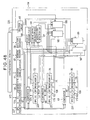
FIG. 25 shows the structure of a processor
in accordance with a fourth embodiment of the
present invention. As shown in FIG. 25, the
processor of the fourth embodiment has the same
structure as the process of the first embodiment
shown in FIG. 13, except that an instruction
execution unit 145 of this embodiment comprises the
speculative load operation history read instruction
execution unit 95, and further comprises a store
data table read instruction execution unit 143. The
processor of this embodiment also differs from the
first embodiment in that an interrupt control unit
150 comprises an interference recovery exception
interrupt control unit 149.
Here, the store data table read
instruction execution unit 143 is connected to an
instruction decoder unit 141, a history control unit
147, and the general register 37. The interference
recovery exception interrupt control unit 149 are
connected to the program counter 13, the registers
31, 33, and 35, and the history control unit 147.
With the above components, the structure
of the history control unit 147 is changed
accordingly. FIG. 26 shows the structure of the
history control unit 147 shown in FIG. 25. As shown
in FIG. 26, the history control unit 147 has the
same structure as the history control unit 51 shown
in FIG. 14, except that the history control unit 147
of this embodiment further comprises the speculative
load operation history read instruction execution
unit 113, a store data table read instruction
execution unit 157, and data fields DATAO to DATAm.
Also, each entry includes V fields 151 to 153 and
entry fields 154 to 156.
Here, the store data table read
instruction execution unit 157 is connected to the
address register 57, the data fields DATAO to DATAm,
the decoder circuit 65, and the instruction
execution unit 41.
In the processor having the above
structure, in accordance with a store data table
read instruction supplied from the instruction
decoder unit 141, the store data table read
instruction execution unit 143 supplies a store data
read signal SR to the history control unit 147,
thereby reading a store data table described later
and writing the read data into the general register
37.
In accordance with an overlap signal OL
supplied from the history control unit 147, the
interference recover exception interrupt control
unit 149 generates an interrupt, and writes an
interrupt return address in the register 31, the
pre-interrupt operation state in the register 33,
and the operation state corresponding to the
interrupt in the register 35. The interference
recovery exception interrupt control unit 149 also
supplies a branch destination address corresponding
to the interrupt to the instruction read unit 3.
In accordance with a store data read
signal SR supplied from the store data table read
instruction execution unit 143, the history control
unit 147 reads the store data table, and then
supplies the read data to the store data table read
instruction execution unit 143.
The data in the V fields 151 to 153 shown
in FIG. 26 indicates whether or not the address
region subjected to the speculative load operation
in the corresponding entry interferes with the
address region subjected to the store operation by
an interference recovery exception store instruction.
For instance, in a case where the data in the V
fields 151 to 153 is "0", there is no interference.
On the other hand in a case where the data in the V
fields 151 to 153 is "1", the two address regions
interferes with each other.
The entry fields 154 to 156 represent the
entry numbers of the store data table that holds
write values (store data) in accordance with the
interference recovery exception store instruction
when the corresponding one of the V fields 151 to
153 is "1". In an interference recovery exception
interrupt operation program mentioned later,
recovery is carried out with reference to the entry
fields 154 to 156.
The data fields DATA0 to DATAm constitute
the entry of the store data table, and holds write
values (store data) of an interfering store
operation in a case where the address region of the
speculative load operation registered in the
speculative load operation history table interferes
with the address region subjected to the store
operation in accordance with the interference
recovery exception store instruction.
Next, the operation of the processor of
the fourth embodiment having the above structure
will be described below. In the initial stage, a
normal operation is performed. In the normal
operation, the instruction read unit 3 reads out an
instruction word indicated by the program counter 13,
and supplies the instruction word to the instruction
execution unit 145. The instruction execution unit
145 normally executes a supplied instruction.
However, when receiving a speculative load
instruction, the instruction execution unit 145
additionally registers the history of the load
operation in the history control unit 147.
FIG. 27 is a flowchart showing the
operation in a case where the interference recovery
exception store instruction is supplied. In step S1,
it is determined whether or not the address of data
subjected to the store operation interferes with the
address region of data that has been subjected to a
previous speculative load operation and already
registered in the history control unit 147. If
there is interference in step S2, the operation
moves on to step S10, in which the store data is
additionally written in the store table, and the
interrupt operation program of the interference
recovery exception is executed.
FIG. 29 is a flowchart showing the
interrupt operation program of the interference
recovery exception. In the interrupt operation
program of the interference recovery exception, the
context is saved in step S1, and the store data is
written in the register of a load destination in the
interfering load operation, with reference to the
load operation history table and the store data
table in step S2. The context is then restored in
step S3, and an interrupt return instruction is
executed in step S4.
Meanwhile, if there is no interference in
step S2 in FIG. 27, the operation moves on to step
S3, in which the data read out from the general
register 37 is written as the data of the store
object address region. If a store data table read
instruction is supplied, predetermined store data is
read out from the store data table. In the normal
operation, these steps are repeated. The format of
the interference recovery exception store
instruction shown in FIG. 28 is the same as the
format of the store instruction shown in FIG. 5.
When an interrupt occurs, in accordance
with an interrupt signal supplied from the
instruction read unit 3 or the instruction execution
unit 145, the interrupt control circuit 40 writes
the address of an instruction word at the return
destination from the interrupt into the register 31,
the pre-interrupt operation state into the register
33, and the operation state corresponding to the
interrupt into the register 35. The interrupt
control circuit 40 also supplies the branch
destination address corresponding to the interrupt
to the program counter 13. In accordance with the
supplied branch destination address, the instruction
read unit 3 reads out an instruction word from the
memory 1, and supplies the instruction word to the
instruction execution unit 145. After that, the
operation returns to the normal operation.
When a return operation from the interrupt
is performed, the instruction execution unit 145
executes an interrupt return instruction so as to
write the value read out from the register 33 into
the register 35. The instruction execution unit 145
also reads out the value from the register 31, and
supplies the value as a branch destination address
to the instruction read unit 3. In accordance with
the supplied branch destination address, the
instruction read unit 3 reads out an instruction
word from the memory 1, and supplies the instruction
word to the instruction execution unit 41. After
that, the operation returns to the normal operation
described above.
As described so far, with the processor of
the fourth embodiment, data disorder due to
interference can be corrected by a data processing
operation. Thus, the same effects as with the
processor of the first embodiment can be easily
obtained.
[Fifth Embodiment]
In the history control unit 147 of the
processor of the fourth embodiment shown in FIG. 26,
it is also possible to arrange the V fields 151 to
153 and the entry fields 154 to 156 in contact with
the data fields DATA0 to DATAm.
FIG. 30 shows the structure of a history
control unit 159 of a processor in accordance with
the a fifth embodiment of the present invention. As
shown in FIG. 30, V fields Vn (n = 0 to m) and entry
fields ENTn are arranged adjacent to data fields
DATAn. With this structure, the same effects as
with the processor of the fourth embodiment can be
obtained.
[Sixth Embodiment]
FIG. 31 shows the structure of a processor
in accordance with a sixth embodiment of the present
invention. As shown in FIG. 24, the processor of
this embodiment has the same structure as the
processor of the fourth embodiment shown in FIG. 25,
except that an instruction execution unit 165
comprises an interference recovery branching store
instruction execution unit 161 and an interference
recovery branch address register write instruction
execution unit 163, in place of the interference
recovery store instruction execution unit 45. Also,
a register control unit 169 of the processor of this
embodiment further comprises an interference
recovery branch address register 167.
The interference recovery branching store
instruction execution unit 161 is connected to the
instruction decoder unit 141, the general register
37 the interrupt control circuit 40, and a history
control unit 148. The interference recovery branch
address register write instruction execution unit
163 is connected to the instruction decoder unit 141,
the general register 37, and the interference
recovery branch address register 167. The
interference recovery branch address register 167 is
connected to the history control unit 148.
FIG. 32 shows the structure of the history
control unit 148 shown in FIG. 31. As shown in FIG.
32, the history control unit 148 of this embodiment
has the same structure as the history control unit
147 shown in FIG. 26, except that the speculative
load operation history interference confirmation
control unit 93 is connected to the interference
recovery branch address register 167 and the program
counter 13.
When receiving an interference recovery
branching store instruction from the instruction
decoder unit 17, the interference recovery branching
store instruction execution unit 161 determines an
effective address from a value read out from the
general register 37, and writes the data read out
from the general register 37 into the region in the
memory 1 corresponding to the effective address.
The interference recovery branching store
instruction execution unit 161 also outputs a
confirmation signal CC to the history control unit
148. In a case where an interrupt has been detected
at the time of executing an instruction, an
interrupt signal is supplied to the interrupt
control circuit 40.
When receiving an interference recovery
branch address register write instruction from the
instruction decoder unit 17, the interference
recovery branch address register write instruction
execution unit 163 writes the data read out from the
general register 37 into the interference recovery
branch address register 167. The interference
recovery branch address register 167 holds a first
address of a recovery code for recovering from data
disorder due to interference.
Next, the operation of the processor
having the above structure will be described. In
the initial state, a normal operation is performed.
In the normal operation, the instruction read unit 3
reads out an instruction word indicated by the
program counter 13, and supplies the instruction
word to the instruction execution unit 165. The
instruction execution unit 165 normally performs a
supplied instruction. However, the instruction
execution unit 165 additionally registers the
history of the load operation in the history control
unit 148.
FIG. 33 is a flowchart showing the
operation when the interference recovery branching
store instruction is supplied. In step S1, it is
determined whether or not the address of data
subjected to the store operation interferes with the
address region of the data that has been subjected
to a previous speculative load operation and already
registered in the history control unit 148. If
there is interference in step S2, the operation
moves on to step S10, in which the store data is
added to the store data table, and branching is
carried out to an instruction address indicated by
the interference recovery branch address register
167.
If there is no interference in step S2,
the operation moves on to step S3, in which the data
read out from the general register 37 is written as
the data of the store object address region. In the
normal operation, these steps are repeated. The
format of the interference recovery branching store
instruction shown in FIG. 34 is the same as the
format of the store instruction shown in FIG. 5.
When a store data table read instruction is supplied,
the store data is read out from the store data table.
When an interrupt occurs, in accordance
with a interrupt signal supplied from the
instruction read unit 3 or the instruction execution
unit 165, the interrupt control circuit 40 writes
the address of an instruction word of a return
destination from the interrupt into the register 31,
the pre-interrupt operation state into the register
33, and the operation state corresponding to the
interrupt into the register 35. The interrupt
control circuit 40 also supplies the branch
destination address corresponding to the interrupt
to the program counter 13. Here, the instruction
read unit 3 reads out an instruction word from the
memory 1 in accordance with a supplied branch
destination address, and supplies the instruction
word to the instruction execution unit 165. After
that, the operation returns to the normal operation.
When returning from an interrupt, the
instruction execution unit 165 executes an interrupt
return instruction, thereby writing the value read
out from the register 33 into the register 35. The
instruction execution unit 165 also reads out the
value from the register 31, and supplies the value
as the branch destination address to the instruction
read unit 3. Here, the instruction read unit 3
reads out an instruction word from the memory 1 in
accordance with the supplied branch destination
address, and supplies the instruction word to the
instruction execution unit 41. After that, the
operation returns to the normal operation.
As described above, with the processor of
the sixth embodiment, it is possible to recover from
data disorder due to interference by a program at a
branch destination designated through the execution
of a branch instruction. Thus, the same effects as
with the processor of the first embodiment can be
achieved with a simpler structure.
In the processor of the sixth embodiment,
there is no need to perform operations, such as the
context saving and restoring, at the time of
recovery. Thus, the data processing rate can be
further increased.
[Seventh Embodiment]
FIG. 35 shows the structure of a processor
in accordance with a seventh embodiment of the
present invention. As shown in FIG. 35, the
processor of this embodiment has the same structure
as the conventional processor shown in FIG. 6,
except that the processor of this embodiment further
comprises a history control unit 173. The processor
of this embodiment differs from the processor shown
in FIG. 6 also in that an instruction execution unit
170 comprises an exception inhibiting load
instruction execution unit 24, a commit instruction
execution unit 26, an exception inhibiting history
read instruction execution unit 28, and an exception
inhibiting history write instruction execution unit
20, that a register control unit 171 further
comprises an exception inhibiting flag 38, and that
an interrupt control unit 10 further comprises a
commit exception interrupt control unit 44.
The history control unit 173 is connected
to the exception inhibiting history write
instruction execution unit 20, the exception
inhibiting load instruction execution unit 24, the
commit instruction execution unit 26, the exception
inhibiting history read instruction execution unit
28, and the commit exception interrupt control unit
44. The exception inhibiting history write
instruction execution unit 20, the commit
instruction execution unit 26, and the exception
inhibiting history read instruction execution unit
28 are also connected to the instruction decoder
unit 17 and the general register 37. The
exceptional inhibiting load instruction execution
unit 24 is also connected to the memory 1.
The exception inhibiting flag 38 is
attached to the general register 37. The commit
exception interrupt control unit 44 is also
connected to the program counter 13 and the
registers 31, 33, and 35.
When receiving an exception inhibiting
load instruction, the exception inhibiting load
instruction execution unit 24 determines an
effective address from a value read out from the
general register 37, and reads out data from the
region in the memory 1 corresponding to the
effective address. As shown in FIG. 37, it is
determined whether or not an exception factor exists
in the read out data in step S1. If it is
determined that there is no exception factor in step
S2, the operation moves on to step S3, in which the
data read out from the load object address region
into the general register 37.
If it is determined that there is an
exception factor in step S2, the operation moves on
to step S10, a registration command signal is
supplied to the history control unit 173, thereby
storing the detected exception information in the
history control unit 173. In step S11, the
exception inhibiting flag 38 corresponding to the
register, in which the exception information is
stored, is set to the value "1", thereby indicating
its effectiveness. The format of the exception
inhibiting load instruction is the same as the
format of the load instruction shown in FIG. 3.
When receiving a commit instruction, the
commit instruction execution unit 26 determines
whether or not the exception inhibiting flag 38
corresponding to the register designated by the
commit instruction is effective in step S1 shown in
FIG. 38. If the exception inhibiting flag 38 is
determined to be effective in step S2, the operation
moves on to step S3, in which the exception
inhibiting flag 38 is set at "0" that indicating
invalidity. In step S4, a confirmation command
signal is supplied to the history control unit 173,
thereby notifying the interrupt control unit 10 that
the commit exception occurs. If the exception
inhibiting flag 38 is determined to be invalid in
step S2, the operation by the commit instruction
comes to an end. The format of the commit
instruction is made up of an instruction code OP-CODE
and a code GR for designating a register, as
shown in FIG. 39.
When receiving an exception inhibiting
history read instruction, the exception inhibiting
history read instruction execution unit 28 supplies
a read command signal to the history control unit
173, thereby reading out the exception information
from the history control unit 173 and writing the
exception information into the general register 37.
Likewise, when receiving an exception inhibiting
history write instruction, the exception inhibiting
history write instruction execution unit 20 supplies
the history control unit 173 with data read out from
the general register 37 and a write command signal,
and writes the read out data in the history control
unit 173.
In response to a interrupt-notifying
commit signal CM supplied from the history control
unit 173, the commit exception interrupt control
unit 44 writes an instruction address of a return
destination from an interrupt into the register 31,
data indicating the pre-interrupt operation state
into the register 33, and the operation state
corresponding to the interrupt into the register 35.
The commit exception interrupt control unit 44
supplies a branch destination address corresponding
to the interrupt to the program counter 13.
In response to a confirmation command
signal supplied from the commit instruction
execution unit 26, the history control unit 173
checks whether or not any exception information is
held in the register of a designated register number.
If there is exception information held in the
register of the designated register number, a commit
signal CM indicating that a commit exception has
been detected is supplied to the commit exception
interrupt control unit 44.
In response to a read command signal
supplied from the exception inhibiting history read
instruction execution unit 28, the history control
unit 173 reads out stored exception information, and
supplies the exception information to the exception
inhibiting history read instruction execution unit
28. Furthermore, in accordance with a write command
signal supplied from the exception inhibiting
history write instruction execution unit 20, the
history control unit 173 stores supplied data.
FIG. 36 shows the structure of the history
control unit 173. As shown in FIG. 36, the history
control unit 173 comprises the address register 57,
the data type register 59, the register number
register 61, an exception factor register 175, the
register type register 105, the decoder circuit 65,
the comparators 67 to 69, EC fields (EC) 177 to 179,
the V fields 151 to 153, the register type fields
(RT) 107 to 109, the address fields (ADDR) 71, 75,
and 79, the data type fields (DT) 72, 76, and 80,
the register number fields (REG#) 73, 77, and 81, a
commit judgment unit 180, a commit entry detector
unit 181, the invalid entry detector unit 877, an
exception inhibiting history registration control
unit 183, a commit instruction execution unit 185,
an exception inhibiting history read instruction
execution unit 187, and an exception inhibiting
history write instruction execution unit 189.
The address register 57, the data type
register 59, the register number register 61, the
register type register 105, the EC register 175, and
the decoder circuit 65 are connected to the
instruction execution unit 170. The address
register 57 holds an effective address for executing
an exception inhibiting load instruction. The data
type register 59 holds an identification value
indicating the size of data subjected to a
load/store operation in the execution of the
exception inhibiting load instruction. The register
number register 61 holds the register number of a
register subjected to a write operation in the
execution of the exception inhibiting load
instruction.
The
register type register 105 holds an
identification value indicating the type of a
register to be operated. The EC register 175 holds
an identification value of an exception factor
detected in the execution of the exception
inhibiting load instruction. Examples of exception
factors and identification values are shown in Table
1.
| Exception factor | identification value | |
| 0 division | 0x28 |
| Data access error | 0x32 |
The decoder circuit 65 analyzes a signal
supplied from the instruction execution unit 170,
and activates the corresponding control unit. More
specifically, in response to a supplied registration
command signal, the decoder circuit 65 activates the
exception inhibiting history registration control
unit 183. In response to a confirmation command
signal, the decoder circuit 65 activates the commit
instruction execution unit 185. In response to a
read command signal, the decoder circuit 65
activates the exception inhibiting history read
instruction execution unit 187. In response to a
write command signal, the decoder circuit 65
activates the exception inhibiting history write
instruction execution unit 189.
Meanwhile, the comparators 67 to 69 are
connected to the register number register 61, the
register type register 105, and the corresponding
entries. Here, the plurality of entries constitute
an exception inhibiting history table. Each of the
entries includes: the EC fields 177 to 179
indicating exception factors; the V fields 151 to
153 holding binary data indicating whether or not an
exception has occurred in each corresponding entry;
the register type fields 107 to 109 indicating the
types of registers in which exception information is
stored; the address fields 71, 75, and 79 indicating
the effective address of data subjected to an
exception operation; the data type fields 72, 76,
and 80; and the register number fields 73, 77, 81
each indicating the register number of a register in
which exception information is stored.
The data type fields 72, 76, and 80 each
hold an identification value corresponding to the
type of data, as shown in Table 2.
| Data type | identification value |
| Unsigned byte | 0 |
| Signed byte | 1 |
| Unsigned half word | 2 |
| Signed half word | 3 |
| Word | 4 |
| Double word | 5 |
| Quad word | 6 |
As shown in Table 2, the identification
value is "0" for an unsigned byte, "1" for a signed
byte, "2" for an unsigned half word, "3" for a
signed half word, "4" for a word, "5" for a double
word, and "6" for a quad word.
The
register type fields 107 to 109 each
hold an identification value corresponding to the
type of register, as shown in Table 3.
| Register type | identification value |
| General register | 0 |
| Floating point register | 1 |
The comparators 67 to 69 each compare a
register designated by a commit instruction with a
register that is specified by values stored in the
register number fields 73, 77, and 81, and the
register type fields 107 to 109. The comparator 67
to 69 each output a signal indicating whether or not
the two registers are the same.
The commit judgment unit 180 is connected
to the comparators 67 to 69. In accordance with a
signal supplied from the comparators 67 to 69, the
commit judgment unit 180 determines whether or not a
register in which exception information is stored is
specified by a commit instruction. The judgment
result is outputted to the commit instruction
execution unit 185, and a commit signal CM is
supplied to the commit exception interrupt control
unit 44.
The commit entry detector unit 181 is
connected to the comparators 67 to 69. In
accordance with a signal supplied from the
comparators 67 to 69, the commit entry detector unit
181 detects the number of an entry in which the
register number designated by the commit instruction
coincides with the register number stored in a
predetermined field.
The invalid entry detector unit 87 detects
a free entry (invalid entry) in accordance with the
information stored in the EC fields 177, 178, and
179 in each entry. The exception inhibiting history
registration control unit 183 is connected to the
address register 57, the data type register 59, the
register number register 61, the register type
register 105, the EC register 175, the decoder
circuit 65, and the invalid entry detector unit 87.
In accordance with a registration signal ADD
supplied from the decoder circuit 65, the exception
inhibiting history registration control unit 183
writes the exception information into the address
fields 71, 75, and 79, the register type fields 107,
108, and 109, and the register number fields 73, 77,
and 81 of a free entry detected by the invalid entry
detector unit 87.
The commit instruction execution unit 185
is connected to the register number register 61, the
register type register 105, the commit judgment unit
180, the commit entry detector unit 181, the decoder
circuit 65, and the V fields 151 to 153. If the
commit judgment unit 180 determines that the
register number specified by a commit instruction
coincides with the register number stored in a
predetermined field, the commit instruction
execution unit 185 writes "1" in the V fields 151 to
153 of the register in which the coinciding register
number is stored.
The exception inhibiting history read
instruction execution unit 187 reads out exception
information from a designated entry and supplies and
exception information to the instruction execution
unit 170. The exception inhibiting history write
instruction execution unit 189 writes the value
supplied from the instruction execution unit 170
into the designated entry.
Next, the operation of the processor
having the above structure will be described. In
the initial stage, a normal operation is performed.
In the normal operation, the instruction read unit 3
reads out an instruction word indicated by the
program counter 13, and supplies the instruction
word to the instruction execution unit 170. The
instruction execution unit 170 normally executes a
supplied instruction. When receiving an exception
inhibiting load instruction and detecting the
necessity of an exception operation, however, the
instruction execution unit 170 sets the exception
inhibiting flag 38 corresponding to the register
subjected to a write operation at "1", thereby
making the exception inhibiting flag 38 effective.
At the same time, the instruction execution unit 170
registers the exception information in the history
control unit 173.
When receiving a commit instruction, the
instruction execution unit 170 checks whether or not
the exception inhibiting flag 38 corresponding to
the register number designated in the general
register 37 is effective. If the exception
inhibiting flag 38 is effective, a commit exception
inhibited through the history control unit 173 is
generated. In the normal operation, the above steps
are repeated.
When an interrupt occurs, in accordance
with an interrupt signal supplied from the
instruction read unit 3 or the instruction execution
unit 170, the interrupt control circuit 40 writes an
instruction word address at a return destination
from an interrupt in the register 31, the pre-interrupt
operation state in the register 33, and
the operation state corresponding to the interrupt
in the register 35. The interrupt control circuit
40 also supplies a branch destination address
corresponding to the interrupt to the program
counter 13. Here, the instruction read unit 3 reads
out an instruction word from the memory 1 in
accordance with the branch destination address
supplied from the interrupt control unit 10, and
then supplies the instruction word to the
instruction execution unit 170. After that, the
operation returns to the normal operation described
above.
When returning from an interrupt, the
instruction execution unit 170 executes an interrupt
return instruction so as to write the value from the
register 33 into the register 35. Also, the
instruction execution unit 170 reads out the value
from the register 31, and supplies the value as a
branch destination address to the instruction read
unit 3. Here, the instruction read unit 3 reads out
an instruction word from the memory 1 in accordance
with the supplied branch destination address, and
then supplies the branch destination address to the
instruction execution unit 170. After that, the
operation returns to the normal operation.
FIG. 40 is a flowchart of an interrupt
operation program in a commit exception operation in
the processor of this embodiment. As shown in FIG.
40, a context is saved in step S1, and an entry in
which the V fields are effective is detected in the
exception inhibiting history table in step S2. In
step S3, it is determined whether or not an
effective entry has been detected. If no entry has
been detected, the operation moves on to step S20,
in which the commit exception is handled as an error.
The operation then moves on to step S8.
On the other hand, if an effective entry
has been detected in step S3, the operation moves on
to step S4, in which it is determined whether or not
the exception operation is recoverable based on the
data recorded in the EC fields. If the exception
operation is determined to be unrecoverable in step
S5, the operation moves on to step S10, in which an
abnormal end operation is performed. If the
exception operation is determined to be recoverable
in step S5, the operation moves on to step S6, in
which the exception operation is performed. In
step S7, in accordance with an exception inhibiting
history write instruction, the entry on the
exception inhibiting history table is nullified.
In step S8, the context is restored, and,
in step S9, the operation returns from the commit
exception in accordance with an interrupt return
instruction.
As described so far, in accordance with
the seventh embodiment of the present invention,
when there is a need to maintain an exception
operation because of the instruction execution order,
the exception information required for executing the
exception operation is stored in the history control
unit 173. Only when it is determined that the
maintained exception operation should be executed in
the main operation, is the exception operation
performed in accordance with the exception
information stored in the history control unit 173.
After that, the main operation is continued, thereby
increasing the operation speed.
[Second Embodiment]
FIG. 41 shows the structure of a processor
of an eighth embodiment of the present invention.
As shown in FIG. 41, the processor of this
embodiment has the same structure as the processor
of the seventh embodiment shown in FIG. 35, except
that an instruction execution unit 190 comprises the
floating point load instruction execution unit 25,
the floating point store instruction execution unit
27, the floating point arithmetic operation
instruction execution unit 29, a floating point
commit instruction execution unit 191, and an
exception inhibiting/floating point arithmetic
operation instruction execution unit 199. A history
control unit 207 of this embodiment has a different
structure from the history control unit 173 of the
seventh embodiment. Furthermore, a register control
unit 203 further comprises the floating point
register 39 and an exception inhibiting flag 205.
The floating point load instruction
execution unit 25 is connected to the memory 1, the
instruction decoder unit 17, and the general
register 37. The floating point store instruction
execution unit 27 and the floating point arithmetic
operation instruction execution unit 29 is connected
to the instruction decoder unit 17 and the floating
point register 39. The floating point store
instruction execution unit 27 is connected to the
general register 37. The floating point arithmetic
operation instruction execution unit 29 is connected
to the condition register 30. The floating point
load instruction execution unit 25, the floating
point store instruction execution unit 27, and the
floating point arithmetic operation instruction
execution unit 29 are connected to the interrupt
control circuit 40.
The floating point commit instruction
execution unit 191 is connected to the instruction
decoder unit 17, the exception inhibiting/floating
point arithmetic operation instruction execution
unit 199, the history control unit 207, the floating
point store instruction execution unit 27, and the
floating point register 39. The exception
inhibiting/floating point arithmetic operation
instruction execution unit 199 is also connected to
the instruction decoder unit 17, the floating point
register 39, and the history control unit 207.
When receiving a floating point load
instruction, the floating point load instruction
execution unit 25 reads out data form the region in
the memory 1 corresponding to an effective address
determined based on a value read out from the
general register, and writes the data into the
floating point register 39. When an interrupt is
detected at the time of executing the floating point
load instruction, the floating point load
instruction execution unit 25 supplies an interrupt
signal to the interrupt control circuit 40.
When receiving a floating point store
instruction, the floating point store instruction
execution unit 27 reads out data from the region in
the floating point register 39 corresponding to an
effective address determined based on the value read
out from the general register 37, and writes the
data into the region in the memory 1 corresponding
to the effective address. If an interrupt is
detected at the time of executing the floating point
store instruction, the floating point store
instruction execution unit 27 supplies an interrupt
signal to the interrupt control circuit 40.
When receiving a floating point arithmetic
operation instruction, the floating point arithmetic
operation instruction execution unit 29 performs an
arithmetic operation based on a value read out from
the floating point register 39, and writes the
operation result into the floating point register 39.
When receiving an exception
inhibiting/floating point arithmetic operation from
the instruction decoder unit 17, the exception
inhibiting/floating point arithmetic instruction
execution unit 199 performs a floating point
arithmetic operation based on a value read out from
the floating point register 39, and writes the
operation result into the floating point register 39.
If an interrupt is detected at the time of
instruction execution, the exception
inhibiting/floating point arithmetic operation
instruction execution unit 199 puts "1" into the
exception inhibiting flag 205 corresponding to the
register number of a write register in the floating
point register 39. The exception
inhibiting/floating point arithmetic operation
instruction execution unit 199 supplies a
registration command signal to the history control
unit 207, and stores exception information into the
history control unit 207.
When receiving a floating point commit
instruction from the instruction decoder unit 17,
the floating point commit instruction execution unit
191 sets the exception inhibiting flag 205 at "0"
and supplies a confirmation command signal to the
history control unit 207, if the exception
inhibiting flag 205 corresponding to the register
number of a designated register in the floating
point register 39 is "1". By doing so, a commit
signal CM is supplied from the history control unit
207 to the interrupt control unit 10, so that the
interrupt control unit 10 is notified of the
generation of the commit exception. The bits in the
exception inhibiting flag 205 are arranged for the
entries in the floating point register 39.
FIG. 42 shows the structure of the history
control unit 207 shown in FIG. 41. As shown in FIG.
42, the history control unit 207 has the same
structure as the history control unit 173 shown in
FIG. 36, except that the history control unit 207
further comprises an instruction word register 213,
and that each entry includes instruction word fields
209 to 211 that represent an instruction word of an
exception start instruction that starts an exception
operation.
The input terminal of the instruction word
register 213 is connected to the instruction
execution unit 170, while its output terminal is
connected to the exception inhibiting history
registration control unit 183 and the exception
inhibiting history write instruction execution unit
189. The instruction word register 213 holds an
instruction word of an exception start instruction
supplied from the instruction execution unit 170.
The exception inhibiting history write instruction
execution unit 189 writes the value indicating the
above instruction word in the instruction word
fields 209 to 211.
The exception inhibiting history read
instruction execution unit 187 reads out the value
indicating the instruction word from the instruction
word fields 209 to 211, and supplies the value to
the instruction execution unit 170.
FIG. 43 is a flowchart showing an
operation in accordance with an exception
inhibiting/floating point arithmetic operation
instruction. As shown in FIG. 43, it is determined
whether or not an exception factor exists in the
read data in step S1. If it is determined that
there is no exception factor in step S2, the
operation moves on to step S3, in which an
arithmetic operation is performed based on the read
data, and the operation result is written in the
floating point register 39.
If it is determined that there is an
exception factor in step S2, the operation moves on
to step S10, in which a registration command signal
is supplied to the history control unit 207, thereby
registering exception information such as the
detected instruction word in the history control
unit 207. In step S11, the exception inhibiting
flag 205 corresponding to a register in which the
exception information is written is set at "1" and
thus validated.
In accordance with the eighth embodiment,
an exception start instruction word is held as
exception information, and after the exception
operation, the main operation is resumed
sequentially from the exception start instruction.
Thus, the same effects as with the processor of the
seventh embodiment can be achieved, and the
operation reliability can be increased.
[Ninth Embodiment]
FIG. 44 shows the structure of a processor
in accordance with a ninth embodiment of the present
invention. As shown in FIG. 44, the processor of
this embodiment has the same structure as the
processor of the seventh embodiment shown in FIG. 35,
except that an instruction execution unit 215
further comprises an exception inhibiting history
nullifying control unit 217, and that a history
control unit 219 includes a history table nullifying
unit 218, as shown in FIG. 45.
Here, the input terminal of the exception
inhibiting history nullifying control unit 217 is
connected to the instruction decoder unit 17, while
its output terminal is connected to the general
register 37 and the history control unit 219.
When receiving an exception inhibiting
flag nullifying instruction, the exception
inhibiting history nullifying control unit 217
nullifies the exception inhibiting flag 38
corresponding to a designated register, as shown in
step S1 of FIG. 46. In step S2, if the exception
information corresponding to the register number of
the designated register is stored, a reset signal RS
for nullifying an entry that holds the exception
information is supplied to the history control unit
219.
In accordance with the reset signal RS,
the history table nullifying unit 218 in the history
control unit 219 nullifies the entry of the history
table that holds the exception information
corresponding to the designated register by
nullifying the EC fields of the entry.
With the processor of this embodiment, the
same effects as with the processor of the seventh
embodiment can be obtained. Also, the exception
inhibiting flag nullifying instruction is executed
so as to nullify the exception inhibiting flag.
Thus, a plurality of speculative instructions can be
moved, and the operation speed can be increased.
[Tenth Embodiment]
FIG. 47 shows the structure of a processor
in accordance with a tenth embodiment of the present
invention. As shown in FIG. 47, the processor of
this embodiment has the same structure as the
processor of the seventh embodiment shown in FIG. 35,
except that an instruction execution unit 220
further comprises an exception inhibiting flag read
instruction execution unit 221 and an exception
inhibiting flag write instruction execution unit 223.
The exception inhibiting flag read
instruction execution unit 221 and the exception
inhibiting flag write instruction execution unit 223
are both connected to the instruction decoder unit
17 and the general register 37 at the input
terminals, and only to the general register at the
output terminals.
In response to an exception inhibiting
flag read instruction supplied from the instruction
decoder unit 17, the exception inhibiting flag read
instruction execution unit 221 reads out the value
of the exception inhibiting flag 38, and writes the
value into the general register 37. On the other
hand, in response to an exception inhibiting flag
write instruction execution unit 223, the exception
inhibiting flag write instruction execution unit 223
reads out data from the general register 37, and
writes the data into the exception inhibiting flag
38.
With the processor of this embodiment, the
same effects as the processor of the seventh
embodiment can be obtained, and the value of the
exception inhibiting flag 38 can be saved in the
general register 37. Thus, superimposed speculative
instruction movement can be realized, and the
operation speed can be increased.
[Eleventh Embodiment]
A processor in accordance with an eleventh
embodiment of the present invention has the same
structure as the processor of the seventh embodiment
shown in FIG. 35, except the structure of the
history control unit. FIG. 48 shows the structure
of a history control unit 225 of the eleventh
embodiment. The history control unit 225 has the
same structure as the history control unit 173 of
the seventh embodiment shown in FIG. 36, except that
the history control unit 225 further comprises an
exception PC register (EPC register) 227, and that
each of the entries constituting the exception
inhibiting history table includes EPC fields 229 to
231.
The input terminal of the exception PC
register 227 is connected to the instruction
execution unit 170, while the output terminal of the
exception PC register 227 is connected to the
exception inhibiting history registration control
unit 183 and the exception inhibiting history write
instruction execution unit 189. The exception PC
register 227 holds the instruction address of an
exception inhibiting load instruction that is an
exception start instruction. The instruction
address of an exception start instruction is
recorded in each corresponding one of the EPC fields
229 to 231.
FIG. 49 is a flowchart showing an
interrupt operation in a commit exception caused in
the processor of the eleventh embodiment. In step
S1, the context is saved. In step S2, an entry in
which the V fields are effective is detected on the
exception inhibiting history table. In step S3, it
is determined whether or not an effective entry has
been detected. If no effective entry has been
detected, the operation moves on to step S30, in
which the commit exception is determined to be
invalid and handled as an error. The operation then
moves on to step S9.
On the other hand, if an effective entry
has been detected in step S3, the operation advances
to step S4, in which it is determined whether or not
the exception factor can be canceled. If the
exception factor cannot be canceled, the operation
moves on to step S20, in which an abnormal end
operation is performed. The operation then moves on
to step S7.
If it is determined that the exception
factor can be canceled in step S5, the operation
advances to step S6, in which an exception factor
canceling operation is performed. In step S7, the
instruction address of an exception start
instruction is set as the value of the register 31
at the time of context restoring. In step S8, in
accordance with an exception inhibiting history
write instruction, the entry in the exception
inhibiting history table is nullified.
In step S9, the context in the main
operation is restored. In step S10, in response to
an interrupt return instruction, the operation
returns from the commit exception.
As described above, with the processor of
this embodiment, the same effects as with the
processor of the seventh embodiment can be achieved.
Since the instruction address of an exception start
instruction is stored in the exception inhibiting
history table, the operation returns to the
exception start instruction after the cancellation
of the exception factor. Thus, the main operation
can be surely continued.
[Twelfth Embodiment]
FIG. 50 shows the structure of a processor
in accordance with a twelfth embodiment of the
present invention. As shown in FIG. 50, the
processor of this embodiment has the same structure
as the processor of the seventh embodiment shown in
FIG. 35, except that the structures of a load
instruction execution unit 233, an arithmetic
operation instruction execution unit 235, and an
exception inhibiting load instruction execution unit
237 in an instruction execution unit 239 are
different from those in the instruction execution
unit 170 shown in FIG. 35.
FIG. 51 shows the structure of a load
instruction execution unit 233 shown in FIG. 50. As
shown in FIG. 51, the load instruction execution
unit 233 comprises a load control circuit 241, a
flag detector circuit 243, and a selector 245. The
input terminal of the load control circuit 241 is
connected to the instruction decoder unit 17, the
memory 1, and the general register 37. The output
terminal of the load control circuit 241 is
connected to the interrupt control circuit 40, the
general register 37, and the selector 245. The
input terminal of the flag detector circuit 243 is
connected to the general register, while its output
terminal is connected to the selector 245. The
output terminal of the selector 245 is connected to
the general register.
FIG. 53 is a flowchart showing an
operation of the load instruction execution unit
having the above structure. In step S1, the flag
detector circuit 243 determines whether or not the
exception inhibiting flag 38 corresponding to the
register from which data is read out is effective in
accordance with GR read data. If the exception
inhibiting flag 38 is determined to be invalid, the
operation advances to step S3, in which data
supplied from the load control circuit 241 is
selectively outputted as GR write data from the
selector 245 to the general register 37.
The GR read data is made up of data read
out from the general register 37 and the value of
the exception inhibiting flag 38 corresponding to
the data.
On the other hand, if the flag detector
circuit 243 determines that the exception inhibiting
flag 38 corresponding to the register, from which
data is read out, is effective in step S2, the
operation moves on to step S10, in which a signal
that validates the exception inhibiting flag 38
corresponding to a data write register is supplied
from the flag detector circuit 243 and selectively
outputted through the selector 245.
FIG. 52 shows the structure of the
arithmetic operation instruction execution unit 235
shown in FIG. 50. As shown in FIG. 52, the
arithmetic operation instruction execution unit 235
comprises an arithmetic operation control circuit
247, a flag detector circuit 249, and a selector 251.
The input terminal of the arithmetic operation
control circuit 247 is connected to the instruction
decoder unit 17 and the general register 37. The
output terminal of the arithmetic operation control
circuit 247 is connected to the interrupt control
circuit 40, the general register 37, and the
selector 251. The input terminal of the flag
detector circuit 249 is connected to the general
register 37, while its output terminal is connected
to the selector 251. The output terminal of the
selector 251 is connected to the general register 37.
FIG. 54 is a flowchart showing an
operation by the arithmetic operation instruction
execution unit 235 having the above structure. In
step S1, the flag detector circuit 243 determines
whether or not the exception inhibiting flag 38
corresponding to a register from which data is read
is effective, in accordance with the GR read data.
If the exception inhibiting flag 38 is determined to
be invalid in step S2, the operation advances to
step S3, in which data supplied from the arithmetic
operation control circuit 247 is selectively
outputted as the GR write data from the selector 251
to the general register 37.
On the other hand, if the exception
inhibiting flag 38 is determined to be effective in
step S2, the operation moves on to step S10, in
which a signal for validating the exception
inhibiting flag 38 corresponding to a data write
register is supplied from the flag detector circuit
243 and selectively outputted from the selector 251.
The structure of and the operation by the
exception inhibiting load instruction execution unit
237 of this embodiment are the same as the
structures of and the operations by the load
instruction execution unit 233 and the arithmetic
operation instruction execution unit 235. FIG. 55
is a flowchart of the operation by the exception
inhibiting load instruction execution unit 237 of
this embodiment.
As shown in FIG. 55, in step S1, it is
determined whether or not the exception inhibiting
flag 38 corresponding to a data read register is
effective, in accordance with the GR read data. If
the exception inhibiting flag 38 is determined to be
invalid in step S2, the operation advances to step
S3, in which it is determined whether or not an
exception factor exists in the read data.
On the other hand, if the exception
inhibiting flag 38 corresponding to the data read
register is determined to be effective in step S2,
the operation moves on to step S20, in which a
signal for validating the exception inhibiting flag
38 corresponding to a write register is outputted.
If it is determined that there is no
exception factor in step S4, the operation advances
to step S5, in which the data read out from a load
object address region is written in the general
register 37.
On the other hand, if it is determined
that there is an exception factor in step S4, the
operation moves on to step S10, in which a
registration command signal is supplied to the
history control unit 173, thereby registering the
detected exception information in to the history
control unit 173. In step S11, the exception
inhibiting flag 38 corresponding to the register, in
which the exception information is stored, is set at
"1" and thus validated.
As described so far, if the exception
inhibiting flag 38 corresponding to a register from
which data is read out is effective, the exception
inhibiting flag 38 corresponding to a register into
which the execution result is written is also
validated. Accordingly, the effective information
of the exception inhibiting flag 38 can be
propagated, and instructions depending on
speculatively moved instructions can be moved. Thus,
more freedom can be allowed in movement of
speculative instructions, and the operation speed
can be further increased.
[Thirteenth Embodiment]
FIG. 56 shows the structure of a processor
in accordance with a thirteenth embodiment of the
present invention. As shown in FIG. 56, the
processor of this embodiment has the same structure
as the conventional processor shown in FIG. 8,
except that a register control unit 331 further
comprises the exception inhibiting flag 38, and that
an instruction execution unit 329 further includes
the exception inhibiting load instruction execution
unit 24. With the addition of the exception
inhibiting flag 38, the structure of the arithmetic
operation instruction execution unit 235 becomes
different from the structure of the arithmetic
operation instruction execution unit 22 shown in FIG.
8.
As shown in FIG. 57, the arithmetic
operation instruction execution unit 235 comprises
the arithmetic operation control circuit 247, the
flag detector circuit 249, and the selector 251, and
an OR circuit 248. The input terminal of the
arithmetic operation control circuit 247 is
connected to the instruction decoder unit 17 and the
general register 37. The output terminal of the
arithmetic operation control circuit 247 is
connected to the interrupt control circuit 40 via
the OR circuit 248, and also to the general register
37 and the selector 251. The input terminal of the
flag detector circuit 249 is connected to the
general register 37, while its output terminal is
connected to the selector 251 and the OR circuit 248.
The output terminal of the selector 251 is connected
to the general register 37.
As shown in FIG. 56, the exception
inhibiting load instruction execution unit 24 is
connected to the memory 1, the instruction decoder
unit 17, and the general register 37. The exception
inhibiting flag 38 is attached to the general
register 37.
In the processor having the above
structure, when receiving an exception inhibiting
load instruction from the instruction decoder unit
17, the exception inhibiting load instruction
execution unit 24 determines an effective address
from the value read out from the general register 37,
and reads out the data from the region in the memory
1 corresponding to the effective address. When
reading out the data, the exception inhibiting load
instruction execution unit 24 then checks whether or
not an exception factor such as a data break exists.
If it is determined that there is no
exception factor, the data read out from the load
object address region in the memory 1 is written in
the general register 37.
On the other hand, if it is determined
that there is an exception factor, the
identification value for identifying the detected
exception factor is stored in the general register
37. At this point, the exception inhibiting flag 38
corresponding to the register, in which the
identification value is stored, is set at "1".
Examples of identification values for identifying
the exception factor are shown in Table 1, which is
shown in conjunction with the description of the
seventh embodiment.
The bits of the exception inhibiting flag
38 correspond to the respective entries of the
general register 37. When no exception factor is
detected, the exception inhibiting flag 38 is "0".
When an exception factor is detected in the
execution of an exception inhibiting load
instruction, the exception inhibiting flag 38 is "1".
In this embodiment, an exception
inhibiting load instruction table, a commit point
table, a commit break point table, and an exception
inhibiting data break history table.
The exception inhibiting load instruction
table comprises data that is made up of pairs each
including the instruction address of an exception
inhibiting instruction and the identification number
of a control path in which the exception inhibiting
load instruction is included. More specifically,
the exception inhibiting load instruction table is
made up of (a0, p0), (a1, p1), ... (ai, pi), as
shown in FIG. 62. Likewise, as shown in FIG. 63,
the commit point table comprises data that is made
up of combinations each consisting of the
identification number of a control path, an
instruction address that indicates the position at
which the control path is determined in the inherent
execution order, and an identification number of
another control path that is nullified by
determining the control path. More specifically,
the data contained in the commit point table is made
up of (p0, B0, sp0), (p1, b1, sp1), ..., and (pj, bj,
spj).
As shown in FIG. 64, the commit break
point table contains data that is made up of an
instruction address that indicates the position at
which a control path is determined by the inherent
execution order, and an identification number of a
control path corresponding to the instruction
address. More specifically, the data contained in
the commit break point table is made up of (b0, p0),
(b1, p1), ..., (bk, pk).
As shown in FIG. 65, the exception
inhibiting data break history table contains data
that is made up of an identification number of a
control path including an instruction subjected to a
break operation, an instruction address of the
instruction, and the effective address of the
instruction. More specifically, the data contained
in the exception inhibiting data break history table
is made up of (p0, c0, ec0), (p1, c1, ec1), ..., and
(pl, ,cl, ecl).
In the following, an operation performed
by the processor having the above structure will be
described. The operation described below is
performed by executing predetermined software
consisting of programmed instructions.
FIG. 58 is a flowchart showing an
operation performed by the processor of FIG. 56 when
a data break is detected. As shown in FIG. 58, in
step S1, when the instruction break detector unit
301 detects an instruction subjected to a break
operation, the arithmetic operation instruction
execution unit 235 determines whether or not the
detected instruction is an exception inhibiting
instruction by an instruction comparison operation.
If the detected instruction is determined to be an
exception inhibiting instruction in step S2, the
operation advances to step S3. If the detected
instruction is determined not to be an exception
inhibiting instruction in step S2, the operation
moves on to step S10.
In step S3, the information of the
instruction subjected to a break operation is
registered in the exception inhibiting data break
history table stored in the memory 1, and the
operation comes to an end. Meanwhile, in step S10,
a data break operation is performed, and the
operation comes to an end.
FIG. 59 is a flowchart showing an
operation performed by the processor shown in FIG.
56 when the execution of instructions is ensured in
the inherent order through the execution of a branch
instruction. As shown in FIG. 59, in step S1, it is
determined whether or not a data break in the
control path in which the execution is ensured is
found in the exception inhibiting data break history
table stored in the memory 1. In step S2, the
arithmetic operation instruction execution unit 235
determines through an exception comparison operation
whether or not the data break in the control path is
found in the exception inhibiting data break history
table stored in the memory 1. If the data break is
found in the exception inhibiting data break history
table, the operation moves on to step S10. On the
other hand, the data break is not found in the
exception inhibiting data break history table, the
operation advances to step S3.
In step S3, it is determined whether or
not the information of a data break in another
control path is found in the exception inhibiting
data break history table. If the arithmetic
operation instruction execution unit 235 determines
that the information is found in the exception
inhibiting data break history table in step S4, the
operation advances to step S5. If the arithmetic
operation instruction execution unit 235 determines
that the information is not found in the exception
inhibiting data break history table in step S4, the
operation comes to an end. In step S5, the
information of the data break in another control
path contained in the exception inhibiting data
break history table is nullified, thereby finishing
the operation.
In step S10, it is determined whether or
not the information of a data break in another
control path is found in the exception inhibiting
data break history table. If the arithmetic
operation instruction execution unit 235 determines
that the information is found in the exception
inhibiting data break history table in step S11, the
operation advances to step S12. If the arithmetic
operation instruction execution unit 235 determines
that the information is not found in the exception
inhibiting data break history table in step S11, the
operation moves to step S13.
In step S12, the information of the data
break in another control path contained in the
exception inhibiting data break history table is
nullified. In step S13, a data break operation is
performed on the data break detected in step S2. In
step S14, the information of the data break in a
control path in which the execution contained in the
exception inhibiting data break history table is
contained, i.e., the information of the operation
performed in step S13, is nullified, thereby
finishing the operation.
FIG. 60 is a flowchart showing an
operation performed by the processor of FIG. 56 when
a data break interrupt operation is performed in
accordance with an interrupt operation program. As
shown in FIG. 60, in step S1, the context is saved.
In step S2, an instruction subjected to a break
operation, and the arithmetic operation instruction
execution unit 235 determines whether or not the
instruction is an exception inhibiting instruction.
If the instruction is determined to be an exception
inhibiting instruction in step S3, the operation
advances to step S4. If the instruction is
determined not to be an exception inhibiting
instruction in step S3, the operation moves on to
step S20.
In step S4, the number of a control path
that contains the instruction subjected to a break
operation is determined with reference to the
exception inhibiting load instruction table. In
step S5, the control path number that contains the
instruction subjected to a break operation, the
instruction address, and the effective address are
registered in the exception inhibiting data break
history table stored in the memory 1. In step S6,
Referring to the commit point table stored in the
memory 1 based on the control path number, it is
determined whether or not another control path
exists. If the arithmetic operation instruction
execution unit 235 determines that another control
path exists through a comparison operation in step
S7, the operation advances to step S8. If the
arithmetic operation instruction execution unit 235
determines that another control path does not exist
in step S7, the operation moves on to step S11.
In step S8, the number of the detected
control path is determined. In step S9, the
instruction address of a break point corresponding
to the commit point of another control path, and the
control path number are registered in the commit
break point table. In step S10, the break point
corresponding to the commit point of another control
path is set.
In step 11, the context saved in step S1
is restored. In step S20, a data break operation is
performed, and the operation then moves on to step
S11. In step S12, an interrupt return instruction
is executed, so as to return the operation from a
data break interrupt operation to the execution of
the inherent program, thereby ending the interrupt
operation.
FIG. 61 is a flowchart showing an
operation performed by the processor of FIG. 56,
when a software break interrupt operation is
performed in accordance with an interrupt operation
program. As shown in FIG. 61, in step S1, the
context is saved. In step S2, it is determined
whether or not the instruction address of an
instruction subjected to a break operation exists in
the commit break point table. If the arithmetic
operation instruction execution unit 235 determines
that the instruction address exists in the commit
break point table through a comparison operation in
step S3, the operation advances to step S4. If the
arithmetic operation instruction execution unit 235
determines that the instruction address does not
exist in the commit break point table in step S3,
the operation moves on to step S40.
In step S4, the control path number
corresponding to the instruction address of the
address subjected to a break operation is determined
from the commit break point table. In step S5, the
arithmetic operation instruction execution unit 235
determines whether or not the control path number
exists in the exception inhibiting data break
history table. If the control path number is found
in step S6, the operation moves on to step S20. If
the control path number is not found in step S6, the
operation advances to step S7. In step S7, the
arithmetic operation instruction execution unit 235
determines whether or not another control path
exists in the commit point table through a
comparison operation. If the arithmetic operation
instruction execution unit 235 determines that
another control path exists in step S8, the
operation advances to step S9. If the arithmetic
instruction execution unit 235 determines that
another control path does not exist, the operation
moves on to step S13.
In step S9, the instruction address of a
commit point of another control path detected in
step S8 is determined. In step S10, a break point
corresponding to the instruction address is canceled
by restoring the inherent instruction. In step S11,
the entry corresponding to the number of another
control path is nullified in the commit break point
table. In step S12, in the exception inhibiting
data break history table, the entry corresponding to
the number of another control path is nullified.
In step S13, the break point corresponding
to the instruction address of the instruction
subjected to a break operation is canceled. In step
S14, the context is restored. In step S15, an
interrupt return instruction is executed so as to
return from the interrupt operation. At this point,
the interrupt operation is finished.
Meanwhile, in step S20, the arithmetic
operation instruction execution unit 235 determines
whether or not another control path exists in the
commit point table through a comparison operation.
If the arithmetic operation instruction execution
unit 235 determines that another control path exists
in the commit point table in step S21, the operation
advances to step S22. If the arithmetic operation
instruction execution unit 235 determines that
another control path does not exists in the commit
point table in step S21, the operation moves on to
step S26.
In step S22, the instruction address of a
commit point in another control path detected in
step S21 is determined. In step S23, the break
point corresponding to the instruction address is
canceled by restoring the inherent instruction. In
step S24, the entry corresponding to the number of
another control path is nullified in the commit
break point table. In step S25, the entry
corresponding to the number of another control path
is nullified in the exception inhibiting data break
history table.
In step S26, a data break operation is
performed. In step S27, the entry corresponding to
the number of the control path for which execution
is ensured is erased from the execution inhibiting
data break history table, and the operation moves on
to step S14.
Meanwhile, in step S40, a software break
operation is performed, and the operation then moves
on to step S14.
As described so far, by executing software
that realizes the above operation, interruptions to
the execution of the program due to a data break
caused by an instruction that is not ensured in the
inherent order of speculatively moved instructions
can be avoided. Thus, a processor having higher
data processing ability and operation reliability
can be obtained.
[Fourteenth Embodiment]
FIG. 66 shows the structure of a processor
in accordance with a fourteenth embodiment of the
present invention. As shown in FIG. 66, the
processor of this embodiment has the same structure
as the processor of the thirteenth embodiment shown
in FIG. 56, except that the processor of this
embodiment further comprises the history control
unit 219, and that an instruction execution unit 335
includes the exception inhibiting history
confirmation control unit 26, the exception
inhibiting flag nullifying instruction execution
unit 217, the exception inhibiting history read
instruction execution unit 28, and the exception
inhibiting history write instruction execution unit
20. The processor of this embodiment further
comprises the interrupt control unit 10 that
includes the commit exception interrupt control unit
44.
The structure of a data break detector
unit 333 included in the instruction execution unit
335 differs from the structure of the conventional
data break detector unit 305, as will be described
later in detail.
The history control unit 219 is connected
to the exception inhibiting history write
instruction execution unit 20, the exception
inhibiting load instruction execution unit 24, the
exception inhibiting history confirmation control
unit 26, the exception inhibiting history read
instruction execution unit 28, the exception
inhibiting flag nullifying instruction execution
unit 217, and the commit exception interrupt control
unit 44. The exception inhibiting history write
instruction execution unit 20, the exception
inhibiting history confirmation control unit 26, the
exception inhibiting history read instruction
execution unit 28, and the exception inhibiting flag
nullifying instruction execution unit 217, are also
connected to the instruction decoder unit 17 and the
general register 37.
The commit exception interrupt control
unit 44 is further connected to the program counter
13 and the registers 31, 33, and 35. The data break
detector unit 333 is also connected to the
instruction decoder unit 17.
When receiving a commit instruction, the
exception inhibiting history confirmation control
unit 26 checks whether or not the exception
inhibiting flag 38 corresponding to a register
designated by the commit instruction in the general
register 37 is valid. If the exception inhibiting
flag 38 is determined to be "1" and valid, the
exception inhibiting flag is set to "0" and thus
made nullified. A confirmation signal is then
supplied to the history control unit 219. Here, the
interrupt control unit 10 is notified of the fact
that a commit exception has occurred. If the
exception inhibiting flag 38 is determined to be
invalid, the operation by the commit instruction
comes to an end.
When receiving an exception inhibiting
history read instruction, the exception inhibiting
history read instruction execution unit 28 reads out
the exception information from the history control
unit 219, and writes the exception information into
the general register 37. Likewise, when receiving
an exception inhibiting history write instruction,
the exception inhibiting history write instruction
execution unit 20 supplies the data read out from
the general register 37 and a write signal to the
history control unit 219, and writes the read data
into the history control unit 219. When receiving
an exception inhibiting flag nullifying instruction,
the exception inhibiting flag nullifying instruction
execution unit 217 sets the exception inhibiting
flag 38 corresponding to the register number of a
designated register in the general register 37 at
"0", and supplies a nullifying signal to the history
control unit 219, thereby nullifying the exception
information corresponding to the designated register.
In accordance with an interrupt notifying
commit signal CM supplied from the history control
unit 219, the commit exception interrupt control
unit 44 writes the instruction address of a return
destination from an interrupt into the register 31,
data indicating the pre-interrupt operation state
into the register 33, and the operation state
corresponding to the interrupt into the register 35.
Also, a branch destination address corresponding to
the interrupt is supplied to the program counter 13.
In accordance with a registration signal
ADD supplied from the exception inhibiting load
instruction execution unit 24, the history control
unit 219 registers exception information into the
exception inhibiting history table. In accordance
with a confirmation signal CC supplied from the
exception inhibiting history confirmation control
unit 26, the history control unit 219 checks whether
or not exception information is stored at the
register number of a designated register. If
exception information is stored at the register
number of the designated register, a commit signal
CM indicating the detection of a commit exception is
supplied to the commit exception interrupt control
unit 44.
In response to a read signal R supplied
from the exception inhibiting history read
instruction execution unit 28, the history control
unit 219 reads out the stored exception information,
and supplies the exception information to the
exception inhibiting history read instruction
execution unit 28. In response to a write signal W
supplied from the exception inhibiting history write
instruction execution unit 20, the history control
unit 219 stores the supplied data. In response to a
reset signal RS supplied from the exception
inhibiting flag nullifying instruction execution
unit 217, the history control unit 219 nullifies the
entry, if the exception information of a designated
register number is stored.
FIG. 67 shows the structure of the data
break detector unit 33 shown in FIG. 66. As shown
in FIG. 67, the data break detector unit 333 of this
embodiment has the same structure as the
conventional data break detector unit 305 shown in
FIG. 10, except that the data break detector unit
333 of this embodiment further comprises an
exception inhibiting judgment unit 337 connected to
the instruction decoder unit 17. The data break
detector unit 333 of this embodiment further differs
from the conventional data break detector unit 305
in that NE fields 338 to 341 are attached to the V
fields 323 to 326, respectively, and AND circuits
343 to 346 are included. The input terminal of each
of the AND circuits 343 to 346 is connected to each
corresponding one of the detectors 311 to 314 and
the exception inhibiting judgment unit. The output
terminal of each of the AND circuits 343 to 346 is
connected to each corresponding one of the NE fields
338 to 341.
The NE fields 338 to 341 indicate whether
or not a data break has been detected in response to
an exception inhibiting instruction, and constitute
a data break point register. When the NE fields 338
to 341 are "0", no data break has been detected for
an exception inhibiting instruction. When the NE
fields 338 to 341 are "1", a data break has already
been detected in response to an exception inhibiting
instruction.
The exception inhibiting judgment unit 337
determines whether or not a break object instruction
is an exception inhibiting instruction. When data
break conditions are satisfied, the output value of
the exception inhibiting judgment unit 337 is
written in the corresponding one of the NE fields
338 to 341.
FIG. 68 shows the structure of the history
control unit 219 shown in FIG. 66. As shown in FIG.
68, the history control unit 219 comprises the
address register 57, the data type register 59, the
register number register 61, the exception factor
register 175, the decoder circuit 65, the
comparators 67 to 69, the EC fields 177 to 179, the
V fields 151 to 153, the address fields 71, 75, and
79, the data type fields 72, 76, and 80, the
register number fields 73, 77, and 81, the commit
judgment unit 180, the commit entry detector unit
181, the invalid entry detector unit 87, the
exception inhibiting history registration control
unit 183, the exception inhibiting history
confirmation control unit 185, the exception
inhibiting history read instruction execution unit
187, the exception inhibiting history write
instruction execution unit 189, and the history
table nullifying unit 218.
The address register 57, the data type
register 59, the register number register 61, the EC
register 175, and the decoder circuit 65 are
connected to the instruction execution unit 335.
The address register 57 holds an effective address
used for executing an exception inhibiting load
instruction. The data type register 59 holds the
identification value indicating the size of data
subjected to a load/store operation in the execution
of the exception inhibiting load instruction. The
register number register 61 holds the register
number of a register in which data is written in the
execution of the exception inhibiting load
instruction.
The EC register 175 holds the
identification value of an exception factor detected
in the execution of the exception inhibiting load
instruction. Examples of the exception factor and
the identification value are shown in Table 1.
The decoder circuit 65 analyzes a signal
supplied form the instruction execution unit 335,
and activates the corresponding control unit. More
specifically, in response with a supplied
registration signal, the decoder circuit 65
activates the exception inhibiting history
registration control unit 183. In response to a
confirmation signal, the decoder circuit 65
activates the exception inhibiting history
confirmation control unit 185. In response to a
read signal, the decoder circuit 65activates the
exception inhibiting history read instruction
execution unit 187. In response to a write signal,
the decoder circuit 65 activates the exception
inhibiting history instruction execution unit 189.
In response to a nullifying signal, the decoder
circuit 65 activates the history table nullifying
unit 218.
Meanwhile, the comparators 67 to 69 are
connected to the register number register 61 and the
corresponding entries. The plurality of entries
constitute the exception inhibiting history table.
Each of the entries includes: the EC fields 177 to
179 indicating exception factors; the V fields 151
to 153, which are binary data indicating whether or
not an exception has occurred in each corresponding
entry; the address fields 71, 75, and 79 indicating
the effective address of data subjected to exception
handling; the data type fields 72, 76, and 80
indicating the type of data subjected to a load
operation; and the register number fields 73, 77,
and 81 indicating the register number of a register
in which exception information is written.
The data type fields 72, 76, and 80 each
hold an identification value corresponding to the
type of data, and examples of identification values
are shown in Table 2, which is shown in conjunction
with the description of the seventh embodiment.
As shown in Table 2, the identification
value is "0" for an unsigned byte, "1" for a signed
byte, "2" for an unsigned half word, "3" for a
signed half word, "4" for a word, "5" for a double
word, and "6" for a quad word.
For an entry in which the EC fields 177 to
179 are valid, the comparators 67 to 69 each compare
a register designated by a commit instruction with a
register in which exception information specified by
values stored in the register number fields 73, 77,
and 81. If the two registers are the same, a signal
indicating the coincidence is outputted.
The commit judgment unit 180 is connected
to the comparators 67 to 69, and, in accordance with
a signal supplied from the comparators 67 to 69, the
commit judgment unit 180 determines whether or not a
register in which exception information is stored is
designated by a commit instruction. The commit
judgment unit 180 then outputs the judgment result
to the exception inhibiting history confirmation
control unit 185, and supplies a commit signal CM to
the commit exception interrupt control unit 44.
The commit entry detector unit 181 is
connected to the comparators 67 to 69, and, in
accordance with a signal supplied from the
comparators 67 to 69, the commit entry detector unit
181 detects an entry number in which the register
number designated by the commit instruction
coincides with the register number recorded in a
predetermined field.
The invalid entry detector unit 87 detects
a free entry (invalid entry), in accordance with the
information in the EC fields 177, 178, and 179 of
each of the entries. The exception inhibiting
history registration control unit 183 is connected
to the address register 57, the data type register
59, the register number register 61, the EC register
175 ,the decoder circuit 65, and the invalid entry
detector unit 87. In accordance with a registration
signal ADD supplied form the decoder circuit 65, the
exception inhibiting history registration control
unit 183 writes the exception information into the
EC fields 177, 178, and 179, the address fields 71,
75, and 79, the register number fields 73, 77, and
81, and the data type fields 72, 76, and 80 of the
free entry detected by the invalid entry detector
unit 87.
The exception inhibiting history
confirmation control unit 185 is connected to the
register number register 61, the commit judgment
unit 180, the commit entry detector unit 181, the
decoder circuit 65, and the V fields 151 to 153.
When the commit judgment unit 180 determines that
the register number designated by a commit
instruction coincides with the register number of
the result write register recorded in a
predetermined field, the exception inhibiting
history confirmation control unit 185 write "1" in
the V fields of the register in which the coinciding
register number is stored.
The exception inhibiting history read
instruction execution unit 187 reads out exception
information from a designated entry, and supplies
the read data to the instruction execution unit 335.
The exception inhibiting history write instruction
execution unit 189 writes the value supplied from
the instruction execution unit 335 via the EC
register 175, the register number register 61, the
address register 57, the data type register 59, into
an entry designated by an exception inhibiting
history write instruction. The history table
nullifying unit 218 nullifies the EC fields 177, 178,
and 179 of the entry designated by an exception
inhibiting flag nullifying instruction supplied from
the decoder circuit 65.
FIG. 69 is a flowchart showing a data
break interrupt operation in accordance with an
interrupt operation program in the processor shown
in FIG. 66. Like the processor of the thirteenth
embodiment of the present invention, the processor
of this embodiment stores the exception inhibiting
load instruction table, the commit point table, the
commit break point table, and the exception
inhibiting data break history table in a
predetermined address region in the memory 1.
As shown in FIG. 69, in step S1, the
context is saved. In step S2, it is determined
whether or not an instruction subjected to a break
operation is an exception inhibiting instruction,
with reference to the NE fields 338 to 341 of the
data break point register contained in the data
break detector unit 333. If the instruction is
determined to be an exception inhibiting instruction
because the NE fields 338 to 341 hold the value "1"
in step S3, the operation advances to step S4. If
the instruction is determined not to be an exception
inhibiting instruction because the NE fields 338 to
341 hold the value "0" in step S3, the operation
moves on to step S20.
In step S4, the control path number of a
control path that contains the instruction subjected
to a break operation is determined from the
exception inhibiting load instruction table. In
step S5, the control path number of the control path
containing the instruction, the instruction address,
and the effective address are registered in the
exception inhibiting data break history table stored
in the memory 1. In step S6, based on the control
path number, it is determined whether or not another
control path exists, with reference to the commit
point table stored in the memory 1.
If the arithmetic operation instruction
execution unit 22 determines that another control
path exists through a comparison operation in step
S7, the operation advances to step S8. If the
arithmetic operation instruction execution unit 22
determines that no other control path exists in step
S7, the operation moves on to step S11.
In step S8, the control path number of the
detected another control path is determined. In
step S9, the control path number of the detected
another control path and the instruction address of
a break point corresponding to the commit point of
the detected another control path are registered in
the commit break point table. In step S10, the
break point corresponding to the commit point of the
detected another control path is set.
In step S11, the context saved in step S1
is restored. In step S20, a data break operation is
performed, and the operation then moves on to step
S11. In step S12, an interrupt return instruction
is executed so that the operation returns to the
data break interrupt operation to the inherently
programmed operation. At this point, the interrupt
operation comes to an end.
It should be noted that the software break
interrupt operation by the interrupt operation
program performed by the processor of this
embodiment is the same as the operation performed by
the processor shown in the flowchart of FIG. 61.
As described so far, in accordance with
this embodiment, the history control unit 219
registers exception information in the exception
inhibiting history table. The data break detector
unit 333 writes the value "1", which indicates the
exception operation should be retained, in the NE
fields 338 to 341. The data break detector unit 333
then executes a commit instruction so as to perform
the retained exception operation in accordance with
the exception information. By doing so,
interruptions to the execution of the program due to
a data break caused by an instruction that is not
ensured in the inherent execution order of
speculatively moved instructions can be avoided.
Thus, a processor having high data processing
ability and operation reliability can be obtained.
[Fifteenth Embodiment]
FIG. 70 shows the structure of a processor
in accordance with a fifteenth embodiment of the
present invention. As shown in FIG. 70, the
processor of this embodiment has the same structure
as the processor of the fourteenth embodiment shown
in FIG. 66, except that the processor of this
embodiment further comprises a break history control
unit 355, and that an instruction execution unit 353
comprises a break history read instruction execution
unit 349 and a break history write instruction
execution unit 351. Also, the structure of a data
break detector unit 357 in the instruction execution
unit 353 differs from the structure of the data
break detector unit 333 shown in FIG. 66.
The break history read instruction
execution unit 349 is connected to the instruction
decoder unit 17, the break history control unit 355,
and the history control unit 219. The break history
write instruction execution unit 351 is connected to
the instruction decoder unit 17, the general
register 37, the history control unit 219, and the
break history control unit 355. The break history
control unit 355 is also connected to the exception
inhibiting history confirmation control unit 26, the
exception inhibiting flag nullifying instruction
execution unit 217, the data break detector unit 357,
and the commit exception interrupt control unit 44.
Besides the function described in the
fourteenth embodiment, the exception inhibiting
history confirmation control unit 26 has a function
to supply a confirmation signal CC to the break
history control unit 355 through the exception of a
commit instruction. Also, in addition to the
function described in the fourteenth embodiment, the
exception inhibiting flag nullifying instruction
execution unit 217 has a function to supply a reset
(nullifying) signal RS to the break history control
unit 355 through the execution of an exception
inhibiting flag nullifying instruction.
When receiving a break history read
instruction from the instruction decoder unit 17,
the break history read instruction execution unit
349 supplies a read signal R to the break history
control unit 355, thereby reading out an exception
inhibiting data break history table. The break
history read instruction execution unit 349 then
writes the read result into the general register 37.
When receiving a break history write instruction
from the instruction decoder unit 17, the break
history write instruction execution unit 351
supplies the break history control unit 355 with a
write signal W and the data read out from the
general register 37.
In accordance with a registration signal
ADD supplied from the data break detector unit 357,
the break history control unit 355 registers data
break information in an exception inhibiting data
break history table unit. In response to a supplied
confirmation signal CC, it is determined whether or
not data break information is held at a designated
register number. If there is data break information
held at the designated register number, the commit
exception interrupt control unit 44 is notified by a
break signal BR that a break interrupt has been
detected. Furthermore, in response to a supplied
nullifying signal RS, if the data break information
is held at the designated register number, the entry
is nullified. In accordance with a supplied read
signal R, the data read out from the exception
inhibiting data break history table unit is supplied
to the break history read instruction execution unit
349.In accordance with a supplied write signal W,
the value supplied from the break history write
instruction execution unit 351 is written in the
exception inhibiting data break history table unit.
FIG. 71 shows the structure of the data
break detector unit 347 shown in FIG. 70. As shown
in FIG. 71, the data break detector unit 347 of this
embodiment has the same structure as the data break
detector unit 333 shown in FIG. 67, except that the
output terminal of the data break detector unit 347
includes an AND circuit 348 connected to the break
history control unit 355.
The detectors 311 to 314 determine whether
or not the data break conditions are satisfied.
More specifically, the effective address of a
load/store instruction that is not an exception
inhibiting instruction is compared with the address
stored in the address fields. If the two addresses
coincide with each other, "1" is written in a
corresponding V field, and a signal mt that
indicates the establishment of the data break is
outputted. Also, if the effective address of an
exception inhibiting instruction coincides with the
address stored in the address fields, a registration
signal ADD is supplied to the break history control
unit 355 via the OR circuit 327.
FIG. 72 shows the structure of the break
history control unit 355 shown in FIG. 70. As shown
in FIG. 72, the break history control unit 355 of
this embodiment has a structure similar to that of
the history control unit 219 shown in FIG. 68. The
break history control unit 355 of this embodiment
comprises the address register 57, an effective
address register 359, the register number register
61, an effective register 357, the decoder circuit
65, the comparators 67 to 69, E fields 361 to 363,
the V fields 151 to 153, the address fields 71, 75,
and 79, EA fields 364 to 366, the register number
fields 73, 77, and 81, a break judgment unit 367, a
break entry detector unit 369, the invalid entry
detector unit 87, a break history registration
control unit 183b, a break history confirmation
control unit 186, a break history read instruction
execution unit 187b, a break history write
instruction execution unit 189b, and the history
table nullifying unit 218.
The address register 57 the effective
address register 359, the register number register
61, the effective register 357, and the decoder
circuit 65, are connected to the instruction
execution unit 353. The address register 57 holds
the instruction address of an address subjected to a
break operation. The effective address register 359
holds the effective address of the instruction
subjected to a break operation. The register number
register 61 holds the register number of a register
in which data is written in the execution of an
exception inhibiting load instruction.
The effective register 357 may be formed
by an effective flag that holds data indicating
whether or not the data break information is valid.
When the effective flag is "0", the entry is invalid.
When the effective flag is "1", the entry is valid.
The decoder circuit 65 analyzes a signal
supplied from the instruction execution unit 353,
and activates a corresponding control unit. More
specifically, the decoder circuit 65 activates the
break history registration control unit 183b in
response to a registration signal ADD; activates the
break history confirmation control unit 186 in
response to a confirmation signal CC; activates the
break history read instruction execution unit 187b
in response to a read signal R; activates the break
history write instruction execution unit 189b in
response to a write signal W; and activates the
history table nullifying unit 218 in response to a
nullifying signal RS.
The comparators 67 to 69 are connected to
the register number register 61 and the
corresponding entries. The plurality of entries
constitute the exception inhibiting data break
history table. Each of the entries includes: the E
fields 361 to 363 that digitally indicates whether
or not the entry is valid; the V fields 151 to 153
that digitally indicates whether or not a data break
has occurred in the entry; the address fields 71, 75,
and 79, which hold the instruction address of a
registered data break; the EA fields 364 to 366,
which hold the effective address of a registered
data break; and the register number fields 73, 77,
and 81, which indicate the register number of a
register in which the result of the registered data
break is written.
The comparators 67 to 69 compare a value
recorded in the register number fields 73, 77, and
81, with the register number stored in the register
number register 61. The comparators 67 to 69 then
output a signal that indicates whether or not the
two values coincide with each other.
The break judgment unit 367 is connected
to the comparators 67 to 69. In accordance with the
signal supplied from the comparators 67 to 69, the
break judgment unit 367 determines whether or not a
register in which the data break information is
stored is designated by a commit instruction. The
judgment result is outputted to the break history
confirmation control unit 186, and a break signal BR
is supplied to the commit exception interrupt
control unit 44.
The break entry detector unit 369 is
connected to the comparators 67 to 69. In
accordance with the signal supplied from the
comparators 67 to 69, the break entry detector unit
369 detects the entry number of an entry that stores
the register number of a register designated by a
commit instruction among register numbers
designating result write objects registered in the
exception inhibiting data break history table. In
accordance with the information in the E fields 361
to 363 of each entry, the invalid entry detector
unit 87 detects a free entry (an invalid entry) in
the exception inhibiting data break history table.
The break history registration control
unit 183b is connected to the address register 57,
the effective address register 359, the register
number register 61, the effective register 357, the
decoder circuit 65, and the invalid entry detector
unit 87. In accordance with a registration signal
ADD supplied from the decoder circuit 65, the break
history registration control unit 183b writes the
data break information into the E fields 361 to 363,
the address fields 71, 75, and 79, the register
number fields 73, 77, and 81, and the EA fields 364
to 366 of a free entry detected by the invalid entry
detector unit.
The break history confirmation control
unit 186 is connected to the register number
register 61, the break judgment unit 367, the break
entry detector unit 369, the decoder circuit 65, and
the V fields 151 to 153. When the break judgment
unit 367 determines that the register number of a
register designated by a commit instruction
coincides with the register number of a register in
which result data is to be written and which is
registered in the exception inhibiting data break
history, the break history confirmation control unit
186 writes "1" in the V fields 151 to 153 of an
entry in which the register number is stored.
The break history read instruction
execution unit 187b reads out the data break
information from an entry designated by an exception
inhibiting data break history read instruction, and
supplies the data break information to the
instruction execution unit 353. The break history
write instruction execution unit 189b writes the
value supplied from the instruction execution unit
353, via the effective register 357, the register
number register 61, the address register 57, and the
effective address register 359, into the entry
designated by an exception inhibiting data break
history write instruction. The history table
nullifying unit 218 nullifies the E fields 361 to
363 of the entry designated by an exception
inhibiting flag nullifying instruction supplied from
the decoder circuit 65.
As described so far, with the processor of
this embodiment, the same effects as with the
processor of the fourteenth embodiment can be
achieved. Also, the break history control unit 355
registers the data break information of data breaks
to be retained into the exception inhibiting data
break history table, and performs a data break
operation retained by executing a commit instruction
in accordance with the break information.
Accordingly, the program required for data
processing can be further shortened. Thus, the
memory capacity required for executing the program
can be reduced, and high-speed data processing can
be realized.
[Sixteenth Embodiment]
FIG. 73 shows the structure of a processor
in accordance with a sixteenth embodiment of the
present invention. As shown in FIG. 73, the
processor of this embodiment has the same structure
as the processor of the fourteenth embodiment,
except that an instruction execution unit 373 of
this embodiment further comprises a mode instruction
execution unit 371, and that a register control unit
377 of this embodiment further comprises a mode
register 375.
The mode instruction execution unit 371 is
connected to the instruction decoder unit 17, the
mode register 375, and the general register 37. The
mode register 375 is connected to the exception
inhibiting history confirmation control unit 26 and
the exception inhibiting flag nullifying instruction
execution unit 217.
In the processor of this embodiment having
the above structure, the value "0" is stored in the
mode register 375 when an inherent instruction is
executed. The value "1" is stored in the mode
register 375, when an interrupt is generated as a
commit instruction or an exception inhibiting flag
nullifying instruction, as well as the inherent
instruction, is executed.
The exception inhibiting history
confirmation control unit 26 outputs an interrupt
signal so as to notify the interrupt control unit 10
that an interrupt has occurred with the execution of
a commit instruction, only when the mode register
375 holds the value "1". The exception inhibiting
flag nullifying instruction execution unit 217
outputs an interrupt signal so as to notify the
interrupt control unit 10 that an interrupt has
occurred with the execution of an exception
inhibiting flag nullifying instruction.
When receiving an operation mode read
instruction from the instruction decoder unit 17,
the instruction execution circuit 23 reads out the
value from the mode register 375, and writes the
value into the general register 37. When receiving
an operation mode write instruction, the instruction
execution circuit 23 reads out the value from the
general register 37, and writes the value into the
mode register 375.
In the processor of the sixteenth
embodiment, the exception inhibiting data break
history table is stored in a predetermined address
in the memory 1. As shown in FIG. 75, the exception
inhibiting data break history table of this
embodiment contains data that is made up of the
register numbers of register in which execution
results of instructions subjected to a break
operation, the instruction addresses of the
instructions subjected to a break operation, and the
effective addresses of the instructions subjected to
a break operation, i.e., (r0, a0, ea0), (r1, a1,
ea1), ..., (rl, al, eal).
FIG. 74 is a flowchart showing a data
break operation performed by the processor shown in
FIG. 73 in accordance with an interrupt operation
program.
The software break interrupt operation
performed by the processor of this embodiment is the
same as the operation performed by the conventional
processor shown in the flowchart of FIG. 12.
As shown in FIG. 74, in step S1, the
context is saved. In step S2, the type of an
interrupt is determined. In step S3, it is
determined whether or not the interrupt is generated
by a commit instruction or an exception inhibiting
flag nullifying instruction. If the interrupt is
not generated by either of the instructions, the
operation moves on to step S30. If the interrupt is
generated from either one of the instructions, the
operation moves on to step S20. In step S20, it is
determined whether or not the interrupt is generated
by the execution of a commit instruction. If the
interrupt is generated by the execution of a commit
instruction, the operation moves on to step S4. If
the interrupt is generated by the execution of an
exception inhibiting flag nullifying instruction,
instead of a commit instruction, the operation moves
on to step S21.
In step S4, it is determined whether or
not the register number of a register designated by
the commit instruction is stored as the number data
rl of a register in which the execution result is to
be written in the exception inhibiting data break
history table stored in the memory 1. If the
register number is not found in step S5, the
operation moves on to step S8. If the register
number is found in step S5, the operation advances
to step S6, in which a data break operation is
performed so that the result is written in the
register designated by the register number. In step
S7, a set (an entry) of data that contains the
register number designated by the commit instruction
is eliminated from the exception inhibiting data
break history table.
In step S8, it is determined whether or
not a valid entry exists in the exception inhibiting
data break history table. If it is determined that
there is no valid entry existing in the exception
inhibiting data break history table in step S9, the
operation advances to step S10. If it is determined
that there is a valid entry in step S10, the
operation moves on to step S11.
In step S10, a mode write instruction is
executed so as to store the value "0" into the mode
register 375.
In step S11, the context is restored. In
step S12, an interrupt return instruction is
executed so as to return from an interrupt operation,
thereby ending a data break interrupt operation.
In step S21, it is determined whether or
not the register number designated by the exception
inhibiting flay nullifying instruction is stored as
the number data rl of the register in which the
execution result is to be written in the exception
inhibiting data break history table stored in the
memory 1. If the register number is not found in
step S22, the operation moves on to step S24. If
the register number is found in step S22, the
operation advances to step S23, in which a set (an
entry) of data that contains the register number
designated by the exception inhibiting flag
nullifying instruction is eliminated from the
exception inhibiting data break history table.
In step S24, it is determined whether or
not a valid entry exists in the exception inhibiting
data break history table. If it is determined that
no valid entry exists in the exception inhibiting
data break history table in step S25, the operation
moves on to step S26. If it is determined that a
valid entry exists in the exception inhibiting data
break history table in step S25, the operation moves
on to step S11.
In step S26, a mode write instruction is
executed so as to store the value "0" into the mode
register 375, and the operation moves on to step S11.
Meanwhile, in step S30, the arithmetic
operation instruction execution unit 22 determines,
through a comparison operation, whether or not an
instruction subjected to a break operation is an
exception inhibiting instruction. If the
instruction is determined to be an exception
inhibiting instruction in step S31, the operation
moves on to step S32. If the instruction is
determined not to be an exception inhibiting
instruction in step S31, the operation moves on to
step S40.
In step S32, the register number, the
instruction address, and the effective address of
the register in which the exception result of the
instruction subjected to a break operation, are
registered in the exception inhibiting data break
history table stored in the memory 1. In step S33,
it is determined whether or not the value stored in
the mode register 375 is "0". If the mode register
375 holds the value "0", the operation advances to
step S34. If the mode register 375 holds the value
"1", the operation moves on to step S11.
In step S34, a mode write instruction is
executed so as to store the value "1" in the mode
register 375, and the operation moves on to step S11.
Meanwhile, in step S40, a data break
operation is performed, and the operation moves on
to step S11.
As described so far, when the execution of
a data break operation is retained, the mode
register 375 is set at the value "1". Accordingly,
whether or not there is a data break operation
necessary for executing an ensured instruction can
be promptly determined from the value stored in the
mode register 375. Thus, with the processor of this
embodiment, the speed of data processing can be
further increased.
The present invention is not limited to
the specifically disclosed embodiments, but
variations and modifications may be made without
departing from the scope of the present invention.
The present application is based on
Japanese priority application Nos. 11-359837, filed
on December 17, 1999, 2000-043441, filed on February
21, 2000, and 2000-067789, filed on March 10, 2000,
the entire contents of which are hereby incorporated
by reference.