EP1107616A2 - Improved interface between channel units of multiple local exchange carriers - Google Patents
Improved interface between channel units of multiple local exchange carriers Download PDFInfo
- Publication number
- EP1107616A2 EP1107616A2 EP00310502A EP00310502A EP1107616A2 EP 1107616 A2 EP1107616 A2 EP 1107616A2 EP 00310502 A EP00310502 A EP 00310502A EP 00310502 A EP00310502 A EP 00310502A EP 1107616 A2 EP1107616 A2 EP 1107616A2
- Authority
- EP
- European Patent Office
- Prior art keywords
- interface
- set forth
- integrated services
- circuit
- services digital
- Prior art date
- Legal status (The legal status is an assumption and is not a legal conclusion. Google has not performed a legal analysis and makes no representation as to the accuracy of the status listed.)
- Withdrawn
Links
- 239000000969 carrier Substances 0.000 title description 5
- 230000011664 signaling Effects 0.000 claims abstract description 72
- 230000002860 competitive effect Effects 0.000 claims abstract description 9
- 238000009432 framing Methods 0.000 claims description 23
- 238000000034 method Methods 0.000 claims description 12
- 239000000872 buffer Substances 0.000 claims description 11
- 238000004891 communication Methods 0.000 claims description 10
- 230000005540 biological transmission Effects 0.000 claims description 7
- 230000001934 delay Effects 0.000 claims description 5
- 230000009467 reduction Effects 0.000 abstract description 2
- 238000010586 diagram Methods 0.000 description 8
- 238000006243 chemical reaction Methods 0.000 description 4
- 238000012423 maintenance Methods 0.000 description 4
- 238000011144 upstream manufacturing Methods 0.000 description 4
- 230000000295 complement effect Effects 0.000 description 2
- 239000004744 fabric Substances 0.000 description 2
- 238000012986 modification Methods 0.000 description 2
- 230000004048 modification Effects 0.000 description 2
- 230000008569 process Effects 0.000 description 2
- 238000013139 quantization Methods 0.000 description 2
- PCTMTFRHKVHKIS-BMFZQQSSSA-N (1s,3r,4e,6e,8e,10e,12e,14e,16e,18s,19r,20r,21s,25r,27r,30r,31r,33s,35r,37s,38r)-3-[(2r,3s,4s,5s,6r)-4-amino-3,5-dihydroxy-6-methyloxan-2-yl]oxy-19,25,27,30,31,33,35,37-octahydroxy-18,20,21-trimethyl-23-oxo-22,39-dioxabicyclo[33.3.1]nonatriaconta-4,6,8,10 Chemical compound C1C=C2C[C@@H](OS(O)(=O)=O)CC[C@]2(C)[C@@H]2[C@@H]1[C@@H]1CC[C@H]([C@H](C)CCCC(C)C)[C@@]1(C)CC2.O[C@H]1[C@@H](N)[C@H](O)[C@@H](C)O[C@H]1O[C@H]1/C=C/C=C/C=C/C=C/C=C/C=C/C=C/[C@H](C)[C@@H](O)[C@@H](C)[C@H](C)OC(=O)C[C@H](O)C[C@H](O)CC[C@@H](O)[C@H](O)C[C@H](O)C[C@](O)(C[C@H](O)[C@H]2C(O)=O)O[C@H]2C1 PCTMTFRHKVHKIS-BMFZQQSSSA-N 0.000 description 1
- 230000004075 alteration Effects 0.000 description 1
- 230000008901 benefit Effects 0.000 description 1
- 230000008859 change Effects 0.000 description 1
- 125000004122 cyclic group Chemical group 0.000 description 1
- 230000003247 decreasing effect Effects 0.000 description 1
- 230000003111 delayed effect Effects 0.000 description 1
- 238000002592 echocardiography Methods 0.000 description 1
- 230000036541 health Effects 0.000 description 1
- 230000006872 improvement Effects 0.000 description 1
- 239000011159 matrix material Substances 0.000 description 1
- 230000037361 pathway Effects 0.000 description 1
- 238000012545 processing Methods 0.000 description 1
- 230000003252 repetitive effect Effects 0.000 description 1
- 230000001360 synchronised effect Effects 0.000 description 1
- 238000013519 translation Methods 0.000 description 1
- 230000032258 transport Effects 0.000 description 1
Images


Classifications
-
- H—ELECTRICITY
- H04—ELECTRIC COMMUNICATION TECHNIQUE
- H04Q—SELECTING
- H04Q3/00—Selecting arrangements
- H04Q3/58—Arrangements providing connection between main exchange and sub-exchange or satellite
-
- H—ELECTRICITY
- H04—ELECTRIC COMMUNICATION TECHNIQUE
- H04Q—SELECTING
- H04Q11/00—Selecting arrangements for multiplex systems
- H04Q11/04—Selecting arrangements for multiplex systems for time-division multiplexing
- H04Q11/0428—Integrated services digital network, i.e. systems for transmission of different types of digitised signals, e.g. speech, data, telecentral, television signals
- H04Q11/0435—Details
- H04Q11/0442—Exchange access circuits
-
- H—ELECTRICITY
- H04—ELECTRIC COMMUNICATION TECHNIQUE
- H04Q—SELECTING
- H04Q2213/00—Indexing scheme relating to selecting arrangements in general and for multiplex systems
- H04Q2213/13174—Data transmission, file transfer
-
- H—ELECTRICITY
- H04—ELECTRIC COMMUNICATION TECHNIQUE
- H04Q—SELECTING
- H04Q2213/00—Indexing scheme relating to selecting arrangements in general and for multiplex systems
- H04Q2213/13176—Common channel signaling, CCS7
-
- H—ELECTRICITY
- H04—ELECTRIC COMMUNICATION TECHNIQUE
- H04Q—SELECTING
- H04Q2213/00—Indexing scheme relating to selecting arrangements in general and for multiplex systems
- H04Q2213/13203—Exchange termination [ET]
-
- H—ELECTRICITY
- H04—ELECTRIC COMMUNICATION TECHNIQUE
- H04Q—SELECTING
- H04Q2213/00—Indexing scheme relating to selecting arrangements in general and for multiplex systems
- H04Q2213/13209—ISDN
-
- H—ELECTRICITY
- H04—ELECTRIC COMMUNICATION TECHNIQUE
- H04Q—SELECTING
- H04Q2213/00—Indexing scheme relating to selecting arrangements in general and for multiplex systems
- H04Q2213/13216—Code signals, frame structure
-
- H—ELECTRICITY
- H04—ELECTRIC COMMUNICATION TECHNIQUE
- H04Q—SELECTING
- H04Q2213/00—Indexing scheme relating to selecting arrangements in general and for multiplex systems
- H04Q2213/1336—Synchronisation
-
- H—ELECTRICITY
- H04—ELECTRIC COMMUNICATION TECHNIQUE
- H04Q—SELECTING
- H04Q2213/00—Indexing scheme relating to selecting arrangements in general and for multiplex systems
- H04Q2213/13381—Pair-gain system, digital loop carriers
Definitions
- the invention pertains to an interface between the channel units of an incumbent local exchange carrier and a competitive local exchange carrier. More particularly, the invention pertains to an interface for a competitive local exchange carrier interfacing to an incumbent local exchange carrier's digital subscriber loop under the United States Telecommunications Act of 1996.
- ILECs need to provide an interface between its central office terminals (COTs) and a CLEC's remote terminal (RT).
- COTs central office terminals
- RT CLEC's remote terminal
- CO Central Office
- the CLEC then typically transports the communication channels via its own network facilities from its RT to its own office where it maintains its own telecommunications equipment, including switching fabric.
- At least one goal of the Telecommunications Act of 1996 is to assure that a CLEC can provide the same grade of service (GoS) as the ILEC to telecommunication subscribers.
- ILEC telecommunications networks utilize digital loop carrier (DLC) systems 18 between their central office terminals, e.g., COT 14, and remote terminals, e.g., RT 20, located closer to the subscribers' telephone 22.
- DLC digital loop carrier
- remote terminal 20 is located within about two miles of the particular subscriber and the signaling between the central office terminal 14 and the remote terminal 20 is digital, termed a digital loop carrier or DLC 18.
- the DLC portion 18 is a 4-wire portion comprising two twisted wire pairs 18a and 18b, one of which carries downstream signals and the other of which carries signals upstream.
- a CODEC 24 in the RT interfaces with the subscriber's telephone equipment 22 and converts the signals between analog and digital.
- voice (and data) is sampled at the rate of eight KHz and digitized into eight bit samples, yielding a 64 Kbps (8 KHz times 8 bits) data rate.
- a digitized voice channel (64 Kbps) is called a DSO.
- 24 digitized voice channels (DSOs) are time division multiplexed into one signal called a DS1 signal.
- a channel unit 26 in the COT 14 must convert signals that are to be transmitted to the CLEC RT 16 over the interface 12 from digital to analog and convert signals received from the CLEC RT 16 from analog to digital.
- the CLEC's switching fabric 29 typically is located in the CLEC's central office 31 at a remote location from the ILEC's central office 27. Accordingly, the CLEC's RT interfaces with the CLEC's Central Office via another link 33, which is commonly a digital carrier link, such as another DLC. Therefore, the CLEC's RT 16 must convert signals that are to be transmitted to the ILEC's COT 16 over the interface 12 from digital to analog and convert signals received from the ILEC's COT 16 from analog to digital. Accordingly, the ILEC's COT channel unit 26 and the CLEC's RT channel unit 28 both contain CODECs 25 for converting upstream channels through the interface 12 from analog to digital and converting downstream channels from digital to analog.
- each channel unit 14, 16 also includes a hybrid circuit 23 for converting between 2-wire (the interface side) and 4-wire (the DLC) transmission modes.
- robbed bit signaling allows the digital voice or data bit stream to carry signal states necessary for supervision of telephone circuits.
- a robbed bit is sent in the least significant bit (LSB) position of every 6 th voice/data sample. In essence, one out of every 48 bits transmitted is "robbed" for supervisory purposes.
- LSB least significant bit
- the signals will contain an extra set of robbed bits since the CLEC will add its own robbed bit in its own network while the signal will still contain the robbed bit from the ILEC's network.
- the back to back channel unit configuration used for interconnecting the CLEC and ILEC networks introduces two extra sources of echo.
- the interconnection between the ILEC and the CLEC is two wire, there must be a hybrid circuit in each channel unit to convert between 2- and 4-wire, thus introducing two more sources of echo in the link.
- the extra echoes can be avoided by using a 4-wire rather than a 2-wire interface.
- a second option for the interface between the ILEC's COT and the CLEC's RT is a digital cross-connect system (DCS) I/O.
- a DCS I/O has a plurality, e.g., 24, of DS1 interfaces and a time slot interchange matrix that can be used to cross connect DSO channels.
- a DCS I/O interface is expensive. Further, it provides only DS1 interfaces. Thus, bandwidth is wasted when less than 24 channels are being interconnected.
- an interface between an incumbent local exchange carrier's central office terminal and a competitive local exchange carrier's remote terminal is provided by a modified Integrated Services Digital Network (ISDN) type interconnection.
- ISDN Integrated Services Digital Network
- a modified Basic Rate ISDN U-Interface (BRI-U) in accordance with ANSI standard T1.601 is preferred.
- BRI-U Basic Rate ISDN U-Interface
- Such a connection provides two data clear channels of 64 Kbps each and two utility channels.
- the utility channels comprise a signaling channel of 16 Kbps and a framing/overhead channel of 16 Kbps (comprising 12 Kbps of ISDN framing structure and 4 Kbps of overhead).
- the total data rate of the BRI-U is 148 Kbps.
- the total bit rate is 160 Kbps.
- the 148 Kbps data signal can be carried over a single wire pair using a 2B1Q line code.
- the interface may be used to interconnect one or two 64 Kbps channels.
- the channel units may be designed to remove the robbed bits from the data channels and place them in either the signaling channel or the overhead channel.
- a superframe (or extended superframe) synchronization signal can be transmitted in the 4 Kbps overhead portion of the framing/overhead channel so that the receiving channel unit can use that information to compensate for offset between its digital carrier frames and the digital carrier frames of the transmitting channel unit. Specifically, (1) the bit weights in the framing structures of the two networks should match so that the data samples are properly designated and (2) the robbed bit signaling should fall in the same bit positions for both networks so as to avoid double robbed bit signaling.
- Figure 1 is a block diagram of a telephone network including an incumbent local exchange carrier and a competitive local exchange carrier in accordance with a prior art scheme.
- FIG. 2 is a block diagram of a telephone network including an incumbent local exchange carrier and a competitive local exchange carrier in accordance with the present invention.
- Figure 3 is a circuit diagram illustrating an Integrated Services Digital Network transmit interface of a channel unit in accordance with the present invention.
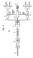
- Figure 4 is a block diagram illustrating an Integrated Services Digital Network receive interface of a channel unit in accordance with the present invention.
- FIG. 2 is a block diagram illustrating a telephone network including an interface between an ILEC and a CLEC in accordance with the present invention.
- the interface portion 60 between the ILEC and the CLEC comprises an ISDN interconnection. In a preferred embodiment, it is a 2 wire basic rate ISDN U-interface (BRI-U).
- BRI-U 2 wire basic rate ISDN U-interface
- the ILEC's central office terminal (COT) 14a and the CLEC's remote terminal (RT) 16a have channel units 26a and 28a, respectively, that each include an ISDN interface 62, rather than the CODEC/hybrid circuit combination of the prior art.
- Figures 1 and 2 omit much of the circuitry in the ILEC's COT and the CLEC's RT that is not relevant to the present invention. This is specifically true of the channel units, where the circuitry not related to the present invention is not shown in the figures.
- the BRI-U protocol is standardized in accordance with ANSI specification T1.601. This standard provides two basic rate (64 Kbps) data channels (termed B channels), and two utility channels.
- the utility channels comprise a 16 Kbps signaling channel, and a 16 Kbps framing/overhead channel that is split between 12 Kbps for framing and 4 Kbps for overhead, for a total of 160 Kbps of which 148 Kbps is for data.
- the channel units include processing capability to remove the robbed bit signaling from the data channels and place it in one of the utility channels. This may be accomplished by a programmed microprocessor, a micro controller, a state machine, combinational logic or any combination of the above.
- bit weights i.e., data sample boundaries
- robbed bit signaling in the CLEC's network and the ILEC's network can be synchronized so that (1) sample boundaries are maintained across the interface and (2) both networks can use the same bit positions for robbed bit signaling such that only one robbed bit appears per every six frames.
- the interface is provided using standard Pulse Code Modulation (PCM) metallic interface circuitry commonly used for U-type (2-wire) digital subscriber line (U-DSL) integrated services digital network (ISDN) line cards of digital switches and by ISDN channel units of digital loop carriers (DLCs).
- PCM Pulse Code Modulation
- U-DSL digital subscriber line
- ISDN integrated services digital network
- DLCs digital loop carriers
- a 2-wire U-ISDN interface provides the necessary performance, however, a 4-wire T-ISDN interface also is possible.
- the CLEC's channel units and the interfacing ILECs channel unit must use the same standard, U or T.
- Figure 3 is a circuit diagram of the transmit portion 62a of an ISDN interface of the present invention generally in accordance with ANSI specification T1.601-1992 entitled "Integrated Services Digital Network (ISDN) - Basic Access Interface for Use on Metallic Loops for Applications on the Network Side of the NT (layer 1 specification)". It should be understood that the interface also would include receive direction circuitry generally in accordance with ANSI specification T1.601-1992 and including complementary modifications to any described below in connection with the transmit direction circuitry.
- Figure 4 is a blobkk diagram of corresponding receive direction circuitry. It also should be understood that the interface between an ILEC and a CLEC typically would comprise multiple copies of the ISDN interface of the present invention in order to provide pathways for a large number of telephone calls to be transferred between the ILEC and the CLEC.
- a standard ISDN transmit interface 62a comprises a plurality of multiplexes 32, 34, 36, 38, 40, 42, 44 for consolidating a plurality of digital signals, such as two voice/data channels and various signaling channels, onto a single tip and ring twisted wire pair. It also includes a cyclic redundancy code generator 48 and associated latch 50 for correcting errors that might occur on the two-wire analog line.
- the output of multiplexer 44 is passed through a scrambler 52 that rearranges the bits of the combined signal to remove repetitive patterns and to reduce correlation between the transmitted and received signals.
- the reduction of correlation between the transmitted and received signals also improves the quality of the hybrid balance circuit (not shown) that is part of a standard ISDN interface and which interconnects the wire pair 60, the ISDN transmit circuit 62a and the ISDN receive circuit (not shown in Figure 3) of the same channel unit.
- the output of scrambler 52 feeds into a 2B1Q encoder 54 which encodes the signal and outputs two separate signals comprising a sign portion and a magnitude portion.
- One final multiplexer 46 consolidates the sign and magnitude signals with a sign and magnitude of a synchronization word generated in a synchronization generator 56.
- the synchronization process is not pertinent to the present invention and therefore is not discussed in detail herein. However, it is a well known aspect of the ISDN framing process.
- Multiplexer 46 is followed by a 2B1Q line interface which further conditions the data and outputs it onto the tip and ring wire pair.
- circuit 62a is in the ILEC's channel unit 14a.
- the inputs of this exemplary ISDN transmission interface would be coupled to the local DLC through the remainder of the CO channel unit 14a.
- wire pair 60 is the wire interface between the ISDN interface circuits of the two facing channel units 14a, 16a.
- multiplexer 34 which, in the ANSI T1.601.2 protocol, has 3 inputs, i.e., two for data/voice channels (termed B channels in ISDN lingo) and one for the signaling channel (termed D channel in ISDN lingo) can be used exactly as intended with the D input used to input signaling information for both data channels.
- the two B inputs of multiplexer 34 can be used to input the two data/voice channels
- the D input can be used to input the signaling corresponding to one of the data channels
- one of the inputs of multiplexer 32 can be used for inputting the signaling information for the other data/voice channel.
- the remaining inputs are unused or can be used for any additional signaling that might be desired.
- the ILEC is likely to use a DLC signaling protocol different from that of the CLEC.
- many, if not most, ILECs utilize Bellcore signaling protocol TR-TSY-000008.
- a CLEC is more likely to utilize the GR-303-CORE signaling protocol.
- the channel units 62 would need to include a function for translating between the two signaling protocols utilized by the ILEC and the CLEC.
- Various designs for an appropriate translation functionality would be readily apparent to persons of ordinary skill in the related arts and could be implemented by a wide variety of means, including, but not limited to, microprocessor, state machine, micro controller, and combinational logic circuitry.
- the receiving channel unit should delay placing the data channel bitstreams received over the interface into its framing structure by an appropriate delay period so that the received data samples correctly fall into the sample slots of the overall framing structure of the receiving network.
- digital loop carriers typically utilize a robbed bit signaling protocol.
- a robbed bit protocol the least significant bit of every sixth frame is "robbed".
- robbed it is meant that the data in that bit position is replaced with a signaling bit which can be used, for instance, for coordinating the equipment at opposite ends of a telephone circuit.
- a signaling bit which can be used, for instance, for coordinating the equipment at opposite ends of a telephone circuit.
- robbed bit signaling reduces the data rate of transmission since 1 out of every 48 (6 x 8) bits cannot contain data. If there are two robbed bits every 6 frames, then the data rate is reduced even further since 2 of every 48 bits is a signaling bit rather than data.
- Digital carrier systems with robbed bit signaling utilize a protocol by which the position of the robbed bit signaling within the framing pattern is determined by the equipment at the remote end. Note that the frames discussed here and below are the frames used by the digital carrier systems within the ILEC and CLEC and not the previously mentioned ISDN frame within which the voice/data, singaling, and maintenance bits are transmitted.
- the channel units are designed to generate and transmit over one of the utility channels data indicative of the frame phasing of the transmitting network. For example, data indicating the start of a frame would be adequate.
- DLCs utilize either a superframe (SF) or extended superframe (ESF) format.
- SF superframe
- ESF extended superframe
- the SF format comprises 12 frame intervals
- the ESF format comprises 24 frame intervals.
- basic frames (a basic frame comprises 24 channels of 8 bit samples plus one framing bit) are 193 bits wide and every sixth basic frame is designated a signaling frame.
- the LSB of each signaling frame is a robbed bit signaling bit.
- the frame phasing information may be transmitted as simply as by changing a continuous stream of zeros in the overhead channel to a short burst of ones at the beginning of the "A" signaling frame of the SF or ESF.
- a circuit for generating and transmitting the frame phasing information may take any form, including, but not limited to, a microprocessor, a micro controller, a state machine, a digital signal processor, combinational logic gates and analog circuitry.
- the facing channel unit can determine (1) the offset between the overall framing structure in its corresponding network and the overall framing structure in the facing network's DLC to maintain sample boundaries and (2) the offset between the signaling bits in its network and the signaling bits of the other network's DLC (ABCD in Figures 3 and 4) so that the robbed bit position for both networks can be matched.
- the offset between corresponding signaling frames (A to A, B to B, etc.) of the facing networks can be anywhere between 0 and 11 frame periods for superframe structure or between 0 and 23 frame periods for extended superframe structure.
- the receiving channel unit should delay the signaling bitstream received over the interface by the determined modulo 6 offset period (2 frames in this example) before inserting the signaling data into the frames of the corresponding network so that the robbed bits inserted by the receiving network will use the same bit positions as the robbed bits of the transmitting network. Thus, there will be only one robbed bit per every six frames.
- One simple solution is to include controllable delay buffers in the receive circuitry of the channel units that is controlled by the offset timing information in order to delay the relevant bitstreams received over the interface by the appropriate duration before inserting that data into the frames of the corresponding network.
- Figure 4 is a block diagram illustrating a receive circuit portion 62b of an ISDN interface 62 in accordance with one preferred embodiment of the invention. It is generally complementary to the transmit circuit portion 62a discussed above and shown in detail in Figure 3 and should be mostly self explanatory to those of skill in the related arts in view of the discussion of Figure 3 above.
- the ISDN signal is received over twisted wire pair 60 from the transmit circuitry 62a of the facing channel unit in 2B1Q encoding.
- a 2B1Q line decoder 70 decodes the signal.
- Descrambler 71 descrambles the bits to place them back in original order.
- Demultiplexer 72 partially demultiplexes the signal received over the ISDN interface into its various channels, including the signaling channels (other than the framing signals) on line 73, the framing signals on line 74, and the data channels on line 75.
- Signaling delay buffer 78 is interposed in path 73 and data delay buffer 76 is interposed in path 75.
- the output of signaling delay buffer 78 is further demultiplexed by demultiplexer 80 into signaling channels 82 and 84 corresponding to each of the signaling channels, respectively.
- the output of data delay buffer 76 is further demultiplexed by demultiplexer 86 into the two distinct data channels 88 and 90, respectively.
- a circuit 92 receives the framing signal from the other network on line 74 as well as the framing signal from its own network on line 94 and determines the frame structure offset between the two networks. Based on the offset information, it generates a signaling delay signal 96 for controlling signaling delay buffer 78 to delay the signaling channel by the appropriate number of frame periods (0 through 5 frames) needed to cause the robbed bit signaling to match up with the robbed bit signaling inserted in the transmitting network. It further generates a data delay signal on line 98 for controlling data delay buffer 76 to delay the data bitstream by the appropriate number of bit periods (0 through 192 bit periods) so that the sample boundaries in the data channels received over the interface are maintained in the receiving network.
- the delay of the robbed bit controllable buffer 78 may be anywhere between 0 and 0.625 milliseconds (i.e., 0 and 5 frame periods).
- the delay period for the data buffer 76 may be anywhere between 0 and 0.125 milliseconds (i.e., 0 and 192 bit periods). This amount of data delay is inconsequential with respect to both data and voice transmissions.
- the robbed bit signaling synchronization feature of the present invention is possible due to the availability of multiple non-data (i.e., maintenance) links in accordance with the ISDN standard circuitry.
- these data links are needed to allow the network to monitor the health of the ISDN terminal at the subscriber location.
- none of that maintenance information is necessary and the signaling and overhead channels can be used as described above. In fact, those channels can be used to transmit any other maintenance information that may be desirable.
- Figure 3 shows the synchronization (framing) signal being input to multiplexer 32.
Landscapes
- Engineering & Computer Science (AREA)
- Computer Networks & Wireless Communication (AREA)
- Physics & Mathematics (AREA)
- Astronomy & Astrophysics (AREA)
- General Physics & Mathematics (AREA)
- Telephonic Communication Services (AREA)
- Interface Circuits In Exchanges (AREA)
- Time-Division Multiplex Systems (AREA)
Abstract
In accordance with the invention, an interface
between an incumbent local exchange carrier's central
office terminal and a competitive local exchange
carrier's remote terminal is provided by an Integrated
Services Digital Network interconnection. Such a
connection provides two basic data channels of 64 Kbps
each and at least one utility channel. The ISDN signal
can be carried over a single wire pair. The interface
may be used to interconnect one or two digital channels.
The channel units may be designed to remove the robbed
bits from the data channels and place them in the
utility channels. Further, the utility channel may be
employed to transmit frame phasing information so that
the networks can synchronize their robbed bit signaling
so that both networks use the same bit positions for
robbed bit signaling thus minimizing data bandwidth
reduction due to robbed bit signaling.
Description
- The invention pertains to an interface between the channel units of an incumbent local exchange carrier and a competitive local exchange carrier. More particularly, the invention pertains to an interface for a competitive local exchange carrier interfacing to an incumbent local exchange carrier's digital subscriber loop under the United States Telecommunications Act of 1996.
- In accordance with the United States Telecommunications Act of 1996, incumbent local exchange carriers (ILECs) that, up to that time, had a monopoly on local telephone service in a given geographic area were required to provide to competitive local exchange carriers (CLECs) access to their connections to subscribers. Accordingly, CLECs could then offer competitive local telephone services to the original ILEC's customers.
- The purpose of the Telecommunications Act of 1996 was to foster competition for local telephone service by assuring that a CLEC could provide services to telephone subscribers with quality comparable to that provided by the ILEC. Accordingly, ILECs need to provide an interface between its central office terminals (COTs) and a CLEC's remote terminal (RT). Despite the name, the CLEC's remote terminal (RT) typically is located in the ILEC's Central Office (CO). The CLEC then typically transports the communication channels via its own network facilities from its RT to its own office where it maintains its own telecommunications equipment, including switching fabric.
- There are three common schemes in use today for interfacing between an ILEC's COT and a CLEC's RT. The first is an analog VF interconnection as illustrated in Figure 1. In short, a
twisted wire pair 12 is provided between the ILEC'sCOT 14 and the CLEC'sRT 16 and the communication data is transmitted between the two terminals in analog form. - At least one goal of the Telecommunications Act of 1996 is to assure that a CLEC can provide the same grade of service (GoS) as the ILEC to telecommunication subscribers. However, many, if not most, ILEC telecommunications networks utilize digital loop carrier (DLC)
systems 18 between their central office terminals, e.g.,COT 14, and remote terminals, e.g.,RT 20, located closer to the subscribers'telephone 22. Typically,remote terminal 20 is located within about two miles of the particular subscriber and the signaling between thecentral office terminal 14 and theremote terminal 20 is digital, termed a digital loop carrier orDLC 18. TheDLC portion 18 is a 4-wire portion comprising twotwisted wire pairs CODEC 24 in the RT interfaces with the subscriber'stelephone equipment 22 and converts the signals between analog and digital. In the U.S., for example, in the digitalloop carrier portion 18 of the network, voice (and data) is sampled at the rate of eight KHz and digitized into eight bit samples, yielding a 64 Kbps (8 KHz times 8 bits) data rate. A digitized voice channel (64 Kbps) is called a DSO. In many if not most digital loop carrier systems, 24 digitized voice channels (DSOs) are time division multiplexed into one signal called a DS1 signal. - When an ILEC provides local area telephone services to its subscribers using digital loop carrier systems between its
RTs 20 andCOTs 14, the signaling between terminals is all digital. However, when a CLEC provides the local area service and interconnects to the ILECs COT via an analog VF interconnection, a digital to analog conversion must be performed in the ILEC's channel unit before the data can be transmitted over the analog interface. Specifically, achannel unit 26 in theCOT 14 must convert signals that are to be transmitted to the CLECRT 16 over theinterface 12 from digital to analog and convert signals received from the CLECRT 16 from analog to digital. - The CLEC's
switching fabric 29 typically is located in the CLEC'scentral office 31 at a remote location from the ILEC'scentral office 27. Accordingly, the CLEC's RT interfaces with the CLEC's Central Office via anotherlink 33, which is commonly a digital carrier link, such as another DLC. Therefore, the CLEC'sRT 16 must convert signals that are to be transmitted to the ILEC'sCOT 16 over theinterface 12 from digital to analog and convert signals received from the ILEC'sCOT 16 from analog to digital. Accordingly, the ILEC'sCOT channel unit 26 and the CLEC'sRT channel unit 28 both containCODECs 25 for converting upstream channels through theinterface 12 from analog to digital and converting downstream channels from digital to analog. - Further, the interface between the ILEC COT 14 and the CLEC
RT 16 is a singletwisted wire pair 12 in which upstream and downstream data are carried on the same wire pair, whereas the digital loop carrier portion of the system is a four wire system with the upstream and downstream signals being transmitted on separate twisted wire pairs. Therefore, eachchannel unit hybrid circuit 23 for converting between 2-wire (the interface side) and 4-wire (the DLC) transmission modes. - Specifically, there are at least three aspects of this link which degrade the service when signals are exchanged between the ILEC and the CLEC. First, there is an increase in background (or quantization) noise. Each time an analog to digital conversion occurs, quantizing noise is introduced because of the finite granularity of the digital code representing each sample of the analog signal. When the ILEC provides service, there is only one analog/digital conversion (at the ILEC's
RT 20 or the ILEC's digital switch). However, when the CLEC provides analog-to-digital service, there are two analog-to-digital conversions namely, at the ILEC's RT and at the CLEC'sRT 16. Accordingly, the background noise when service is provided by a CLEC can be twice that of when service is provided directly by the ILEC. - Secondly, additional noise is introduced by the repeated use of robbed bit signaling (RBS). Robbed bit signaling allows the digital voice or data bit stream to carry signal states necessary for supervision of telephone circuits. A robbed bit is sent in the least significant bit (LSB) position of every 6th voice/data sample. In essence, one out of every 48 bits transmitted is "robbed" for supervisory purposes. When a CLEC provides service, the signals will contain an extra set of robbed bits since the CLEC will add its own robbed bit in its own network while the signal will still contain the robbed bit from the ILEC's network.
- Thirdly, the back to back channel unit configuration used for interconnecting the CLEC and ILEC networks introduces two extra sources of echo. Specifically, when the interconnection between the ILEC and the CLEC is two wire, there must be a hybrid circuit in each channel unit to convert between 2- and 4-wire, thus introducing two more sources of echo in the link. The extra echoes can be avoided by using a 4-wire rather than a 2-wire interface.
- A second option for the interface between the ILEC's COT and the CLEC's RT is a digital cross-connect system (DCS) I/O. A DCS I/O has a plurality, e.g., 24, of DS1 interfaces and a time slot interchange matrix that can be used to cross connect DSO channels. However, a DCS I/O interface is expensive. Further, it provides only DS1 interfaces. Thus, bandwidth is wasted when less than 24 channels are being interconnected.
- Another existing interface is the DS1 interconnection. However, like the DCS I/O solution, this type of interface also has 24 channels and is expensive. Accordingly, bandwidth is wasted when less than 24 channels are being interconnected.
- Accordingly, it is an object of the present invention to provide an improved interface between the channel units of an ILEC and a CLEC.
- In accordance with the invention, an interface between an incumbent local exchange carrier's central office terminal and a competitive local exchange carrier's remote terminal is provided by a modified Integrated Services Digital Network (ISDN) type interconnection. Preferably a modified Basic Rate ISDN U-Interface (BRI-U) in accordance with ANSI standard T1.601 is preferred. Such a connection provides two data clear channels of 64 Kbps each and two utility channels. The utility channels comprise a signaling channel of 16 Kbps and a framing/overhead channel of 16 Kbps (comprising 12 Kbps of ISDN framing structure and 4 Kbps of overhead). The total data rate of the BRI-U is 148 Kbps. The total bit rate is 160 Kbps. The 148 Kbps data signal can be carried over a single wire pair using a 2B1Q line code. The interface may be used to interconnect one or two 64 Kbps channels. The channel units may be designed to remove the robbed bits from the data channels and place them in either the signaling channel or the overhead channel. Also, a superframe (or extended superframe) synchronization signal can be transmitted in the 4 Kbps overhead portion of the framing/overhead channel so that the receiving channel unit can use that information to compensate for offset between its digital carrier frames and the digital carrier frames of the transmitting channel unit. Specifically, (1) the bit weights in the framing structures of the two networks should match so that the data samples are properly designated and (2) the robbed bit signaling should fall in the same bit positions for both networks so as to avoid double robbed bit signaling.
- Figure 1 is a block diagram of a telephone network including an incumbent local exchange carrier and a competitive local exchange carrier in accordance with a prior art scheme.
- Figure 2 is a block diagram of a telephone network including an incumbent local exchange carrier and a competitive local exchange carrier in accordance with the present invention.
- Figure 3 is a circuit diagram illustrating an Integrated Services Digital Network transmit interface of a channel unit in accordance with the present invention.
- Figure 4 is a block diagram illustrating an Integrated Services Digital Network receive interface of a channel unit in accordance with the present invention.
- Figure 2 is a block diagram illustrating a telephone network including an interface between an ILEC and a CLEC in accordance with the present invention. The
interface portion 60 between the ILEC and the CLEC comprises an ISDN interconnection. In a preferred embodiment, it is a 2 wire basic rate ISDN U-interface (BRI-U). In accordance with the invention, the ILEC's central office terminal (COT) 14a and the CLEC's remote terminal (RT) 16a havechannel units ISDN interface 62, rather than the CODEC/hybrid circuit combination of the prior art. It should be understood that, in order not to obfuscate the description, Figures 1 and 2 omit much of the circuitry in the ILEC's COT and the CLEC's RT that is not relevant to the present invention. This is specifically true of the channel units, where the circuitry not related to the present invention is not shown in the figures. - The BRI-U protocol is standardized in accordance with ANSI specification T1.601. This standard provides two basic rate (64 Kbps) data channels (termed B channels), and two utility channels. The utility channels comprise a 16 Kbps signaling channel, and a 16 Kbps framing/overhead channel that is split between 12 Kbps for framing and 4 Kbps for overhead, for a total of 160 Kbps of which 148 Kbps is for data.
- In a preferred embodiment of the invention, the channel units include processing capability to remove the robbed bit signaling from the data channels and place it in one of the utility channels. This may be accomplished by a programmed microprocessor, a micro controller, a state machine, combinational logic or any combination of the above.
- Further, as described fully below, bit weights (i.e., data sample boundaries) as well as robbed bit signaling in the CLEC's network and the ILEC's network can be synchronized so that (1) sample boundaries are maintained across the interface and (2) both networks can use the same bit positions for robbed bit signaling such that only one robbed bit appears per every six frames.
- In accordance with the invention, the interface is provided using standard Pulse Code Modulation (PCM) metallic interface circuitry commonly used for U-type (2-wire) digital subscriber line (U-DSL) integrated services digital network (ISDN) line cards of digital switches and by ISDN channel units of digital loop carriers (DLCs). Accordingly, the interface between the ILEC's channel unit and the CLEC's channel unit is accomplished without introducing extra quantization noise or detectable hybrid echo.
- A 2-wire U-ISDN interface provides the necessary performance, however, a 4-wire T-ISDN interface also is possible. The CLEC's channel units and the interfacing ILECs channel unit, however, must use the same standard, U or T.
- Figure 3 is a circuit diagram of the transmit
portion 62a of an ISDN interface of the present invention generally in accordance with ANSI specification T1.601-1992 entitled "Integrated Services Digital Network (ISDN) - Basic Access Interface for Use on Metallic Loops for Applications on the Network Side of the NT (layer 1 specification)". It should be understood that the interface also would include receive direction circuitry generally in accordance with ANSI specification T1.601-1992 and including complementary modifications to any described below in connection with the transmit direction circuitry. Figure 4 is a blobkk diagram of corresponding receive direction circuitry. It also should be understood that the interface between an ILEC and a CLEC typically would comprise multiple copies of the ISDN interface of the present invention in order to provide pathways for a large number of telephone calls to be transferred between the ILEC and the CLEC. - As shown in Figure 3, a standard ISDN transmit
interface 62a comprises a plurality ofmultiplexes redundancy code generator 48 and associatedlatch 50 for correcting errors that might occur on the two-wire analog line. The output ofmultiplexer 44 is passed through ascrambler 52 that rearranges the bits of the combined signal to remove repetitive patterns and to reduce correlation between the transmitted and received signals. The reduction of correlation between the transmitted and received signals also improves the quality of the hybrid balance circuit (not shown) that is part of a standard ISDN interface and which interconnects thewire pair 60, the ISDN transmitcircuit 62a and the ISDN receive circuit (not shown in Figure 3) of the same channel unit. The output ofscrambler 52 feeds into a2B1Q encoder 54 which encodes the signal and outputs two separate signals comprising a sign portion and a magnitude portion. Onefinal multiplexer 46 consolidates the sign and magnitude signals with a sign and magnitude of a synchronization word generated in asynchronization generator 56. The synchronization process is not pertinent to the present invention and therefore is not discussed in detail herein. However, it is a well known aspect of the ISDN framing process. -
Multiplexer 46 is followed by a 2B1Q line interface which further conditions the data and outputs it onto the tip and ring wire pair. - Let us assume for exemplary purposes that
circuit 62a is in the ILEC'schannel unit 14a. The inputs of this exemplary ISDN transmission interface would be coupled to the local DLC through the remainder of theCO channel unit 14a. At the output,wire pair 60 is the wire interface between the ISDN interface circuits of the two facingchannel units - Since the interface in accordance with a preferred embodiment of the present invention is used to interface two 64 Kbps voice/data channels and their associated signaling information, only 3 or 4 of the input terminals of the first level of multiplexers, i.e., multiplexers 32, 34, 36 and 38, need be used. For instance, in one embodiment of the invention (not specifically illustrated),
multiplexer 34, which, in the ANSI T1.601.2 protocol, has 3 inputs, i.e., two for data/voice channels (termed B channels in ISDN lingo) and one for the signaling channel (termed D channel in ISDN lingo) can be used exactly as intended with the D input used to input signaling information for both data channels. - Alternately, and as expressly illustrated in Figure 3, the two B inputs of
multiplexer 34 can be used to input the two data/voice channels, the D input can be used to input the signaling corresponding to one of the data channels and one of the inputs ofmultiplexer 32 can be used for inputting the signaling information for the other data/voice channel. The remaining inputs are unused or can be used for any additional signaling that might be desired. - As a practical matter, the ILEC is likely to use a DLC signaling protocol different from that of the CLEC. For instance, many, if not most, ILECs utilize Bellcore signaling protocol TR-TSY-000008. However, a CLEC is more likely to utilize the GR-303-CORE signaling protocol. Accordingly, the
channel units 62 would need to include a function for translating between the two signaling protocols utilized by the ILEC and the CLEC. Various designs for an appropriate translation functionality would be readily apparent to persons of ordinary skill in the related arts and could be implemented by a wide variety of means, including, but not limited to, microprocessor, state machine, micro controller, and combinational logic circuitry. - In order to maintain sample boundaries in the data channels transmitted over the interface, information as to the phasing of the frame structure in the network corresponding to the transmitting channel unit must be transmitted over the interface. More specifically, the offset between the overall framing structures of the two facing networks must be determined at the receiving channel unit to maintain the sample boundaries in the data channels transmitted over the interface. The receiving channel unit should delay placing the data channel bitstreams received over the interface into its framing structure by an appropriate delay period so that the received data samples correctly fall into the sample slots of the overall framing structure of the receiving network.
- Additionally, as is well known in the art, digital loop carriers typically utilize a robbed bit signaling protocol. In a robbed bit protocol, the least significant bit of every sixth frame is "robbed". By "robbed" it is meant that the data in that bit position is replaced with a signaling bit which can be used, for instance, for coordinating the equipment at opposite ends of a telephone circuit. With respect to a telephone call carrying voice data, one or even two robbed bits every six frames typically is negligible and will not reduce the quality of the call noticeably. However, with respect to digital data transmissions, robbed bit signaling reduces the data rate of transmission since 1 out of every 48 (6 x 8) bits cannot contain data. If there are two robbed bits every 6 frames, then the data rate is reduced even further since 2 of every 48 bits is a signaling bit rather than data.
- Digital carrier systems with robbed bit signaling utilize a protocol by which the position of the robbed bit signaling within the framing pattern is determined by the equipment at the remote end. Note that the frames discussed here and below are the frames used by the digital carrier systems within the ILEC and CLEC and not the previously mentioned ISDN frame within which the voice/data, singaling, and maintenance bits are transmitted.
- Thus, in addition to synchronizing the sample boundaries of the DLC's of the ILEC and CLEC, it also is desirable to synchronize the robbed bit signaling of the DLCs of the ILEC and CLEC so that any robbed bit signaling of the two DLCs will overlap, i.e., robbed bits inserted by both networks will use the same bit positions. Otherwise, calls that are routed through the CLEC's domain will contain two robbed bits for every six samples rather than one, thus further decreasing data bandwidth.
- Accordingly, in a preferred embodiment of the invention, the channel units are designed to generate and transmit over one of the utility channels data indicative of the frame phasing of the transmitting network. For example, data indicating the start of a frame would be adequate. Typically, DLCs utilize either a superframe (SF) or extended superframe (ESF) format. As is well known in the art, the SF format comprises 12 frame intervals, while the ESF format comprises 24 frame intervals.
- In both formats, basic frames (a basic frame comprises 24 channels of 8 bit samples plus one framing bit) are 193 bits wide and every sixth basic frame is designated a signaling frame. The LSB of each signaling frame is a robbed bit signaling bit.
- The frame phasing information may be transmitted as simply as by changing a continuous stream of zeros in the overhead channel to a short burst of ones at the beginning of the "A" signaling frame of the SF or ESF. A circuit for generating and transmitting the frame phasing information may take any form, including, but not limited to, a microprocessor, a micro controller, a state machine, a digital signal processor, combinational logic gates and analog circuitry.
- With the phasing information transmitted over a utility channel, the facing channel unit can determine (1) the offset between the overall framing structure in its corresponding network and the overall framing structure in the facing network's DLC to maintain sample boundaries and (2) the offset between the signaling bits in its network and the signaling bits of the other network's DLC (ABCD in Figures 3 and 4) so that the robbed bit position for both networks can be matched.
- With respect to robbed bit signaling, the offset between corresponding signaling frames (A to A, B to B, etc.) of the facing networks can be anywhere between 0 and 11 frame periods for superframe structure or between 0 and 23 frame periods for extended superframe structure. However, it is necessary only to keep track of the signaling frame offset by a modulus of 6. Since a robbed bit signal occurs every 6 frames, if the frame offset is, for example, 2, 8, 14 or 20 frames, there will be a robbed bit in the LSB of the 2nd, 8th, 14th, and 20th frames. The receiving channel unit should delay the signaling bitstream received over the interface by the determined modulo 6 offset period (2 frames in this example) before inserting the signaling data into the frames of the corresponding network so that the robbed bits inserted by the receiving network will use the same bit positions as the robbed bits of the transmitting network. Thus, there will be only one robbed bit per every six frames.
- Those of skill in the art will recognize that there are many ways to achieve the necessary delays. One simple solution is to include controllable delay buffers in the receive circuitry of the channel units that is controlled by the offset timing information in order to delay the relevant bitstreams received over the interface by the appropriate duration before inserting that data into the frames of the corresponding network.
- For instance, Figure 4 is a block diagram illustrating a receive
circuit portion 62b of anISDN interface 62 in accordance with one preferred embodiment of the invention. It is generally complementary to the transmitcircuit portion 62a discussed above and shown in detail in Figure 3 and should be mostly self explanatory to those of skill in the related arts in view of the discussion of Figure 3 above. The ISDN signal is received over twistedwire pair 60 from the transmitcircuitry 62a of the facing channel unit in 2B1Q encoding. A2B1Q line decoder 70 decodes the signal.Descrambler 71 descrambles the bits to place them back in original order.Demultiplexer 72 partially demultiplexes the signal received over the ISDN interface into its various channels, including the signaling channels (other than the framing signals) online 73, the framing signals online 74, and the data channels online 75. Signalingdelay buffer 78 is interposed inpath 73 and data delaybuffer 76 is interposed inpath 75. The output of signalingdelay buffer 78 is further demultiplexed bydemultiplexer 80 into signalingchannels buffer 76 is further demultiplexed bydemultiplexer 86 into the twodistinct data channels - A
circuit 92 receives the framing signal from the other network online 74 as well as the framing signal from its own network online 94 and determines the frame structure offset between the two networks. Based on the offset information, it generates asignaling delay signal 96 for controllingsignaling delay buffer 78 to delay the signaling channel by the appropriate number of frame periods (0 through 5 frames) needed to cause the robbed bit signaling to match up with the robbed bit signaling inserted in the transmitting network. It further generates a data delay signal online 98 for controlling data delaybuffer 76 to delay the data bitstream by the appropriate number of bit periods (0 through 192 bit periods) so that the sample boundaries in the data channels received over the interface are maintained in the receiving network. - In accordance with this aspect of the invention, the delay of the robbed bit
controllable buffer 78 may be anywhere between 0 and 0.625 milliseconds (i.e., 0 and 5 frame periods). The delay period for thedata buffer 76 may be anywhere between 0 and 0.125 milliseconds (i.e., 0 and 192 bit periods). This amount of data delay is inconsequential with respect to both data and voice transmissions. - Note that, if the robbed bit signaling offset is 0, 6, 12 or 18, the incoming signaling frame matches the outgoing, although the impact of a change of state of A, B, C and D signaling bits is delayed unless the offset is 0. Such a delay is of little consequence compared with the benefit of avoiding robbing an additional bit.
- The robbed bit signaling synchronization feature of the present invention is possible due to the availability of multiple non-data (i.e., maintenance) links in accordance with the ISDN standard circuitry. In typical ISDN applications, these data links are needed to allow the network to monitor the health of the ISDN terminal at the subscriber location. However, for the present application, none of that maintenance information is necessary and the signaling and overhead channels can be used as described above. In fact, those channels can be used to transmit any other maintenance information that may be desirable. Figure 3, for example, shows the synchronization (framing) signal being input to
multiplexer 32. - Having thus described a few particular embodiments of the invention, various alterations, modifications, and improvements will readily occur to those skilled in the art.
- Accordingly, the foregoing description is by way of example only, and not limiting. For instance, an embodiment of the invention using a T-type ISDN interface would adhere to the construct disclosed in ANSI specification T1.605. The invention is limited only as defined in the following claims.
Claims (40)
- A circuit for interfacing between a digital loop carrier that forms at least a portion of a first telephone network interconnecting a plurality of subscribers for providing communications service to said subscribers and a second telephone network for providing alternate communications service to said subscribers, said circuit for interfacing comprising an integrated services digital network interface.
- The circuit set forth in claim 1 wherein said integrated services digital network interface comprises a first channel unit corresponding to said first network and a second channel unit corresponding to said second network.
- The circuit set forth in claim 1 wherein said interface is a U-type integrated services digital network interface.
- The circuit set forth in claim 1 wherein said circuit comprises two facing integrated services digital network interfaces.
- The circuit set forth in claim 1 wherein said integrated services digital network interface comprises a Basic Rate integrated services digital network interface.
- The circuit set forth in claim 5 wherein said integrated services digital network interface comprises a Basic Rate integrated services digital network interface in accordance with ANSI specification T1.601-1992.
- The circuit set forth in claim 1 wherein said interface is a T-type integrated services digital network interface.
- The circuit set forth in claim 2 wherein said integrated services digital network interface comprises a first data channel, a second data channel, and a utility channel and wherein communications data is transported between said first network and said second network over said data channels, said integrated services digital network interface further comprising a first circuit in at least one of said channel units for generating a signal indicative of frame phasing in said network corresponding to said channel unit and placing said frame phasing information on said utility channel.
- The circuit set forth in claim 8 wherein each of said first and second channel units includes said first circuit.
- The circuit set forth in claim 9 wherein said frame phasing signal indicates the start of a transmission frame.
- The circuit set forth in claim 10 further comprising a second circuit in at least the other of said channel units for receiving said frame phase signal and delaying signals received over said data channels of said interface such that robbed bit signaling in said first and second networks overlap with respect to data transferred over said interface.
- The circuit set forth in claim 11 wherein:said first and second networks have first and second framing structures, respectively;said robbed bit signaling information is transmitted over said interface in said signaling channel; andsaid second circuit delays said signaling channel such that robbed bit signaling in said first and second networks overlap with respect to data transferred over said interface and delays said data channels such that bits of said communications data transmitted over said interface are assigned the same bit weight in said first and second framing structures.
- The circuit set forth in claim 12 wherein each of said first and second channel units includes said second circuit.
- The circuit set forth in claim 13 wherein said second circuit comprises a programmable delay buffer.
- The circuit set forth in claim 1 wherein said integrated services digital network interface uses a 2B1Q line code.
- An interface between a digital loop carrier that forms at least a portion of a first telephone network interconnecting a plurality of subscribers for providing communications service to said subscribers and a second telephone network for providing alternate communications service to said subscribers, said interface comprising:a first channel unit associated with said first network comprising an integrated services digital network interface;a second channel unit associated with said second network comprising an integrated services digital network interface; anda wire pair interconnecting said first and second integrated services digital network interfaces.
- The circuit set forth in claim 16 wherein said interface is a U-type integrated services digital network interface.
- The circuit set forth in claim 16 wherein said interface is a T-type integrated services digital network interface and said wire pair comprises two wire pairs.
- The circuit set forth in claim 16 wherein said integrated services digital network interface comprises a Basic Rate integrated services digital network interface.
- The circuit set forth in claim 19 wherein said integrated services digital network interface comprises a Basic Rate integrated services digital network interface in accordance with ANSI specification T1.601-1992.
- The circuit set forth in claim 16 wherein said integrated services digital network interface comprises a first data channel, a second data channel, and a utility channel and wherein communications data is transported between said first network and said second network over said data channels, said integrated services digital network interface further comprising a first circuit in at least one of said channel units for generating a signal indicative of frame phasing in said network corresponding to said channel unit and placing said frame phasing information on said utility channel.
- The circuit set forth in claim 21 wherein each of said first and second channel units includes said first circuit.
- The circuit set forth in claim 22 wherein said frame phasing signal indicates a start of a transmission frame.
- The circuit set forth in claim 23 further comprising a second circuit in at least the other of said channel units for receiving said frame phase signal and delaying data received over said data channels of said interface such that robbed bit signaling in said first and second networks overlap with respect to data transferred over said interface.
- The circuit set forth in claim 24 wherein:said first and second networks have first and second framing structures, respectively;said robbed bit signaling information is transmitted over said interface in said signaling channel; andsaid second circuit delays said signaling channel such that robbed bit signaling in said first and second networks overlap with respect to data transferred over said interface and delays said data channels such that bits of said communications data transmitted over said interface are assigned the same bit weight in said first and second framing structures.
- The circuit set forth in claim 25 wherein each of said first and second channel units includes said second circuit.
- The circuit set forth in claim 26 wherein said second circuit comprises a programmable delay buffer.
- The circuit set forth in claim 16 wherein said integrated services digital network interface uses a 2B1Q line code.
- The circuit set forth in claim 16 wherein said second telephone network comprises a second digital loop carrier coupled to said second channel unit.
- A method of interconnecting a first telephone network of a competitive local exchange carrier to a second telephone network of an incumbent local exchange carrier that interconnects a plurality of subscribers, said second telephone network comprising a digital subscriber loop, said method comprising the step of:
transporting telephone calls between said first and second telephone networks using an integrated services digital network interface. - The method set forth in claim 30 wherein said step comprises using a U-type integrated services digital network interface.
- The method set forth in claim 30 wherein said step comprises using first and second facing integrated services digital network interfaces corresponding to said first and second networks, respectively.
- The method set forth in claim 30 wherein said step comprises using a Basic Rate integrated services digital network interface.
- The method set forth in claim 33 wherein said step comprises using a Basic Rate integrated services digital network interface in accordance with ANSI specification T1.601-1992.
- The method set forth in claim 32 wherein said step comprises using a T-type integrated services digital network interface.
- The method set forth in claim 34 further comprising the step of:
transporting between said first and second networks a signal indicative of frame phasing in a transmitting one of said networks. - The circuit set forth in claim 36 wherein said frame phasing signal indicates a start of a frame.
- The circuit set forth in claim 37 further comprising the steps of:receiving said frame phasing signal in a receiving one of said networks;delaying data received over said interface such that robbed bit signaling in said first and second networks overlap with respect to data transported over said interface and such that bits of data of said telephone calls transmitted over said interface are assigned the same bit weight in said first and second networks.
- The circuit set forth in claim 37 wherein said interface comprises two data channels for transporting said data and at least one utility channel, said method further comprising the step of:
generating a signal indicative of the location of robbed bit signaling in said transmitted frame and transporting said signal over said utility channel. - The method set forth in claim 30 further comprising the step of:
using a 2B1Q line code over said interface.
Applications Claiming Priority (2)
| Application Number | Priority Date | Filing Date | Title |
|---|---|---|---|
| US454930 | 1999-12-03 | ||
| US09/454,930 US6788678B1 (en) | 1999-12-03 | 1999-12-03 | Interface between channel units of multiple local exchange carriers |
Publications (1)
| Publication Number | Publication Date |
|---|---|
| EP1107616A2 true EP1107616A2 (en) | 2001-06-13 |
Family
ID=23806656
Family Applications (1)
| Application Number | Title | Priority Date | Filing Date |
|---|---|---|---|
| EP00310502A Withdrawn EP1107616A2 (en) | 1999-12-03 | 2000-11-27 | Improved interface between channel units of multiple local exchange carriers |
Country Status (4)
| Country | Link |
|---|---|
| US (1) | US6788678B1 (en) |
| EP (1) | EP1107616A2 (en) |
| CN (1) | CN1299206A (en) |
| CA (1) | CA2326617A1 (en) |
Families Citing this family (1)
| Publication number | Priority date | Publication date | Assignee | Title |
|---|---|---|---|---|
| US7187712B2 (en) * | 2001-04-02 | 2007-03-06 | Texas Instruments Incorporated | Efficient framing of overhead channel for ADSL modems |
Family Cites Families (8)
| Publication number | Priority date | Publication date | Assignee | Title |
|---|---|---|---|---|
| US5519719A (en) * | 1991-12-19 | 1996-05-21 | Adc Telecommunications, Inc. | Universal pattern generator |
| US5305312A (en) * | 1992-02-07 | 1994-04-19 | At&T Bell Laboratories | Apparatus for interfacing analog telephones and digital data terminals to an ISDN line |
| US5774530A (en) * | 1996-02-09 | 1998-06-30 | Bell Atlantic Network Services, Inc. | Telecommunications network circuit usage measurement |
| US5875229A (en) * | 1996-10-15 | 1999-02-23 | Motorola Inc. | System and device for, and method of, detecting, characterizing, and mitigating deterministic distortion in a communications network |
| US5940403A (en) * | 1996-11-07 | 1999-08-17 | Adtran, Inc. | Quarter-rate 2B1Q ISDN architecture with embedded differential delay compensation for extending range of DDS communications |
| US5896390A (en) * | 1997-02-21 | 1999-04-20 | Adtran, Inc. | Two wire, sub-rate 2B1Q ISDN architecture |
| US6104730A (en) * | 1997-11-25 | 2000-08-15 | International Business Machines Corporation | System, method and article of manufacture for high bit rate access over robbed bit trunks |
| US6445698B1 (en) * | 1998-09-08 | 2002-09-03 | Hyperedge Corporation | Two wire DDS transport system |
-
1999
- 1999-12-03 US US09/454,930 patent/US6788678B1/en not_active Expired - Lifetime
-
2000
- 2000-11-23 CA CA002326617A patent/CA2326617A1/en not_active Abandoned
- 2000-11-27 EP EP00310502A patent/EP1107616A2/en not_active Withdrawn
- 2000-12-01 CN CN00134470A patent/CN1299206A/en active Pending
Also Published As
| Publication number | Publication date |
|---|---|
| CA2326617A1 (en) | 2001-06-03 |
| US6788678B1 (en) | 2004-09-07 |
| CN1299206A (en) | 2001-06-13 |
Similar Documents
| Publication | Publication Date | Title |
|---|---|---|
| US5610922A (en) | Voice plus 4-wire DDS multiplexer | |
| US5668814A (en) | Dual DDS data multiplexer | |
| US5398249A (en) | System for providing simultaneous multiple circuit-switched type communications on an ISDN basic rate interface | |
| US6879603B1 (en) | Processor-based voice and data time slot interchange system | |
| US5060227A (en) | Digital telephone switch with simultaneous dual PCM format compatibility | |
| US5555260A (en) | Decentralized base station for reducing bandwidth requirements for communications to and from radio transmitter-receivers in a telecommunications network | |
| US5115431A (en) | Method and apparatus for packet communications signaling | |
| US5452306A (en) | Out-of-band embedded overhead architecture for a transmission network | |
| US5625685A (en) | Network termination unit | |
| AU687073B2 (en) | Added bit signalling in a telecommunications system | |
| WO1996029793A9 (en) | Multiple digital signal multiplexer | |
| US6781985B1 (en) | Time-division multiplexer | |
| WO2000076099A9 (en) | Sub-rate out-of-band tdm signaling channel | |
| US6487222B1 (en) | Quarter-rate 2B1Q ISDN architecture with embedded differential delay compensation for extending range of DDS communications | |
| US5446731A (en) | Signaling channel data transmitting/receiving circuit of a primary multiplexer | |
| IE65860B1 (en) | Automatic telecommunications systems | |
| US5436895A (en) | Subscriber transmission system | |
| US6788678B1 (en) | Interface between channel units of multiple local exchange carriers | |
| US5712898A (en) | D4 channel bank with multi-mode formatted, performance-monitoring communication bus | |
| US6519267B1 (en) | Use of robbed framing bits to provide secondary pots channel over extended range ISDN communications network | |
| GB2072464A (en) | Line supplied telephone interface | |
| NZ251727A (en) | Transmitting ancillary information in time division multiplex system | |
| US6744751B1 (en) | System for transporting full T1 frame of data/voice channels and additional DSO data channels over E1 communication link | |
| US7366198B2 (en) | Method and system for packet and circuit telephony in a distributed telecommunications switching system | |
| KR100270442B1 (en) | A transceiver for selecting a channel to connect isdn |
Legal Events
| Date | Code | Title | Description |
|---|---|---|---|
| PUAI | Public reference made under article 153(3) epc to a published international application that has entered the european phase |
Free format text: ORIGINAL CODE: 0009012 |
|
| AK | Designated contracting states |
Kind code of ref document: A2 Designated state(s): AT BE CH CY DE DK ES FI FR GB GR IE IT LI LU MC NL PT SE TR |
|
| AX | Request for extension of the european patent |
Free format text: AL;LT;LV;MK;RO;SI |
|
| STAA | Information on the status of an ep patent application or granted ep patent |
Free format text: STATUS: THE APPLICATION HAS BEEN WITHDRAWN |
|
| 18W | Application withdrawn |
Effective date: 20030509 |