EP1107487A1 - Optical link for the transmission of a RF signal eliminating distortions - Google Patents
Optical link for the transmission of a RF signal eliminating distortions Download PDFInfo
- Publication number
- EP1107487A1 EP1107487A1 EP00310524A EP00310524A EP1107487A1 EP 1107487 A1 EP1107487 A1 EP 1107487A1 EP 00310524 A EP00310524 A EP 00310524A EP 00310524 A EP00310524 A EP 00310524A EP 1107487 A1 EP1107487 A1 EP 1107487A1
- Authority
- EP
- European Patent Office
- Prior art keywords
- optical
- signals
- signal
- modulated
- fiber
- Prior art date
- Legal status (The legal status is an assumption and is not a legal conclusion. Google has not performed a legal analysis and makes no representation as to the accuracy of the status listed.)
- Withdrawn
Links
Images


Classifications
-
- H—ELECTRICITY
- H04—ELECTRIC COMMUNICATION TECHNIQUE
- H04B—TRANSMISSION
- H04B10/00—Transmission systems employing electromagnetic waves other than radio-waves, e.g. infrared, visible or ultraviolet light, or employing corpuscular radiation, e.g. quantum communication
- H04B10/25—Arrangements specific to fibre transmission
- H04B10/2575—Radio-over-fibre, e.g. radio frequency signal modulated onto an optical carrier
-
- H—ELECTRICITY
- H04—ELECTRIC COMMUNICATION TECHNIQUE
- H04B—TRANSMISSION
- H04B10/00—Transmission systems employing electromagnetic waves other than radio-waves, e.g. infrared, visible or ultraviolet light, or employing corpuscular radiation, e.g. quantum communication
- H04B10/25—Arrangements specific to fibre transmission
- H04B10/2507—Arrangements specific to fibre transmission for the reduction or elimination of distortion or dispersion
Definitions
- the present invention relates generally to high performance optical links and, more particularly, to an optical link that utilizes optical carriers transmitted using a single transmission medium such as an optical fiber in a way which substantially eliminates unwanted distortion signals accumulated during the transmission process.
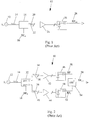
- FIG. 1 illustrates one such example.
- An optical link generally indicated by the reference number 10, shown in FIG. 1 utilizes an optical light source 12 of a selected wavelength ⁇ 1 , to produce an optical carrier 14. The specific wavelength was chosen to fall within one of the transmissive windows in the typical optical fiber absorption spectrum.
- An RF signal 16 is modulated onto the optical carrier 14 using a modulator 18.
- a modulated optical signal 20 is then directed into an optical fiber 22.
- Optical devices, such as an optical amplifier 24, may be spliced into optical fiber 22. Modulated optical signal 20 is received at the other end of optical fiber 22 by a receiver 26, and, thereafter, the RF signal is regenerated as an RF out signal 28.
- this dual fiber optical link is generally indicated by the reference number 30.
- single laser source 12 is used and single optical carrier 14 is directed into a modulator 32.
- optical carrier 14 is split into first and second optical signals 34 and 36 after RF modulation signal 18 is encoded thereon.
- Modulator 32 is designed such that RF modulation 18 on first optical signal 34 and RF modulation 18 on second optical signal 36 emitted at the output ports 1 and 2, respectively, have a predetermined relationship.
- the RF modulation on first optical signal 34 and the RF modulation on second optical signal 36 can be manipulated to be 180° out of phase at the two output ports of modulator 32.
- optical signals 34 and 36 at the output ports 1 and 2, respectively, are of the same wavelength while the RF modulation on first optical signal 34 is the exact reciprocal of the RF modulation on second optical signal 36. Therefore, unless optical signals 34 and 36 are transmitted on two separate optical fibers 38 and 40, the RF modulation on optical signals 34 and 36, being exactly out of phase, will cancel out and the encoded information will be lost.
- the RF modulation signals are recovered from optical signals 34 and 36 by separate detectors 46 and 48, respectively.
- the CSO on each of the two recovered RF signals is in phase with respect to one another since the noise was accumulated during the transmission process, while the RF signals themselves are 180° out of phase, as dictated by the characteristics of modulator 32.
- Recovered RF signals 50 and 52 are combined using a 180° combiner, in which one of the recovered RF signals, as affected by the noise accumulation, is sent through a 180° phase compensator (not shown) then added to the other recovered RF signal, also as affected by the noise accumulation, such that the CSO on the two recovered RF modulation signals is now 180° out of phase so as to substantially cancel when added. Furthermore, the recovered RF signals themselves are in phase as a result of the 180° phase compensator. Thus, the total RF signal at the destination is increased by a factor of two as compared to single wavelength, single fiber optical link 10. As a result, the CNR of dual fiber optical link 30 improves by 3dB.
- dual fiber optical link 30 has a drawback in that two separate optical fibers 38 and 40 are required for the transmission of each data set. Two fibers may not be available for use between all data sources and receivers, and this fact will add to the infrastructure cost of using the dual fiber approach. With regard to proper operation of dual fiber optical link 30, a further problem is posed in the system architecture because in this case two matching sets of optical components are necessary between the data source and the destination. Such matching sets of optical fibers, optical amplifiers, and receivers may simply be unavailable. Moreover, the cost of building an optical communication infrastructure using this two fiber optical link is nearly twice as the cost of a single wavelength, single fiber optical link.
- the present invention utilizes a highly advantageous and heretofore unseen optical link configuration and associated method using a single transmission medium which overcomes the foregoing limitations and disadvantages while still improving the CSO and CNR performance of the optical link.
- the optical link includes means for transmitting first and second optical signals through the optical fiber.
- the optical signals have been modulated with the RF signal in such a way that a predetermined relationship is produced between the RF signals modulated on the first and second optical signals.
- the opposing end of the optical fiber is equipped with an arrangement for receiving the modulated first and second optical signals, including the unwanted distortion signals produced during transmission through the optical fiber, and for regenerating the RF signal from the modulated first and second optical signals while causing the unwanted distortion signals to be canceled based on the predetermined relationship.
- FIG. 1 is a block diagram of a prior art optical link which uses one light source of a single wavelength, one optical fiber as the transmission medium and one receiver for the detection and decoding of the RF signal.
- FIG. 2 is a block diagram of another prior art optical link which uses a dual fiber method to transmit the RF signal on two optical carriers through two optical fibers. Upon detection at two receivers, the received signals are added in such a way that the RF signal is regenerated while the unwanted distortion signals accumulated during transmission through the optical fibers are canceled.
- FIG. 3 is a block diagram of a high performance optical link manufactured in accordance with the present invention shown here to illustrate an embodiment using optical carriers of two wavelengths, a wavelenthg-division multiplexer and a wavelength-division demultiplexer.
- FIG. 4 is a block diagram of an alternative high performance optical link also manufactured in accordance with the present invention shown here to illustrate an embodiment using a time-division multiplexer and a time-division demultiplexer.
- FIG. 3 illustrates one implementation of a high performance optical link, generally indicated by the reference number 60 and manufactured in accordance with the present invention.
- Optical link 60 includes two optical light sources 62 and 64, which emit first and second optical carriers 66 and 68 at first and second optical wavelengths ⁇ 1 , and ⁇ 2 , respectively.
- First and second optical carriers 66 and 68 are combined using a combiner 70, and directed to the input port of a Mach-Zender (MZ) modulator 74.
- RF signal 75 on which the original information to be transmitted is encoded, is modulated onto combined optical carrier 72 at MZ modulator 74 such that first and second optical signals 76 and 78 are produced at the output ports 1 and 2 of MZ modulator 74.
- First and second optical signals 76 and 78 each contain both first and second optical carriers 66 and 68 with optical wavelengths ⁇ 1 , and ⁇ 2 .
- First and second optical signals 76 and 78 are modulated by the same RF signal 75, however, MZ modulator 74 is designed to produce a phase difference of 180° between the RF signal modulated onto first optical signal 76 and the RF signal modulated onto second optical signal 78.
- the RF signal modulated onto first optical signal 76 is the exact complement of the RF signal modulated onto second optical signal 78.
- the phase of the RF signal modulated onto first optical signal 76 is indicated as [A]
- the phase of the RF signal modulated onto second optical signal 78 is indicated as [B].
- Optical signals 76 and 78 at the MZ modulator output ports are marked with wavelength indications ⁇ 1 , and ⁇ 2 to signify that both of these optical wavelengths are present at each MZ modulator output port.
- first and second optical signals 76 and 78 are directed into first and second input channels 80 and 82, respectively, of a wavelength division multiplexer (WDM) 84.
- WDM 84 is designed to select first optical carrier 66, with optical wavelength ⁇ 1 , and phase [A], from first optical signal 76 at first input channel 80 and to select second optical carrier 68, with optical wavelength ⁇ 2 and phase [B], from second optical signal 78 at second input channel 82. Then WDM 84 combines the selected optical signals 76 and 78 into a multiplexed signal 86 and transmits multiplexed signal 86 at an output channel 87.
- multiplexed signal 86 contains first optical carrier 66, with optical wavelength ⁇ 1 , and phase [A], and second optical carrier 68, with optical wavelength ⁇ 2 and phase [B].
- First and second optical carriers 66 and 68 have the same RF signal modulated thereon but with a phase difference of 180° between the RF signals on the two optical carriers.
- Multiplexed signal 86 from output channel 87 of WDM 84 is directed into a single optical fiber 88. Unwanted distortion signals are accumulated on the multiplexed signal during transmission through optical fiber 88. As in prior art optical links 10 and 30, additional optical devices, such as optical amplifiers (not shown), may be inserted into optical fiber 88. However, it should be noted that, from output channel 87 of WDM 84 to a demultiplexing WDM 90 to be described hereinafter, only a single continuous transmission medium is required, unlike the prior art shown in FIG. 2.
- multiplexed signal 86 is directed into an input channel 89 of a demultiplexing WDM 90.
- Demultiplexing WDM 90 separates multiplexed signal 86 into a first optical carrier 91, with optical wavelength ⁇ 1 , and phase [A], and a second optical carrier 92, with optical wavelength ⁇ 2 and phase [B].
- Separated optical carriers 91 and 92 exit from demultiplexing WDM 90 at first and second output channels 93 and 94, and are then directed to first and second receivers 96 and 98, respectively.
- RF signals 100 and 102, including the unwanted distortion signals, modulated on the separated first and second optical carriers 91 and 92 are recovered by first and second receivers 96 and 98, respectively.
- Recovered RF signals 100 and 102 are then recombined using a 180° combiner 106 in which the phase of one of the recovered RF signals, including the unwanted distortion signals, is shifted by 180° and the resulting phase shifted RF signal is added to the other, unshifted RF signal.
- the unwanted distortion signals accumulated on the phase shifted and unshifted RF signals then become 180° out of phase and thus cancel when added.
- the RF signals with the original information encoded thereon are brought back in phase by a 180° combiner 106, thus the original RF signal is regenerated.
- the CNR improves by 3 dB compared to the prior art shown in FIG. 1, and the CSO improvement will be between 6 and 12 dB.
- the technique of the present invention can be achieved in other configurations such as, for example, one which uses a single light source and one transmission medium while incorporating the unwanted distortion signal cancellation scheme.
- Such an example is illustrated in FIG. 4, and the configuration is generally referred to by the reference number 130.
- a single light source 132 emits an optical carrier 134 with wavelength ⁇ 1 , which is directed into a modulator/splitter 136.
- An RF signal 138 is modulated onto optical carrier 134, which is then split into two optical signals 140 and 142 with a 180° phase difference produced between optical signals 140 and 142 at the modulator output Ports 1 and 2.
- Optical signals 140 and 142 on which RF signal 138 have been modulated with phase [A] and phase [B], respectively, are then directed into a time-division multiplexer (TDM) 148 which splits optical signals 140 and 142 into smaller information packets that are sent out of a TDM output port 150 in an alternating, sequential manner as a time-multiplexed signal 152, as shown schematically in FIG. 4, through a single optical fiber 154.
- TDM time-division multiplexer
- optical devices such as an optical amplifier 156 may be spliced into optical fiber 154.
- time-multiplexed signal 152 is received at the opposing end of optical fiber 154 by a demultiplexing TDM 160 which reconstructs optical signals 140 and 142 from the received time-multiplexed signal 152.
- the RF signals including the unwanted distortion signals are recovered from optical signals 140 and 142 using first and second receivers 162 and 164, respectively.
- the resulting RF signals 166 and 168 are added using a 180° combiner 170.
- the unwanted distortion signals then become 180° out of phase and thus cancel when added.
- the RF signals are brought back into phase by the 180° combiner, resulting in regeneration of the original RF signal.
- the CNR improves by 3 dB compared to the prior art shown in FIG. 1, and the CSO improvement will be between 6 and 12 dB.
- optical link and associated method disclosed herein may be provided in a variety of different configurations and the method may be practiced in a variety of ways, it should be understood that the present invention may be embodied in many other specific ways without departing from the spirit or scope of the invention. Therefore, the present examples and methods are to be considered as illustrative and not restrictive, and the invention is not to be limited to the details given herein, but may be modified within the scope of the appended claims.
Landscapes
- Physics & Mathematics (AREA)
- Electromagnetism (AREA)
- Engineering & Computer Science (AREA)
- Computer Networks & Wireless Communication (AREA)
- Signal Processing (AREA)
- Optical Communication System (AREA)
Abstract
Description
- The present invention relates generally to high performance optical links and, more particularly, to an optical link that utilizes optical carriers transmitted using a single transmission medium such as an optical fiber in a way which substantially eliminates unwanted distortion signals accumulated during the transmission process.
- Optical links early in the development of communication systems using a light transmission medium such as, for example, an optical fiber were based on a single optical carrier of a specific wavelength. FIG. 1 illustrates one such example. An optical link, generally indicated by the
reference number 10, shown in FIG. 1 utilizes anoptical light source 12 of a selected wavelength λ1, to produce anoptical carrier 14. The specific wavelength was chosen to fall within one of the transmissive windows in the typical optical fiber absorption spectrum. AnRF signal 16 is modulated onto theoptical carrier 14 using amodulator 18. A modulatedoptical signal 20 is then directed into anoptical fiber 22. Optical devices, such as anoptical amplifier 24, may be spliced intooptical fiber 22. Modulatedoptical signal 20 is received at the other end ofoptical fiber 22 by areceiver 26, and, thereafter, the RF signal is regenerated as an RFout signal 28. - While prior art
optical link 10 is generally suited to its intended purpose, a number of disadvantages have been discovered. The main disadvantages of the single wavelength, single fiber optical link are its relatively limited data capacity and significant data signal degradation. This degradation is due at least in part to optical carrier intensity attenuation and/or composite second order (CSO) noise accumulation during transmission through the optical fiber. - One prior art approach in an attempt to improve data transfer uses multiple optical carriers. However, in an optical link, the number of distinct sets of data which can be transmitted through a single optical fiber on multiple optical carriers is limited by the fact that, if portions of the RF signals modulated onto the optical carriers overlap, those portions will cancel each other and result in crosstalk, or significant reductions in the data fidelity. Hence, only a limited number of distinct data can be transmitted using this optical link scheme. Moreover, when optical amplifiers are inserted into the transmission medium in an attempt to alleviate the attenuation problem, the accumulated noise is amplified along with the optical carrier. For this reason, the carrier-to-noise (CNR) ratio is not improved with the addition of optical amplifiers in a single wavelength, single fiber optical link or in a multiple wavelength, single fiber optical link.
- Another prior art attempt in resolving the foregoing problems has been to use a modulator having dual outputs directed into two optical fibers. Now referring to FIG. 2, this dual fiber optical link is generally indicated by the
reference number 30. In this dual fiberoptical link 30, as in previously described single wavelength, single fiberoptical link 10,single laser source 12 is used and singleoptical carrier 14 is directed into amodulator 32. However,optical carrier 14 is split into first and secondoptical signals RF modulation signal 18 is encoded thereon.Modulator 32 is designed such thatRF modulation 18 on firstoptical signal 34 andRF modulation 18 on secondoptical signal 36 emitted at theoutput ports optical signal 34 and the RF modulation on secondoptical signal 36 can be manipulated to be 180° out of phase at the two output ports ofmodulator 32. Note thatoptical signals output ports optical signal 34 is the exact reciprocal of the RF modulation on secondoptical signal 36. Therefore, unlessoptical signals optical fibers optical signals - Still discussing dual fiber
optical link 30 shown in FIG. 2, at the receiving end ofoptical fibers optical signals separate detectors modulator 32. RecoveredRF signals optical link 10. As a result, the CNR of dual fiberoptical link 30 improves by 3dB. - Although the CSO problem has been reduced, abovementioned dual fiber
optical link 30 has a drawback in that two separateoptical fibers optical link 30, a further problem is posed in the system architecture because in this case two matching sets of optical components are necessary between the data source and the destination. Such matching sets of optical fibers, optical amplifiers, and receivers may simply be unavailable. Moreover, the cost of building an optical communication infrastructure using this two fiber optical link is nearly twice as the cost of a single wavelength, single fiber optical link. - The present invention utilizes a highly advantageous and heretofore unseen optical link configuration and associated method using a single transmission medium which overcomes the foregoing limitations and disadvantages while still improving the CSO and CNR performance of the optical link.
- As will be described in more detail hereinafter, there is disclosed herein a high performance optical link and associated method for transmission of an RF signal using a single transmission medium, such as an optical fiber having opposing ends and configured such that unwanted distortion signals are produced when optical signals pass through the optical fiber. At one end of the optical fiber, the optical link includes means for transmitting first and second optical signals through the optical fiber. The optical signals have been modulated with the RF signal in such a way that a predetermined relationship is produced between the RF signals modulated on the first and second optical signals. The opposing end of the optical fiber is equipped with an arrangement for receiving the modulated first and second optical signals, including the unwanted distortion signals produced during transmission through the optical fiber, and for regenerating the RF signal from the modulated first and second optical signals while causing the unwanted distortion signals to be canceled based on the predetermined relationship.
- FIG. 1 is a block diagram of a prior art optical link which uses one light source of a single wavelength, one optical fiber as the transmission medium and one receiver for the detection and decoding of the RF signal.
- FIG. 2 is a block diagram of another prior art optical link which uses a dual fiber method to transmit the RF signal on two optical carriers through two optical fibers. Upon detection at two receivers, the received signals are added in such a way that the RF signal is regenerated while the unwanted distortion signals accumulated during transmission through the optical fibers are canceled.
- FIG. 3 is a block diagram of a high performance optical link manufactured in accordance with the present invention shown here to illustrate an embodiment using optical carriers of two wavelengths, a wavelenthg-division multiplexer and a wavelength-division demultiplexer.
- FIG. 4 is a block diagram of an alternative high performance optical link also manufactured in accordance with the present invention shown here to illustrate an embodiment using a time-division multiplexer and a time-division demultiplexer.
- Attention is now directed to FIG. 3, which illustrates one implementation of a high performance optical link, generally indicated by the
reference number 60 and manufactured in accordance with the present invention.Optical link 60 includes twooptical light sources optical carriers optical carriers combiner 70, and directed to the input port of a Mach-Zender (MZ)modulator 74.RF signal 75, on which the original information to be transmitted is encoded, is modulated onto combinedoptical carrier 72 atMZ modulator 74 such that first and secondoptical signals output ports MZ modulator 74. First and secondoptical signals optical carriers - First and second
optical signals same RF signal 75, however,MZ modulator 74 is designed to produce a phase difference of 180° between the RF signal modulated onto firstoptical signal 76 and the RF signal modulated onto secondoptical signal 78. In other words, at the two MZ modulator output ports, the RF signal modulated onto firstoptical signal 76 is the exact complement of the RF signal modulated onto secondoptical signal 78. The phase of the RF signal modulated onto firstoptical signal 76 is indicated as [A], and the phase of the RF signal modulated onto secondoptical signal 78 is indicated as [B].Optical signals - Continuing to refer to FIG. 3, first and second
optical signals second input channels optical carrier 66, with optical wavelength λ1, and phase [A], from firstoptical signal 76 atfirst input channel 80 and to select secondoptical carrier 68, with optical wavelength λ2 and phase [B], from secondoptical signal 78 atsecond input channel 82. Then WDM 84 combines the selectedoptical signals signal 86 and transmits multiplexedsignal 86 at anoutput channel 87. As a result,multiplexed signal 86 contains firstoptical carrier 66, with optical wavelength λ1, and phase [A], and secondoptical carrier 68, with optical wavelength λ2 and phase [B]. First and secondoptical carriers - Multiplexed
signal 86 fromoutput channel 87 of WDM 84 is directed into a singleoptical fiber 88. Unwanted distortion signals are accumulated on the multiplexed signal during transmission throughoptical fiber 88. As in prior artoptical links optical fiber 88. However, it should be noted that, fromoutput channel 87 ofWDM 84 to ademultiplexing WDM 90 to be described hereinafter, only a single continuous transmission medium is required, unlike the prior art shown in FIG. 2. - At the opposing end of the optical fiber, multiplexed
signal 86 is directed into aninput channel 89 of ademultiplexing WDM 90.Demultiplexing WDM 90 separates multiplexedsignal 86 into a firstoptical carrier 91, with optical wavelength λ1, and phase [A], and a secondoptical carrier 92, with optical wavelength λ2 and phase [B]. Separatedoptical carriers WDM 90 at first andsecond output channels second receivers optical carriers second receivers combiner 106 in which the phase of one of the recovered RF signals, including the unwanted distortion signals, is shifted by 180° and the resulting phase shifted RF signal is added to the other, unshifted RF signal. The unwanted distortion signals accumulated on the phase shifted and unshifted RF signals then become 180° out of phase and thus cancel when added. Furthermore, the RF signals with the original information encoded thereon are brought back in phase by a 180°combiner 106, thus the original RF signal is regenerated. As a result, the CNR improves by 3 dB compared to the prior art shown in FIG. 1, and the CSO improvement will be between 6 and 12 dB. - It should be noted that the technique of the present invention can be achieved in other configurations such as, for example, one which uses a single light source and one transmission medium while incorporating the unwanted distortion signal cancellation scheme. Such an example is illustrated in FIG. 4, and the configuration is generally referred to by the
reference number 130. - As can be seen in FIG. 4, a single
light source 132 emits anoptical carrier 134 with wavelength λ1, which is directed into a modulator/splitter 136. AnRF signal 138 is modulated ontooptical carrier 134, which is then split into twooptical signals optical signals modulator output Ports Optical signals optical signals TDM output port 150 in an alternating, sequential manner as a time-multiplexedsignal 152, as shown schematically in FIG. 4, through a singleoptical fiber 154. As in the case of the optical link shown in FIG. 3, optical devices such as anoptical amplifier 156 may be spliced intooptical fiber 154. - Continuing to refer to FIG. 4, time-multiplexed
signal 152 is received at the opposing end ofoptical fiber 154 by ademultiplexing TDM 160 which reconstructsoptical signals signal 152. The RF signals including the unwanted distortion signals are recovered fromoptical signals second receivers combiner 170. As in the earlier embodiment of the invention illustrated in FIG. 4, the unwanted distortion signals then become 180° out of phase and thus cancel when added. The RF signals are brought back into phase by the 180° combiner, resulting in regeneration of the original RF signal. As in the case of the embodiment of the invention described earlier, the CNR improves by 3 dB compared to the prior art shown in FIG. 1, and the CSO improvement will be between 6 and 12 dB. - Since the optical link and associated method disclosed herein may be provided in a variety of different configurations and the method may be practiced in a variety of ways, it should be understood that the present invention may be embodied in many other specific ways without departing from the spirit or scope of the invention. Therefore, the present examples and methods are to be considered as illustrative and not restrictive, and the invention is not to be limited to the details given herein, but may be modified within the scope of the appended claims.
Claims (11)
- An optical link for transmission of an RF signal using an optical fiber having opposing ends such that unwanted distortion signals are at least produced between said opposing ends when optical signals pass through the optical fiber, said optical link comprising:a) means at one end of said optical fiber for transmitting through said optical fiber from one end at least first and second optical signals where said first and second optical signals have been modulated with said RF signal in such a way that a predetermined relationship is produced between the RF signals modulated on said first and second optical signals; andb) an arrangement for receiving at the opposing end of said optical fiber the modulated first and second optical signals including said unwanted distortion signals produced during transmission through said optical fiber, and for regenerating the RF signal from said modulated first and second optical signals while causing said unwanted distortion signals to be canceled based on said predetermined relationship.
- An optical link for transmission of an RF signal using an optical fiber having opposing ends such that unwanted distortion signals are at least produced between said opposing ends when optical signals pass through the optical fiber, said optical link comprising:a) at least two light sources which emit first and second optical carriers at first and second optical wavelengths, respectively;b) an arrangement for producing first and second optical signals such that each of the first and second optical signals includes the first and second optical carriers and said RF signal in a way which produces a predetermined relationship between the first and second optical signals;c) transmission means for selectively multiplexing certain portions of the first and second optical signals to produce a multiplexed signal and for introducing the multiplexed signal into one end of said optical fiber; andd) at the opposing end of said optical fiber, an arrangement for receiving the multiplexed signal including said unwanted distortion signals produced during transmission through said optical fiber and for recovering from the received multiplexed signal said first optical carrier affected by said unwanted distortion signals and having said RF signal modulated thereon and said second optical carrier affected by said unwanted distortion signals and having said RF signal modulated thereon and, thereafter, for using the modulated RF signals including said unwanted distortion signals obtained from the modulated first and second optical carriers in away which regenerates the RF signal based on said predetermined relationship while causing said distortion signals to be canceled.
- The optical link of Claim 2 wherein said optical signal producing arrangement includes a polarization-maintaining combiner which combines the first and second optical carriers for use in producing the first and second optical signals.
- The optical link of Claim 3 wherein said optical signal producing arrangement includes a Mach-Zender modulator for modulating the RF signal onto the combined first and second optical carriers and for producing the first and second optical signals in a way which produces said predetermined relationship between the first and second optical signals
- The optical link of Claim 2 wherein said predetermined relationship between the first and second optical signals is a phase relationship such that the modulated RF signal on the first optical carrier is 180° out of phase with respect to the modulated RF signal on the second optical carrier and the modulated RF signals obtained from the first and second optical signals are combined by said recovering arrangement using an additional 180° phase shift such that the modulated RF signal from the first optical carrier adds with the modulated RF signal from the second optical carrier while the additional 180° phase shift causes the distortion signals from the first and second optical carriers to cancel.
- The optical link of Claim 5 wherein said transmission means includes a wavelength-division multiplexer having first and second input channels and an output channel, said wavelength division multiplexer being configured for extracting the first optical carrier from the first optical signal at the first input channel and for extracting the second optical carrier from said second optical signal at the second input channel as said certain portions of first and second optical signals, such that said multiplexed signal at the output channel contains only the first and second optical carriers having said predetermined phase relationship.
- The optical link of Claim 2 wherein said predetermined relationship between the first and second optical signals is a phase relationship such that the modulated RF signal on the first optical carrier is 180° out of phase with respect to the modulated RF signal on the second optical carrier and wherein said receiving arrangement includes a demultiplexer for separating the first and second optical carriers from said multiplexed signal into first and second optical output signals such that the first optical output signal includes said first optical carrier and the second optical output signal includes said second optical carrier, while maintaining the phase relationship between the modulated RF signals forming part of each of said first and second optical carriers within the first and second optical output signals.
- The optical link of Claim 7 wherein said receiving means includes means for converting the modulated RF signals forming part of said first and second optical output signals into first and second RF output signals, while preserving the phase relationship between the modulated RF signals, and wherein the modulated RF signals are combined using combining means for inverting the phase of one of the modulated RF signals and adding the inverted modulated RF signal to the other one of the modulated RF signals.
- The optical link of Claim 8 wherein said receiving means includes a phase compensator configured for introducing an additional 180° phase shift to the modulated RF signal on one of said optical output signals such that the modulated RF output from one of the optical output signals is brought into phase with the other one of said optical output signals while said unwanted distortion signals on one of the optical output signals is forced substantially out of phase with respect to said unwanted distortion signal on the other one of said optical output signals.
- A method of transmitting an RF signal using an optical fiber having opposing ends such that unwanted distortion signals are at least produced between said opposing ends when optical signals pass through the fiber, said method comprising the steps of:a) transmitting through said optical fiber from one end at least first and second optical signals where said first and second optical signals have been modulated with said RF signal in such a way that a predetermined relationship is produced between the RF signals modulated on said first and second optical signals; andb) receiving at the opposing end of said optical fiber the modulated first and second optical signals including said unwanted distortion signals produced during transmission through said optical fiber and regenerating the RF signal from said modulated first and second optical signals while causing said unwanted distortion signals to be canceled based on said predetermined relationship.
- A method of transmitting an RF signal using a wavelength division multiplexer including first and second input ports matched to first and second optical wavelengths, respectively, and an output port, and further using an optical fiber having opposing ends such that unwanted distortion signals are at least produced between said opposing ends when optical signals pass through the fiber, said method comprising the steps of:a) emitting first and second optical carriers having said first and second optical wavelengths, respectively.b) producing first and second optical signals using the first and second optical carriers and the RF signal in a way which provides a predetermined relationship between the first and second optical signals and so that each of the first and second optical signals includes the first and second optical carriers having said RF signal modulated thereon;c) selectively multiplexing certain portions of the first and second optical signals using said wavelength division multiplexer to produce a multiplexed signal and then introducing the multiplexed signal from the wavelength division multiplexer into one end of said optical fiber;d) at the opposing end of said fiber, receiving and recovering said first optical carrier having said RF signal modulated thereon as affected by the unwanted distortion signals and said second optical carrier having said RF signal modulated thereon as affected by the unwanted distortion signals;e) removing the modulated RF signals from the modulated first and second optical carriers while preserving said predetermined relationship; andf) combining the modulated RF signals in a way which regenerates said RF signal based on said predetermined relationship while causing said distortion signals to be canceled.
Applications Claiming Priority (2)
| Application Number | Priority Date | Filing Date | Title |
|---|---|---|---|
| US451417 | 1999-11-30 | ||
| US09/451,417 US6634811B1 (en) | 1999-11-30 | 1999-11-30 | High performance optical link |
Publications (1)
| Publication Number | Publication Date |
|---|---|
| EP1107487A1 true EP1107487A1 (en) | 2001-06-13 |
Family
ID=23792115
Family Applications (1)
| Application Number | Title | Priority Date | Filing Date |
|---|---|---|---|
| EP00310524A Withdrawn EP1107487A1 (en) | 1999-11-30 | 2000-11-27 | Optical link for the transmission of a RF signal eliminating distortions |
Country Status (3)
| Country | Link |
|---|---|
| US (1) | US6634811B1 (en) |
| EP (1) | EP1107487A1 (en) |
| CA (1) | CA2326976A1 (en) |
Cited By (2)
| Publication number | Priority date | Publication date | Assignee | Title |
|---|---|---|---|---|
| FR2834393A1 (en) * | 2001-12-28 | 2003-07-04 | Conservatoire Nat Arts | OPTO-MICROWAVE TRANDUCER WITH LOCAL OSCILLATOR SUPPRESSION SIGNAL, AND SYSTEM IMPLEMENTING SUCH A TRANSDUCER |
| WO2004112285A1 (en) * | 2003-06-13 | 2004-12-23 | Matsushita Electric Industrial Co., Ltd. | System, device, and method for radio frequency optical transmission |
Families Citing this family (60)
| Publication number | Priority date | Publication date | Assignee | Title |
|---|---|---|---|---|
| EP1464970A1 (en) | 2003-04-04 | 2004-10-06 | Agilent Technologies Inc | Loop-back testing with delay elements |
| US20080212968A1 (en) * | 2005-06-03 | 2008-09-04 | The Commonwealth Of Australia | Photonic Link With Improved Dynamic Range |
| US8472767B2 (en) * | 2006-05-19 | 2013-06-25 | Corning Cable Systems Llc | Fiber optic cable and fiber optic cable assembly for wireless access |
| US20070292136A1 (en) * | 2006-06-16 | 2007-12-20 | Michael Sauer | Transponder for a radio-over-fiber optical fiber cable |
| US7627250B2 (en) | 2006-08-16 | 2009-12-01 | Corning Cable Systems Llc | Radio-over-fiber transponder with a dual-band patch antenna system |
| US7787823B2 (en) | 2006-09-15 | 2010-08-31 | Corning Cable Systems Llc | Radio-over-fiber (RoF) optical fiber cable system with transponder diversity and RoF wireless picocellular system using same |
| US7848654B2 (en) | 2006-09-28 | 2010-12-07 | Corning Cable Systems Llc | Radio-over-fiber (RoF) wireless picocellular system with combined picocells |
| US8873585B2 (en) | 2006-12-19 | 2014-10-28 | Corning Optical Communications Wireless Ltd | Distributed antenna system for MIMO technologies |
| US8111998B2 (en) | 2007-02-06 | 2012-02-07 | Corning Cable Systems Llc | Transponder systems and methods for radio-over-fiber (RoF) wireless picocellular systems |
| US20100054746A1 (en) | 2007-07-24 | 2010-03-04 | Eric Raymond Logan | Multi-port accumulator for radio-over-fiber (RoF) wireless picocellular systems |
| JP4849683B2 (en) * | 2007-08-30 | 2012-01-11 | 大学共同利用機関法人自然科学研究機構 | High frequency signal light transmission system and high frequency signal light transmission method |
| US8175459B2 (en) | 2007-10-12 | 2012-05-08 | Corning Cable Systems Llc | Hybrid wireless/wired RoF transponder and hybrid RoF communication system using same |
| WO2009081376A2 (en) | 2007-12-20 | 2009-07-02 | Mobileaccess Networks Ltd. | Extending outdoor location based services and applications into enclosed areas |
| US8260145B2 (en) | 2008-03-12 | 2012-09-04 | Deepnarayan Gupta | Digital radio frequency tranceiver system and method |
| US8693875B2 (en) * | 2008-11-20 | 2014-04-08 | Applied Communications Sciences | Method and apparatus for optimized analog RF optical links |
| EP2394379B1 (en) | 2009-02-03 | 2016-12-28 | Corning Optical Communications LLC | Optical fiber-based distributed antenna systems, components, and related methods for calibration thereof |
| AU2010210766A1 (en) | 2009-02-03 | 2011-09-15 | Corning Cable Systems Llc | Optical fiber-based distributed antenna systems, components, and related methods for monitoring and configuring thereof |
| US9673904B2 (en) | 2009-02-03 | 2017-06-06 | Corning Optical Communications LLC | Optical fiber-based distributed antenna systems, components, and related methods for calibration thereof |
| US20100247103A1 (en) * | 2009-03-31 | 2010-09-30 | Young-Kai Chen | Method and apparatus of microwave photonics signal processing |
| US8548330B2 (en) | 2009-07-31 | 2013-10-01 | Corning Cable Systems Llc | Sectorization in distributed antenna systems, and related components and methods |
| US8280259B2 (en) | 2009-11-13 | 2012-10-02 | Corning Cable Systems Llc | Radio-over-fiber (RoF) system for protocol-independent wired and/or wireless communication |
| US8275265B2 (en) | 2010-02-15 | 2012-09-25 | Corning Cable Systems Llc | Dynamic cell bonding (DCB) for radio-over-fiber (RoF)-based networks and communication systems and related methods |
| US9525488B2 (en) | 2010-05-02 | 2016-12-20 | Corning Optical Communications LLC | Digital data services and/or power distribution in optical fiber-based distributed communications systems providing digital data and radio frequency (RF) communications services, and related components and methods |
| US20110268446A1 (en) | 2010-05-02 | 2011-11-03 | Cune William P | Providing digital data services in optical fiber-based distributed radio frequency (rf) communications systems, and related components and methods |
| EP2606707A1 (en) | 2010-08-16 | 2013-06-26 | Corning Cable Systems LLC | Remote antenna clusters and related systems, components, and methods supporting digital data signal propagation between remote antenna units |
| US9252874B2 (en) | 2010-10-13 | 2016-02-02 | Ccs Technology, Inc | Power management for remote antenna units in distributed antenna systems |
| CN203504582U (en) | 2011-02-21 | 2014-03-26 | 康宁光缆系统有限责任公司 | Distributed antenna system and power supply device for distributing power therein |
| CN103548290B (en) | 2011-04-29 | 2016-08-31 | 康宁光缆系统有限责任公司 | Judge the communication propagation delays in distributing antenna system and associated component, System and method for |
| WO2012148940A1 (en) | 2011-04-29 | 2012-11-01 | Corning Cable Systems Llc | Systems, methods, and devices for increasing radio frequency (rf) power in distributed antenna systems |
| WO2013148986A1 (en) | 2012-03-30 | 2013-10-03 | Corning Cable Systems Llc | Reducing location-dependent interference in distributed antenna systems operating in multiple-input, multiple-output (mimo) configuration, and related components, systems, and methods |
| EP2842245A1 (en) | 2012-04-25 | 2015-03-04 | Corning Optical Communications LLC | Distributed antenna system architectures |
| WO2014024192A1 (en) | 2012-08-07 | 2014-02-13 | Corning Mobile Access Ltd. | Distribution of time-division multiplexed (tdm) management services in a distributed antenna system, and related components, systems, and methods |
| US9455784B2 (en) | 2012-10-31 | 2016-09-27 | Corning Optical Communications Wireless Ltd | Deployable wireless infrastructures and methods of deploying wireless infrastructures |
| CN105308876B (en) | 2012-11-29 | 2018-06-22 | 康宁光电通信有限责任公司 | Remote unit antennas in distributing antenna system combines |
| US9647758B2 (en) | 2012-11-30 | 2017-05-09 | Corning Optical Communications Wireless Ltd | Cabling connectivity monitoring and verification |
| US9172471B2 (en) | 2013-03-15 | 2015-10-27 | The United States Of America, As Represented By The Secretary Of The Navy | System and method for suppression of even-order photodiode distortions |
| WO2014199384A1 (en) | 2013-06-12 | 2014-12-18 | Corning Optical Communications Wireless, Ltd. | Voltage controlled optical directional coupler |
| EP3008828B1 (en) | 2013-06-12 | 2017-08-09 | Corning Optical Communications Wireless Ltd. | Time-division duplexing (tdd) in distributed communications systems, including distributed antenna systems (dass) |
| US9247543B2 (en) | 2013-07-23 | 2016-01-26 | Corning Optical Communications Wireless Ltd | Monitoring non-supported wireless spectrum within coverage areas of distributed antenna systems (DASs) |
| US9661781B2 (en) | 2013-07-31 | 2017-05-23 | Corning Optical Communications Wireless Ltd | Remote units for distributed communication systems and related installation methods and apparatuses |
| US9385810B2 (en) | 2013-09-30 | 2016-07-05 | Corning Optical Communications Wireless Ltd | Connection mapping in distributed communication systems |
| US9178635B2 (en) | 2014-01-03 | 2015-11-03 | Corning Optical Communications Wireless Ltd | Separation of communication signal sub-bands in distributed antenna systems (DASs) to reduce interference |
| US9775123B2 (en) | 2014-03-28 | 2017-09-26 | Corning Optical Communications Wireless Ltd. | Individualized gain control of uplink paths in remote units in a distributed antenna system (DAS) based on individual remote unit contribution to combined uplink power |
| US9357551B2 (en) | 2014-05-30 | 2016-05-31 | Corning Optical Communications Wireless Ltd | Systems and methods for simultaneous sampling of serial digital data streams from multiple analog-to-digital converters (ADCS), including in distributed antenna systems |
| US9525472B2 (en) | 2014-07-30 | 2016-12-20 | Corning Incorporated | Reducing location-dependent destructive interference in distributed antenna systems (DASS) operating in multiple-input, multiple-output (MIMO) configuration, and related components, systems, and methods |
| US9730228B2 (en) | 2014-08-29 | 2017-08-08 | Corning Optical Communications Wireless Ltd | Individualized gain control of remote uplink band paths in a remote unit in a distributed antenna system (DAS), based on combined uplink power level in the remote unit |
| US9602210B2 (en) | 2014-09-24 | 2017-03-21 | Corning Optical Communications Wireless Ltd | Flexible head-end chassis supporting automatic identification and interconnection of radio interface modules and optical interface modules in an optical fiber-based distributed antenna system (DAS) |
| US9420542B2 (en) | 2014-09-25 | 2016-08-16 | Corning Optical Communications Wireless Ltd | System-wide uplink band gain control in a distributed antenna system (DAS), based on per band gain control of remote uplink paths in remote units |
| US10659163B2 (en) | 2014-09-25 | 2020-05-19 | Corning Optical Communications LLC | Supporting analog remote antenna units (RAUs) in digital distributed antenna systems (DASs) using analog RAU digital adaptors |
| WO2016071902A1 (en) | 2014-11-03 | 2016-05-12 | Corning Optical Communications Wireless Ltd. | Multi-band monopole planar antennas configured to facilitate improved radio frequency (rf) isolation in multiple-input multiple-output (mimo) antenna arrangement |
| WO2016075696A1 (en) | 2014-11-13 | 2016-05-19 | Corning Optical Communications Wireless Ltd. | Analog distributed antenna systems (dass) supporting distribution of digital communications signals interfaced from a digital signal source and analog radio frequency (rf) communications signals |
| US9729267B2 (en) | 2014-12-11 | 2017-08-08 | Corning Optical Communications Wireless Ltd | Multiplexing two separate optical links with the same wavelength using asymmetric combining and splitting |
| WO2016098111A1 (en) | 2014-12-18 | 2016-06-23 | Corning Optical Communications Wireless Ltd. | Digital- analog interface modules (da!ms) for flexibly.distributing digital and/or analog communications signals in wide-area analog distributed antenna systems (dass) |
| EP3235336A1 (en) | 2014-12-18 | 2017-10-25 | Corning Optical Communications Wireless Ltd. | Digital interface modules (dims) for flexibly distributing digital and/or analog communications signals in wide-area analog distributed antenna systems (dass) |
| US20160249365A1 (en) | 2015-02-19 | 2016-08-25 | Corning Optical Communications Wireless Ltd. | Offsetting unwanted downlink interference signals in an uplink path in a distributed antenna system (das) |
| US9681313B2 (en) | 2015-04-15 | 2017-06-13 | Corning Optical Communications Wireless Ltd | Optimizing remote antenna unit performance using an alternative data channel |
| US9948349B2 (en) | 2015-07-17 | 2018-04-17 | Corning Optical Communications Wireless Ltd | IOT automation and data collection system |
| US10560214B2 (en) | 2015-09-28 | 2020-02-11 | Corning Optical Communications LLC | Downlink and uplink communication path switching in a time-division duplex (TDD) distributed antenna system (DAS) |
| US10236924B2 (en) | 2016-03-31 | 2019-03-19 | Corning Optical Communications Wireless Ltd | Reducing out-of-channel noise in a wireless distribution system (WDS) |
| CN119563295A (en) * | 2022-08-31 | 2025-03-04 | 华为技术有限公司 | Signal processing method and device |
Citations (3)
| Publication number | Priority date | Publication date | Assignee | Title |
|---|---|---|---|---|
| EP0403991A2 (en) * | 1989-06-23 | 1990-12-27 | Harmonic Lightwaves, Inc. | Optical distribution of analog and digital signals using optical modulators with complementary outputs |
| EP0528225A2 (en) * | 1991-08-15 | 1993-02-24 | General Instrument Corporation Of Delaware | Low distortion laser system for am fiber optic communication |
| US5940196A (en) * | 1997-05-16 | 1999-08-17 | Harmonic Lightwaves, Inc. | Optical communications system with wavelength division multiplexing |
Family Cites Families (2)
| Publication number | Priority date | Publication date | Assignee | Title |
|---|---|---|---|---|
| JPH0385834A (en) * | 1989-08-30 | 1991-04-11 | Hitachi Ltd | Optical frequency multiplexing transmission device and optical frequency multiplexing transmission device |
| JP3097618B2 (en) * | 1997-09-30 | 2000-10-10 | 日本電気株式会社 | FM modulator |
-
1999
- 1999-11-30 US US09/451,417 patent/US6634811B1/en not_active Expired - Lifetime
-
2000
- 2000-11-27 EP EP00310524A patent/EP1107487A1/en not_active Withdrawn
- 2000-11-28 CA CA002326976A patent/CA2326976A1/en not_active Abandoned
Patent Citations (3)
| Publication number | Priority date | Publication date | Assignee | Title |
|---|---|---|---|---|
| EP0403991A2 (en) * | 1989-06-23 | 1990-12-27 | Harmonic Lightwaves, Inc. | Optical distribution of analog and digital signals using optical modulators with complementary outputs |
| EP0528225A2 (en) * | 1991-08-15 | 1993-02-24 | General Instrument Corporation Of Delaware | Low distortion laser system for am fiber optic communication |
| US5940196A (en) * | 1997-05-16 | 1999-08-17 | Harmonic Lightwaves, Inc. | Optical communications system with wavelength division multiplexing |
Cited By (4)
| Publication number | Priority date | Publication date | Assignee | Title |
|---|---|---|---|---|
| FR2834393A1 (en) * | 2001-12-28 | 2003-07-04 | Conservatoire Nat Arts | OPTO-MICROWAVE TRANDUCER WITH LOCAL OSCILLATOR SUPPRESSION SIGNAL, AND SYSTEM IMPLEMENTING SUCH A TRANSDUCER |
| WO2003061113A3 (en) * | 2001-12-28 | 2004-02-12 | Conservatoire Nat Arts | Opto-microwave transducer with suppression of local oscillator signal, and system using same |
| WO2004112285A1 (en) * | 2003-06-13 | 2004-12-23 | Matsushita Electric Industrial Co., Ltd. | System, device, and method for radio frequency optical transmission |
| CN1306736C (en) * | 2003-06-13 | 2007-03-21 | 松下电器产业株式会社 | System, device, and method for radio frequency optical transmission |
Also Published As
| Publication number | Publication date |
|---|---|
| CA2326976A1 (en) | 2001-05-30 |
| US6634811B1 (en) | 2003-10-21 |
Similar Documents
| Publication | Publication Date | Title |
|---|---|---|
| US6634811B1 (en) | High performance optical link | |
| US5596436A (en) | Subcarrier multiplexing with dispersion reduction and direct detection | |
| US7317877B2 (en) | Optical communications systems, devices, and methods | |
| US7340183B2 (en) | Optical communications systems, devices, and methods | |
| CA2198503C (en) | Dispersion-tolerant 10 gb/s optical transceiver | |
| US6043914A (en) | Dense WDM in the 1310 nm band | |
| US6661973B1 (en) | Optical transmission systems, apparatuses, and methods | |
| JP4833818B2 (en) | Method and system for compensating optical dispersion in an optical signal | |
| US7693425B2 (en) | Method and system for compensating for optical dispersion in an optical signal in a hybrid optical network | |
| JP3625726B2 (en) | Optical transmission device and optical transmission system | |
| JP7543733B2 (en) | Optical transmission device and optical transmission method | |
| CN100377514C (en) | Method and system for improving spectrum utilization in wavelength division multiplexing system | |
| US7130542B2 (en) | Modular multiplexing/demultiplexing units in optical transmission systems | |
| US8195048B2 (en) | Optical transport system architecture for remote terminal connectivity | |
| JPH10242943A (en) | Wavelength division multiplexing optical processing equipment | |
| US7295775B2 (en) | Method and a system for monitoring the transmission of optical signals | |
| US20050259988A1 (en) | Bi-directional optical access network | |
| US6064513A (en) | Optical transmission system | |
| JP4056954B2 (en) | WDM transmission system and WDM transmission method | |
| US20030095312A1 (en) | Common clock optical fiber transmission system | |
| US9166722B2 (en) | Method and apparatus for increasing a transmission performance of a hybrid wavelength division multiplexing system | |
| US20070058986A1 (en) | Optical network regenerator bypass module and associated method | |
| KR20030056289A (en) | The Optical Transponder with the Add/Drop operation Function of Optical Channel | |
| JP2005333286A (en) | Data transmission system, method thereof, transmitter and receiver used therefor | |
| JPH11261488A (en) | Optical regeneration circuit, optical regeneration device, and optical transmission system using optical regeneration circuit |
Legal Events
| Date | Code | Title | Description |
|---|---|---|---|
| PUAI | Public reference made under article 153(3) epc to a published international application that has entered the european phase |
Free format text: ORIGINAL CODE: 0009012 |
|
| AK | Designated contracting states |
Kind code of ref document: A1 Designated state(s): DE FR GB |
|
| AX | Request for extension of the european patent |
Free format text: AL;LT;LV;MK;RO;SI |
|
| RIN1 | Information on inventor provided before grant (corrected) |
Inventor name: COLYAR, MARK Inventor name: GERTEL, EITAN |
|
| RAP1 | Party data changed (applicant data changed or rights of an application transferred) |
Owner name: JDS UNIPHASE CORPORATION |
|
| AKX | Designation fees paid |
Free format text: DE FR GB |
|
| 17P | Request for examination filed |
Effective date: 20020208 |
|
| R17P | Request for examination filed (corrected) |
Effective date: 20011207 |
|
| 17Q | First examination report despatched |
Effective date: 20061218 |
|
| STAA | Information on the status of an ep patent application or granted ep patent |
Free format text: STATUS: THE APPLICATION IS DEEMED TO BE WITHDRAWN |
|
| 18D | Application deemed to be withdrawn |
Effective date: 20070503 |