BACKGROUND OF THE INVENTION
-
The present invention relates generally to an organic
EL display device using an organic compound, and
specifically to an improvement in or relating to an
electrode for injecting holes in a light emitting layer.
-
In recent years, organic EL devices have been under
intensive investigation. One such device is basically built
up of a thin film form of hole transporting material such as
TPD deposited by evaporation on a hole injecting electrode,
a light emitting layer of fluorescent material such as Alq3
laminated thereon, and a metal (electron injecting)
electrode of a metal having a low work function such as Mg
and formed on the light emitting layer. This organic EL
device now attracts attentions because a very high luminance
ranging from several hundreds to tens of thousands cd/m2 can
be achieved with a voltage of approximately 10 V.
-
One requirement for the material for the hole injecting
electrode in such an organic EL device is that it be
transparent and electrically conductive because the organic
EL device is usually designed to extract the emitted light
from a substrate side thereof. ITO, IZO, ZnO, SnO2, In2O3,
etc. have been known for such transparent electrodes. Among
these, ITO electrodes have a visible light transmittance of
80% or greater and a sheet resistance of 10 Ω/□ or less,
and so find wide applications as transparent electrodes for
LCDs, solar batteries and so on. The ITO electrodes are
also considered to be promising for hole injecting
electrodes in the organic EL devices.
-
An organic EL device requires a given current for light
emission, and the light emission luminance increases in
proportion to an applied current density. Consequently,
when sophisticated display patterns or large-screen displays
are driven with high luminance or at high duty ratios, the
resistance of interconnecting lines in the hole injecting
electrode is found to give rise to voltage drop problems in
conjunction with transparent electrodes such as hole
injecting electrodes or electrode structures joined thereto,
although this resistance is negligible when the length of
interconnecting lines is short.
-
It is known that the dependency of the spectra of
extracted light on the angle of view increases with an
increasing thickness of the device from a light emitting
layer to a transparent electrode. It is thus difficult to
solve the voltage drop problem by increasing the thickness
of the transparent electrode to form a hole injecting
electrode of low sheet resistance.
-
For means for providing a solution to these problems,
JP-A's 10-162961, 10-199680, 10-214684, 10-223374, 11-31590,
11-144877, etc. have proposed to locate a metal electrode
contiguous to the transparent electrode. According to these
proposals, Ni, Cu, Cr, Ti, Fe, Co, Au, Ag, Al, Pt, Rh, Pd
and Sn as well as their alloys may be used for such a metal
electrode. However, these materials are found to have their
own problems; for instance, Al offers a connecting or
hillock problem in conjunction with ITO, Ni, Cr, Fe, Co, Pt
and Pd present a problem when they are used in the form of
low-resistance interconnecting material thanks to their high
resistivity, Cu and Ag have a corrosion problem, and Au, Pt,
Rh and Pd have a cost problem.
-
Especially when Al is used, it is required to provide a
buffer layer to prevent battery reactions which may
otherwise occur in a resist remover solution upon its
contact with an ITO transparent electrode (a Cr buffer layer
is referred to in JP-A 10-199680; Cr, Ti, and Ti-N buffer
layers in JP-A 11-31590, and Mo, and Ni buffer layers in JP-A
11-144877). This leads to an additional cost problem due
to an increase in the number of photomasks used for
patterning, an increase in the processing time, etc.
Hillocks, if they occur in an Al layer, give rise to an
insulation drop problem.
-
For means for solving the hillock problem and the
battery reaction problem with ITO which are found in the
case of Al electrodes, Al alloy electrodes wherein metals
such as Si, Cu, Ti, Ta, Mo, Cr, Ni, Y, La, Nd, Gd, Tb, Dy
and W are added to Al are put forward in JP-A's 10-275683,
11-144877, etc. Owing to the influence of the added metals,
however, such Al alloy electrodes have too high resistivity
to be used in the form of low-resistance conductive films.
-
On the other hand, JP-A 5-100248 proposes to use a
interconnecting material with Ta, Ti and Zr added to Al.
However, a thermal treatment at 250 to 500.C must be carried
out to lower the resistance of the material. It is thus
difficult to apply this material to a structure wherein an
underlying organic layer comprising a color filter, a color
conversion film, a flattening film and so on is provided
beneath a transparent electrode.
-
As mentioned above, never until now is any material
achieved, which material can satisfy all requirements for
prevention of hillocks and battery reactions with ITO, the
decrease in the number of photomasks due to a direct
junction with ITO, the resolution of the voltage drop
problem due to the achievement of low resistance, a low-cost
material, etc.
SUMMARY OF THE INVENTION
-
A primary object of the present invention is to achieve
a high-quality yet low-cost organic EL display device by
lowering the wiring resistance of a transparent electrode,
improving the dependence of extracted spectra on the angle
of field, stabilizing a fabrication process due to
prevention of hillocks, and dispensing with any barrier
metal layer, thereby achieving considerable cost reductions.
-
The aforesaid object is achieved by the inventions
defined below as (1) to (7).
- (1) An organic EL display device comprising a pair of
electrodes and at least one organic layer interposed between
the electrodes, wherein:
- at least one of said electrodes comprises an indium
oxide-containing transparent electrode at a site
corresponding to a light emitting area, and
- a metal electrode is provided at a site other than said
site corresponding to said light emitting area, where said
metal electrode is connected to said transparent electrode,
- said metal electrode containing as a main component Ag,
Cu or Ag-Cu and as a subordinate component one or two or
more metal elements selected from the group consisting of at
least Rh, Pd, In, Pt and Au.
- (2) The organic EL display device according to (1)
above, wherein said transparent electrode is directly
connected to said metal electrode.
- (3) The organic EL display device according to (1) or
(2) above, wherein said subordinate component accounts for
0.1 to 5% by weight of all components.
- (4) The organic EL display device according to any one
of (1) to (3) above, wherein said transparent electrode has
a film thickness of 100 nm or less.
- (5) The organic EL display device according to any one
of (1) to (4) above, wherein said metal electrode further
contains one or two or more metal elements selected from the
group consisting of Ti, V, Cr, Mn, Fe, Co, Ni, Nb, Mo, Ta
and W in an amount of 0.1 to 5% by weight with respect to
all components.
- (6) The organic EL display device according to any one
of (1) to (5) above, wherein said main component is an alloy
comprising Ag and Cu as primary ingredients.
- (7) The organic EL display device according to any one
of (1) to (6) above, wherein said main component is an alloy
comprising Ag and Cu as primary ingredients with the content
of Cu in said main component being 0.1 to 5% by weight with
respect to all ingredients, and
said main component contains as an additional
subordinate component Pd in an amount of 0.1 to 5% by weight
to all components. -
BRIEF DESCRIPTION OF THE DRAWINGS
-
The above and other objects, features, and advantages
of the invention will be better understood from the
following description taken in conjunction with the
accompanying drawings.
-
Fig. 1 is a plan view of the first embodiment of the
present invention, wherein the relations between the metal
electrode and the pixels (ITO) are illustrated.
-
Fig. 2 is a sectional view of Fig. 1 as taken along the
A-A' line.
-
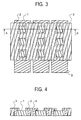
Fig. 3 is a plan view of the second embodiment of the
present invention, wherein the relations between the metal
electrode and the pixels (ITO) are illustrated.
-
Fig. 4 is a sectional view of Fig. 3 as taken along the
A-A' line.
-
Fig. 5 is a plan view of the third embodiment of the
present invention, wherein the relations between the metal
electrode and the pixels (ITO) are illustrated.
-
Fig. 6 is a sectional view of Fig. 5 as taken along the
A-A' line.
-
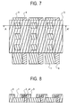
Fig. 7 is a plan view of the fourth embodiment of the
present invention, wherein the relations between the metal
electrode and the pixels (ITO) are illustrated.
-
Fig. 8 is a sectional view of Fig. 7 as taken along the
A-A' line.
DETAILED DESCRIPTION OF THE INVENTION
-
According to the present invention, there is provided
an organic EL display device comprising a pair of electrodes
and at least one organic layer interposed between the
electrodes, wherein:
- at least one of said electrodes comprises an indium
oxide-containing transparent electrode at a site
corresponding to a light emitting area, and
- a metal electrode is provided at a site other than said
site corresponding to said light emitting area, where said
metal electrode is connected to said transparent electrode,
- said metal electrode being formed of an alloy
containing Ag and/or Cu, which alloy contains at least one
metal element selected from the group consisting of at least
Rh, Pd, In, Pt and Au.
-
-
By joining such a metal electrode directly to the
transparent electrode to form a hole injecting electrode, it
is possible to keep the whole resistance value of the hole
injecting electrode low and, at the same time, dispense with
a barrier metal layer that should be located between the
transparent electrode and a conventional Al electrode, so
that the fabrication process can be simplified with a
decrease in the number of masks and fabrication cost
reductions. It is further possible to achieve a process
substantially free of hillocks that are a grave problem with
the conventional Al electrode.
-
It is also possible to dispense with any thermal
treatment process to reduce the resistance of the metal
electrode and, hence, to make use of an underlying organic
layer comprising a color filter, a color conversion film, a
flattening film and so on.
-
The transparent electrode is formed and located at
least at a site corresponding to the light emitting area
(pixel area), and connected to the metal electrode at a
junction. By the term "light emitting area" used herein is
intended an area at which a light emitting layer can give
out light, and out of which the emitted light can be taken
for use. Likewise, by the "junction with the metal
electrode" is intended an electrical junction of the
transparent electrode with the metal electrode located at
the site other than the light emitting area. The area where
the metal electrode is located is limited by the design of
an organic EL display comprising a plurality of organic EL
devices; that is, the shorter the pitch between adjacent
pixels, the narrower the area with the metal electrode
located thereon becomes. To ensure the necessary sheet
resistance, it is then required to optimize the resistivity
and film thickness of the metal electrode. The transparent
electrode area may be defined by not only the site
corresponding to the light emitting area and the junction
with the metal electrode but also the boundary between the
light emitting area and the periphery of the light emitting
area. Required for the junction with the metal electrode is
an area where sufficiently low connection resistance is
achievable.
-
For the transparent electrode, it is preferable to use
an electrode containing at least indium oxide, especially,
ITO, IZO, ZnO, SnO, In2O3 or the like, with ITO and IZO
being most preferred. For ITO, it is desired that the
mixing ratio of SnO2 with respect to In2O3 be in the range
of 1 to 20 wt%, and especially 5 to 12 wt%. For IZO, the
mixing ratio of ZnO with respect to In2O3 is preferably in
the range of 1 to 20 wt%, and especially 5 to 12 wt%.
Besides, ITO, and IZO may contain an oxide form of Sn, Ti,
Pb, etc. in an amount of up to 1% by weight as calculated on
an oxide basis.
-
Such a transparent electrode is usually used as an
anode or hole injecting electrode.
-
The transparent electrode may have at least a certain
thickness enough to inject charges such as holes, and is
usually in the range of 10 to 100 nm. However, a thickness
of 30 to 100 nm, and especially 50 to 90 nm is preferred.
At a film thickness of 100 nm or less, the transparent
electrode has so low surface roughness that its surface
properties can be improved, resulting in improvements in
light emission properties, light emission life, etc. Too
small a thickness offers problems in conjunction with film
thickness upon film formation, and the ability of the
electrode to transport holes. Too large a thickness makes
the dependence of extracted light spectra on the angle of
view likely to increase. According to the present invention,
however, it is unnecessary to increase the thickness of the
transparent electrode, thereby lowering its sheet resistance,
because the hole injecting electrode is formed of both the
transparent electrode and the metal electrode.
-
The transparent electrode should preferably have a
light transmittance of 50% or greater, especially 80% or
greater, and more especially 90% or greater with respect to
light usually in the wavelength range of 400 to 700 nm, and
especially with respect to emitted light. At too low a
transmittance, the light emitted from the light emitting
layer attenuates; it is difficult to obtain the luminance
needed for a light emitting device.
-
The metal electrode (interconnecting electrode) has a
sheet resistance of preferably 1 Ω/□ or less, and
especially 0.5 Ω/□ or less. Although there is no lower
limit to sheet resistance, a sheet resistance of about 0.1
Ω/□ is generally preferred. Preferably, the metal
electrode has a thickness of the order of preferably 10 to
2,000 nm, especially 20 to 1,000 nm, and more especially 100
to 500 nm.
-
The metal electrode is formed of an alloy containing as
the main component Ag, Cu or Ag-Cu and as the first
subordinate component one or two or more metal elements
selected from the group consisting of Pd, In, Pt and Au. It
is preferable that the alloy contains both Ag and Cu as the
main components. In this case, Cu should account for
preferably 0.1 to 5% by weight, more preferably 0.3 to 3% by
weight, and even more preferably 0.5 to 2.0% by weight of
all components. By the proper addition of Cu to Ag
improvements in corrosion resistance are achievable.
However, too little Cu makes its effect slender and too much
causes element segregation.
-
The total amount of the metal elements Rh, Pd, In, Pt
and Au added as the first subordinate component should be
preferably 0.1 to 5% by weight, more preferably 0.3 to 3.0%
by weight, and even more preferably 0.5 to 2.0% by weight
with respect to all components. Too little subordinate
components result in a corrosion resistance drop whereas too
much causes element segregation.
-
The metal electrode according to the present invention
may contain as the second subordinate component one or two
or more metal elements selected from the group consisting of
Ti, V, Cr, Mn, Fe, Co, Ni, Nb, Mo, Ta and W. In this case,
the total amount of these metal elements should be
preferably 0.1 to 5% by weight, more preferably 0.3 to 3.0%
by weight, and even more preferably 0.5 to 2.0% by weight
with respect to all components. By the addition of these
metal elements in proper amounts, improvements in corrosion
resistance are achievable. However, too little elements
make their effects slender whereas too much causes element
segregation.
-
It is acceptable to connect the metal electrode
according to the present invention to the transparent
electrode with a barrier metal layer interposed between them.
In the practice of the invention, however, it is preferable
to join the metal electrode directly to the transparent
electrode. At the junction, the transparent and metal
electrode are joined to each other usually with a metal such
as Cr or Ti or a nitride such as Ti-N, each acting as a
barrier metal, interposed between them. This is to prevent
electro-chemical corrosion from occurring between the indium
oxide-containing transparent electrode and the metal
electrode. According to the invention that can prevent any
electro-chemical corrosion between the indium oxide-containing
transparent electrode and the metal electrode,
however, it is possible to make a direct connection between
both the electrodes. By joining both the electrodes
directly to each other without recourse to any barrier metal
layer, it is possible to reduce the number of steps for film
formation and patterning and dispense with photomasking,
thereby achieving significant cost reductions.
-
Specific embodiments of the metal electrode of the
present invention and the light emitting area of the
transparent electrode that provides pixels are shown in Figs.
1 to 8.
-
Fig. 1 is illustrative of one embodiment of the present
invention. More specifically, Fig. 1 is a plan view of how
the metal electrode is actually positioned with respect to
the light emitting area of the transparent electrode that
provides pixels, and Fig. 2 is a sectional view of Fig. 1 as
taken along the A-A' line.
-
Referring to Figs. 1 and 2, a metal electrode 2 is
formed and positioned laterally of an ITO pattern 1 that is
the transparent electrode, and an insulating layer 3 is
provided in such a way as to cover these parts. The
insulating layer 3 has an opening in an ITO area defining a
pixel area. On an ITO area under the opening there is
formed an organic EL structure such as an organic layer.
-
By selective use of a metal material that can be
brought in direct contact with the ITO 1, it is thus
possible to dispose the metal electrode 2 along the ITO 1.
It is here noted that the area where the ITO 1 is in contact
with the metal electrode 2 defines a junction.
-
Fig. 3 is illustrative of another embodiment of the
present invention. More specifically, Fig. 3 is a plan view
of how the metal electrode is actually positioned with
respect to the light emitting area of the transparent
electrode that provides pixels, and Fig. 4 is a sectional
view of Fig. 3 as taken along the A-A' line.
-
Referring to Figs. 3 and 4, a metal electrode 2 is
formed and positioned in such a way as to cover an ITO
pattern 1 that is the transparent electrode, and provided
with an opening at a pixel-defining site. Then, an
insulating layer 3 is formed in such a way as to cover these
parts. In an ITO site defining the pixel area, the
insulating layer 3 has an opening slightly smaller than the
metal electrode 2. On an ITO area under the opening there
is formed an organic EL structure such as an organic layer.
-
Fig. 5 is illustrative of the third embodiment of the
present invention. More specifically, Fig. 5 is a plan view
of how the metal electrode is actually positioned with
respect to the light emitting area of the transparent
electrode that provides pixels, and Fig. 6 is a sectional
view of Fig. 5 as taken along the A-A' line. In this
embodiment, an ITO 1 is connected to a metal electrode 2
with a barrier metal layer 4 interposed between them.
-
Referring to Figs. 5 and 6, the barrier metal layer 4
is formed and positioned laterally of the ITO pattern 1 that
is the transparent electrode in such a way as to come in
contact with the ITO 1, and an insulating layer 3 is
provided in such a way as to cover the barrier layer 3. The
insulating layer 3 has an opening in an ITO area defining a
pixel area. On an ITO area under the opening there is
formed an organic EL structure such as an organic layer.
-
Fig. 7 is illustrative of the fourth embodiment of the
present invention. More specifically, Fig. 7 is a plan view
of how the metal electrode is actually positioned with
respect to the light emitting area of the transparent
electrode that provides pixels, and Fig. 8 is a sectional
view of Fig. 7 as taken along the A-A' line. In this
embodiment, an ITO 1 is connected to a metal electrode 2
with a barrier metal layer 4 interposed between them.
-
Referring to Figs. 7 and 8, the barrier metal layer 4
is formed and positioned laterally of the ITO pattern 1 that
is the transparent electrode in such a way as to come in
contact with the ITO 1, and the metal electrode 2 is formed
and positioned in such a way that it is embedded in the
barrier metal layer 4. An insulating layer 3 is then
provided in such a way as to cover these parts. The
insulating layer 3 has an opening in an ITO area defining a
pixel area. On an ITO area under the opening there is
formed an organic EL structure such as an organic layer.
-
The cathode or electron injecting electrode
corresponding to the transparent electrode of the present
invention should preferably be made up of a metal, alloy or
intermetallic compound having a work function of 4 eV or
less. A material having a work function exceeding 4 eV
results in a drop of electron injection efficiency and,
hence, a drop of light emission efficiency. For the metal
that constitutes an electron injecting electrode film having
a work function of 4 eV or less, for instance, use may be
made of alkaline metals such as Li, Na and K, alkaline earth
metals such as Li, Mg, Ca, Sr and Ba, rare earth metals such
as La and Ce, Al, In, Ag, Sn, Zn and Zr. For the alloy that
constitutes an electron injecting electrode containing a
metal having a work function of 4 eV or less, for instance,
use may be made of Ag·Mg (Ag: 1 to 20 at%), Al·Li (Li: 0.5
to 12 at%), In·Mg (Mg: 50 to 80 at%) and Al·Ca (Ca: 5 to 20
at%). These may be used alone or in combination of two or
more at any desired mixing ratio.
-
The electron injecting electrode may be formed by an
evarporation process or the like. To form the electron
injecting electrode, however, it is preferable to use
sputtering processes in general, and a DC sputtering process
in particular. Power for operating a DC sputtering system
is in the range of preferably 0.1 to 10 W/cm2, and
especially 0.5 to 7 W/cm2. The film deposition rate is
preferably in the range of 0.1 to 100 nm/min., and
especially 1 to 30 nm/min.
-
Preferably but not exclusively, inert gases such as Ar,
He, Ne, Kr and Xe or their mixtures should be used for the
sputtering gas. The sputtering pressure of such sputtering
gases should usually be in the range of about 0.1 to about
20 Pa.
-
Such an electron injecting electrode may have at least
a certain thickness enough for the injection of electrons,
e.g., of at least 1 nm, and preferably at least 3 nm. Thus,
a film thickness of the order of 3 to 500 nm is usually
preferable although there is no upper limit thereto.
-
The organic EL display device of the present invention
may have an auxiliary electrode layer on the electron
injecting electrode, i.e., on the side of the electron
injecting electrode that faces away from the organic layer.
This auxiliary electrode may be used when the film
resistance of the electron injecting electrode is high. The
auxiliary electrode may also be used, for instance, when the
electron injecting electrode is barely thick enough to
maintain its minimum electron injecting function. Further,
if the auxiliary electrode is used as an interconnecting
electrode for simple matrix, luminance variations can then
be prevented with a limited voltage drop. Furthermore, if
the auxiliary electrode is applied to an active matrix type
display using TFT, etc., it is then possible to achieve
ever-faster operation.
-
When the electron injecting electrode used has a sheet
resistance of usually 0.2 Ω/□ or greater, and especially
0.5 Ω/□ or greater, the auxiliary electrode is needed
although depending on display size and auxiliary electrode
material. Usually but not exclusively, the upper limit to
the sheet resistance is a few hundreds Ω/□. When the
electron injecting electrode used has a thickness of usually
300 nm or less, and especially 200 nm or less, too, it is
necessary to use the auxiliary electrode, although depending
on display size and auxiliary electrode material.
-
The auxiliary electrode may have at least a certain
thickness enough to make sure of electron injection
efficiency and prevent penetration of moisture, oxygen or
organic solvents, for instance, of at least 50 nm,
preferably at least 100 nm, and especially 100 to 1,000 nm.
With too thin an auxiliary electrode layer, neither are the
advantages of the invention obtainable, nor is sufficient
connection with terminal electrodes obtainable because the
ability of the auxiliary electrode layer to cover steps
becomes low. When the auxiliary electrode layer is too
thick, on the other hand, the growth rate of dark spots
becomes high because of an increase in the stress of the
auxiliary electrode layer.
-
It is also possible to use the transparent electrode as
the cathode.
-
Furthermore, the organic EL display device of the
present invention may comprise an inorganic electron
injecting layer between the cathode or electron injecting
electrode and the organic layer. By the provision of the
inorganic electron injecting electrode, it is possible to
make dramatic improvements in electron injection performance.
-
It is here noted that while the inorganic electron injecting
layer is formed of an inorganic material, yet it is usually
so thin that damage to the organic layer by a ZnO
transparent electrode can effectively prevented.
-
The inorganic electron injecting layer (inorganic
electron injecting transporting layer) comprises as a main
component one or two or more oxides selected from the group
consisting of lithium oxide (Li2O), rubidium oxide (Rb2O),
potassium oxide (K2O), sodium oxide (Na2O), cesium oxide
(Cs2O), strontium oxide (SrO), magnesium oxide (MgO) and
calcium oxide (CaO). These oxides may be used alone or in
combination of two or more at any desired mixing ratio.
Among these, strontium oxide is most preferred. Next is
magnesium oxide, calcium oxide and lithium oxide (Li2O) in
this order. Next is rubidium oxide (Rb2O), then potassium
oxide (K2O), and finally sodium oxide (Na2O). When these
oxides are mixed together for use, it is desired that 40
mol% or greater of strontium be contained in the mixture or
lithium oxide and rubidium oxide be contained in the mixture
in the total amount of 40 mol% or greater, and especially 50
mol% or greater.
-
The inorganic electron injecting layer contains as a
stabilizer silicon oxide (SiO2) and/or germanium oxide
(GeO2), which may be used alone or in a mixture form at any
desired mixing ratio.
-
Each of the aforesaid oxides is usually found in a
stoichiometric composition form. However, it is noted that
the oxide may deviate slightly from this composition; it may
have a non-stoichiometric composition.
-
The main component should account for preferably 80 to
99 mol%, and more preferably 90 to 95 mol% of all components
of the inorganic electron injecting layer, as calculated on
SrO, MgO, CaO, Li2O, Rb2O, K2O, Na2O, Cs2O, SiO2 and GeO2
bases, and the stabilizer should account for preferably 1 to
20 mol%, and more preferably 5 to 10 mol% of all the
components.
-
The inorganic electron injecting layer should have a
film thickness of preferably 0.1 to 2 nm, and more
preferably 0.3 to 0.8 nm.
-
The inorganic electron injecting layer should
preferably comprise as the first component an oxide or
oxides of
- at least one alkaline metal element having a work
function of 4 eV or less, especially 1 to 4 eV, and
preferably selected from the group consisting of Li, Na, K,
Rb, Cs and Fr, or
- at least one alkaline earth metal element having a work
function of 4 eV or less, especially 1 to 4 eV, and
preferably selected from the group consisting of Mg, Ca and
Sr, or
- at least one lanthanoid element having a work function
of 4 eV or less, especially 1 to 4 eV, and preferably
selected from the group consisting of La and Ce. Among
these oxides, lithium oxide, magnesium oxide, calcium oxide
and cerium oxide are particularly preferred. These oxides
may be used in a mixture form at any desired mixing ratio.
It is then preferable that the mixture contains lithium
oxide in an amount of 50 mol% or greater as calculated on an
Li2O basis.
-
-
Furthermore, the inorganic electron injecting layer of
high resistance comprises as the second component at least
one element selected from the group consisting of Zn, Sn, V,
Ru, Sm and In. Preferably in this case, the content of the
second component is between 0.2 mol% and 40 mol%, and
especially between 1 mol% and 20 mol%. At a smaller content
the electron injecting function becomes low wheres at a
greater content the hole blocking function becomes low.
When two or more elements are used in combination, it is
again preferable that the total content of these elements
come within the aforesaid range. The second component may
be present either in a metal element form or in an oxide
form.
-
By incorporating the second component having electrical
conductivity (low resistance) in the first component of high
resistance, the insulating substance is allowed to contain
the conductive substance in the form of islands which are
then believed to form hopping paths for electron injection.
-
While the oxide that is the first component is usually
found in a stoichiometric composition form, it is understood
that the oxide may deviate slightly from the stoichiometric
composition; it may have a non-stoichiometric composition.
The same also holds for the second component, although it is
usually present in an oxide form.
-
The inorganic electron injecting layer of high
resistance should preferably have a film thickness of the
order of 0.2 to 30 nm, and especially 0.2 to 10 nm. Any
deviation from this thickness range does not allow the
electron injecting layer to produce its own function
satisfactorily.
-
Next, the organic material layers provided in the
organic EL structure of the present invention are explained
in detail.
-
The light emitting layer comprises a multilayered film
formed of one or two or more organic compound thin films
that, at least, take part in light emitting functions.
-
The light emitting layer has functions of injecting
holes and electrons, transporting them, and recombining
holes and electrons to create excitons. For the light
emitting layer, it is preferable to use a relatively
electronically neutral compound, thereby providing easy yet
well-balanced injection and transportation of electrons and
holes.
-
In addition to the light emitting layer in a narrow
sense, the light emitting layer may comprise layers such as
a hole transporting layer of an organic material and an
electron injecting and transporting layer, if required.
-
The hole injecting and transporting layer has functions
of facilitating injection of holes from the anode or hole
injecting electrode, providing stable transportation of
holes and blocking electrons, and the electron injecting and
transporting layer has functions of facilitating injection
of electrons from the cathode or electron injecting
electrode, providing stable transportation of electrons and
blocking holes. These layers are effective for increasing
the number of holes and electrons injected into the light
emitting layer and confining holes and electrons therein for
optimizing the recombination region to improve light
emission efficiency.
-
The thickness of the light emitting layer, the hole
injecting and transporting layer, and the electron injecting
and transporting layer is not critical and varies with a
particular formation technique although it is usually of the
order of preferably 5 to 500 nm, and especially 10 to 300 nm.
-
The thickness of the hole injecting and transporting
layers, and the electron injecting and transporting layer is
equal to, or about 1/10 times to about 10 times as large as,
the thickness of the light emitting layer although it
depends on the design of the recombination/light emitting
region. When the electron injecting and transporting layer
is separated into an injecting layer and a transporting
layer, it is preferable that the injecting layer is at least
1 nm thick and the transporting layer is at least 1 nm thick.
The upper limit to thickness is usually about 500 nm for the
injecting layer and about 500 nm for the transporting layer.
The same film thickness applies when two injecting and
transporting layers are provided.
-
In the organic EL device according to the invention,
the light emitting layer contains a fluorescent material
that is a compound capable of emitting light. The
fluorescent material used herein, for instance, may be at
least one compound selected from compounds such as those
disclosed in JP-A 63-264692, e.g., quinacridone, rubrene,
and styryl dyes. Use may also be made of quinoline
derivatives such as metal complex dyes containing 8-quinolinol
or its derivative as ligands, for instance,
tris(8-quinolinolato)aluminum, tetraphenylbutadiene,
anthracene, perylene, coronene, and 12-phthaloperinone
derivatives. Use may further be made of phenylanthracene
derivatives disclosed in JP-A 8-12600, and tetraarylethene
derivatives disclosed in JP-A 8-12969.
-
Preferably, the fluorescent compound is used in
combination with a host substance capable of emitting light
by itself; that is, it is preferable that the fluorescent
compound is used as a dopant. In such a case, the content
of the fluorescent compound in the light emitting layer is
in the range of preferably 0.01 to 10% by weight, and
especially 0.1 to 5% by weight. By using the fluorescent
compound in combination with the host substance, it is
possible to vary the wavelength performance of light
emission, thereby making light emission possible on a longer
wavelength side and, hence, improving the light emission
efficiency and stability of the device.
-
Quinolinolato complexes, and aluminum complexes
containing 8-quinolinol or its derivatives as ligands are
preferred for the host substance. Such aluminum complexes
are typically disclosed in JP-A's 63-264692, 3-255190, 5-70733,
5-258859, 6-215874, etc.
-
Exemplary aluminum complexes include tris(8-quinolinolato)aluminum,
bis(8-quinolinolato)magnesium,
bis(benzo{f}-8-quinolinolato)zinc, bis(2-methyl-8-quinolinolato)aluminum
oxide, tris(8-quinolinolato)indium,
tris(5-methyl-8-quinolinolato)aluminum, 8-quinolinolato-lithium,
tris(5-chloro-8-quinolinolato)gallium, bis(5-chloro-8-quinolinolato)calcium,
5,7-dichloro-8-quinolinolato-aluminum,
tris(5,7-dibromo-8-hydroxyquinolinolato)aluminum,
and poly[zinc(II)-bis(8-hydroxy-5-quinolinyl)methane].
-
Use may also be made of aluminum complexes containing
other ligands in addition to 8-quinolinol or its derivatives,
for instance, bis(2-methyl-8-quinolinolato) (phenolato)
aluminum (III), bis(2-methyl-8-quinolinolato)(o-cresolato)
aluminum (III), bis(2-methyl-8-quinolinolato)(m-cresolato)
aluminum (III), bis(2-methyl-8-quinolinolato)(p-cresolato)
aluminum (III), bis(2-methyl-8-quinolinolato)(o-phenylphenolato)aluminum
(III), bis(2-methyl-8-quinolinolato) (m-phenylphenolato)aluminum
(III), bis(2-methyl-8-quinolinolato)
(p-phenylphenolato)aluminum (III), bis(2-methyl-8-quinolinolato)(2,3-dimethylphenolato)aluminum
(III),
bis(2-methyl-8-quinolinolato)(2,6-dimethylphenolato)aluminum
(III), bis(2-methyl-8-quinolinolato)(3,4-dimethylphenolato)aluminum
(III), bis(2-methyl-8-quinolinolato)(3,5-dimethyl-phenolato)
aluminum (III),
bis(2-methyl-8-quinolinolato)(3,5-di-tert-butylphenolato)aluminum
(III), bis(2-methyl-8-quinolinolato)(2,6-diphenylphenolato)aluminum
(III), bis(2-methyl-8-quinolinolato)(2,4,6-triphenylphenolato)aluminum
(III), bis(2-methyl-8-quinolinolato)(2,3,6-trimethyl-phenolato)aluminum
(III), bis(2-methyl-8-quinolinolato)
(2,3,5,6-tetramethylphenolato)aluminum (III), bis(2-methyl-8-quinolinolato)(1-naphtholato)aluminum
(III), bis(2-methyl-8-quinolinolato)(2-naphtholato)aluminum
(III), bis(2,4-dimethyl-8-quinolinolato)(o-phenylphenolato)aluminum
(III),
bis (2, 4-dimethyl-8-quinolinolato) (p-phenylphenolato)aluminum
(III), bis(2,4-dimethyl-8-quinolinolato)(m-phenylphenolato)
aluminum (III), bis(2,4-dimethyl-8-quinolinolato)(3,5-dimethylphenolato)aluminum
(III), bis(2,4-dimethyl-8-quinolinolato)
(3,5-di-tert-butylphenolato)aluminum (III),
bis (2-methyl-4-ethyl-8-quinolinolato) (p-cresolato)aluminum
(III), bis(2-methyl-4-methoxy-8-quinolinolato)(p-phenyl-phenolato)aluminum
(III), bis(2-methyl-5-cyano-8-quinolinolato)(o-cresolato)aluminum
(III), and bis(2-methyl-6-trifluoromethyl-8-quinolinolato)(2-naphtholato)aluminum
(III).
-
Besides, use may be made of bis(2-methyl-8-quinolinol-ato)aluminum
(III) -µ-oxo-bis(2-methyl-8-quinolinolato)
aluminum (III), bis (2,4-dimethyl-8-quinolinolato)aluminum
(III) -µ-oxo-bis(2,4-dimethyl-8-quinolinolato)aluminum (III),
bis(4-ethyl-2-methyl-8-quinolinolato)aluminum (III)-µ-oxo-bis(4-ethyl-2-methyl-8-quinolinolato)aluminum
(III), bis(2-methyl-4-methoxyquinolinolato)aluminum
(III)-µ-oxo-bis(2-methyl-4-methoxyquinolinolato)aluminum
(III), bis(5-cyano-2-methyl-8-quinolinolato)aluminum
(III)-µ-oxo-bis(5-cyano-2-methyl-8-quinolinolato)aluminum
(III), bis(2-methyl-5-trifluoromethyl-8-quinolinolato)aluminum
(III)-µ-oxo-bis(2-methyl-5-trifluoromethyl-8-quinolinolato)aluminum
(III), etc.
-
Other preferable host substances include phenyl-anthracene
derivatives disclosed in JP-A 8-12600,
tetraarylethene derivatives disclosed in JP-A 8-12969, etc.
-
In the practice of the invention, the light emitting
layer may also serve as an electron injecting and
transporting layer. In this case, it is preferable to use a
fluorescent material, e.g., tris(8-quinolinolato)aluminum or
the like, which may be provided by evaporation.
-
If necessary or preferably, the light emitting layer is
formed of a mixed layer of at least one compound capable of
injecting and transporting holes with at least one compound
capable of injecting and transporting electrons. Preferably
in this case, a dopant is incorporated in the mixed layer.
The content of the dopant compound in the mixed layer is in
the range of preferably 0.01 to 20% by weight, and
especially 0.1 to 15% by weight.
-
In the mixed layer with a hopping conduction path
available for carriers, each carrier migrates in the polarly
prevailing substance, so making the injection of carriers
having an opposite polarity unlikely to occur. This leads
to an increase in the service life of the device due to less
damage to the organic compound. By incorporating the
aforesaid dopant in such a mixed layer, it is possible to
vary the wavelength performance of light emission that the
mixed layer itself possesses, thereby shifting the
wavelength of light emission to a longer wavelength side and
improving the intensity of light emission, and the stability
of the device as well.
-
The compound capable of injecting and transporting
holes and the compound capable of injecting and transporting
electrons, both used to form the mixed layer, may be
selected from compounds for the injection and transportation
of holes and compounds for the injection and transportation
of electrons, as will be described later. Especially for
the compounds for the injection and transportation of holes,
it is preferable to use amine derivatives having strong
fluorescence, for instance, hole transporting materials such
as triphenyldiamine derivatives, styrylamine derivatives,
and amine derivatives having an aromatic fused ring.
-
For the compounds capable of injecting and transporting
electrons, it is preferable to use metal complexes
containing quinoline derivatives, especially 8-quinolinol or
its derivatives as ligands, in particular, tris(8-quinolinolato)
aluminum (Alq3). It is also preferable to
use the aforesaid phenylanthracene derivatives, and
tetraarylethene derivatives.
-
For the compounds for the injection and transportation
of holes, it is preferable to use amine derivatives having
strong fluorescence, for instance, hole transporting
materials such as triphenyldiamine derivatives, styrylamine
derivatives, and amine derivatives having an aromatic fused
ring.
-
In this case, the ratio of mixing the compound capable
of injecting and transporting holes with the compound
capable of injecting and transporting electrons is
determined while the carrier mobility and carrier density
are taken into consideration. In general, however, it is
preferred that the weight ratio between the compound capable
of injecting and transporting holes and the compound capable
of injecting and transporting electrons is of the order of
1/99 to 99/1, particularly 10/90 to 90/10, and more
particularly 20/80 to 80/20.
-
Preferably, the thickness of the mixed layer should be
equal to or greater than the thickness of a single molecular
layer, and less than the thickness of the organic compound
layer. More specifically, the mixed layer has a thickness
of preferably 1 to 85 nm, especially 5 to 60 nm, and more
especially 5 to 50 nm.
-
Preferably, the mixed layer is formed by co-evaporation
where the selected compounds are evaporated from different
evaporation sources. When the compounds to be mixed have
identical or slightly different vapor pressures (evaporation
temperatures), however, they may have previously been mixed
together in the same evaporation boat for the subsequent
evaporation. Preferably, the compounds are uniformly mixed
together in the mixed layer. However, the compounds in an
island archipelagic form may be present in the mixed layer.
The light emitting layer may generally be formed at a given
thickness by the evaporation of the organic fluorescent
substance or coating a dispersion of the organic fluorescent
substance in a resin binder.
-
For the hole injecting and transporting layer, use may
be made of various organic compounds as disclosed in JP-A's
63-295695, 2-191694, 3-792, 5-234681, 5-239455, 5-299174, 7-126225,
7-126226 and 8-100172 as well as EP 0650955A1.
Examples are tetraarylbenzidine compounds (triaryldiamine or
triphenyldiamine (TPD)), aromatic tertiary amines, hydrazone
derivatives, carbazole derivatives, triazole derivatives,
imidazole derivatives, oxadiazole derivatives having an
amino group, and polythiophenes. These compounds may be
used alone or in combination of two or more. Where these
compounds are used in combination of two or more, they may
be stacked as separate layers, or otherwise mixed.
-
When the hole injecting and transporting layer is
provided as a separate hole injecting layer and a separate
hole transporting layer, two or more compounds are selected
in a preferable combination from the compounds already
mentioned for the hole injecting and transporting layer. In
this regard, it is preferred to laminate layers in such an
order that a compound layer having a lower ionization
potential is disposed nearest to the hole injecting
electrode (ITO, etc.). It is also preferred to use a
compound having good thin film forming ability at the hole
injecting electrode surface. This order of lamination holds
for the provision of two or more hole injecting and
transporting layers, and is effective as well for lowering
driving voltage and preventing the occurrence of current
leakage and the appearance and growth of dark spots. Since
evaporation is utilized in the manufacture of devices, films
as thin as about 1 to 10 nm can be formed in a uniform and
pinhole-free state, which restrains any change in color tone
of light emission and a drop of efficiency by re-absorption
even if a compound having a low ionization potential and
absorption in the visible range is used in the hole
injecting layer. Like the light emitting layer and so on,
the hole injecting and transporting layer or layers may be
formed by evaporating the aforesaid compounds.
-
For the electron injecting and transporting layer that
is preferably provided, there may be used quinoline
derivatives such as organic metal complexes containing 8-quinolinol
or its derivatives as ligands, for instance,
tris(8-quinolinolato)aluminum (Alq3), oxadiazole derivatives,
perylene derivatives, pyridine derivatives, pyrimidine
derivatives, quinoxaline derivative, diphenylquinone
derivatives, and nitro-substituted fluorene derivatives.
The electron injecting and transporting layer may also serve
as a light emitting layer. In this case, it is preferable
to use tris(8-quinolilato)aluminum, etc. As is the case
with the light emitting layer, the electron injecting and
transporting layer may then be formed by evaporation or the
like.
-
Where the electron injecting and transporting layer is
a double-layered structure comprising an electron injecting
layer and an electron transporting layer, two or more
compounds are selected in a preferably combination from the
compounds commonly used for electron injecting and
transporting layers. In this regard, it is preferred to
laminate layers in such an order that a compound layer
having a greater electron affinity is disposed nearest to
the electron injecting electrode. This order of lamination
also applies where a plurality of electron injecting and
transporting layers are provided.
-
To form the hole injecting and transporting layer, the
light emitting layer and the electron injecting and
transporting layer, it is preferable to use a vacuum
evaporation technique which enables a homogeneous thin film
to be obtained. According to the vacuum evaporation process,
it is possible to obtain homogeneous thin films in an
amorphous state or with a crystal grain diameter of at most
0.2 µm. The use of a thin film having a crystal grain
diameter exceeding 0.2 µm results in non-uniform light
emission. To avoid this, it is required to increase the
driving voltage of the device; however, there is a striking
drop of hole injection efficiency.
-
No particular limitation is imposed on vacuum
evaporation conditions. However, an evaporation rate of the
order of 0.01 to 1 nm/sec. is preferably applied at a degree
of vacuum of 10-4 Pa or lower. It is also preferable to
form the layers continuously in vacuum. If the layers are
continuously formed in vacuum, high properties are then
obtained because the adsorption of impurities on the
interface between the adjacent layers can be avoided.
Furthermore, the driving voltage of the device can be
lowered while the occurrence and growth of dark spots are
inhibited.
-
When the vacuum evaporation process is used to form the
layers, each containing a plurality of compounds, it is
preferable to carry out co-evaporation while boats charged
with the compounds are individually placed under temperature
control.
-
For the substrate on which an organic EL structure is
formed according to the present invention, amorphous
substrates such as glass and quartz substrates, and crystal
substrates made up of Si, GaAs, ZnSe, ZnS, GaP or InP may be
used. These crystal substrates may be provided thereon with
a crystalline or non-crystalline metal buffer layer. For
the metal substrate, Mo, Al, Pt, Ir, Au, Pd, etc. may be
used. However, preference is given to a glass substrate.
The substrate, when it is located on the side out of which
light is taken out, should preferably be transparent to
ligth as is the case with the aforesaid electrode.
-
Preferably, the device is sealed up by means of a
sealing sheet, etc. for the purpose of preventing oxidation
of the organic layers and electrodes in the device. To
prevent penetration of moisture, the sealing sheet is bonded
to the device using an adhesive resin layer to seal up the
device. An inert gas such as Ar, He, and N2 is preferably
used as a sealing gas. Then, the sealing gas should
preferably have a moisture content of up to 100 ppm,
especially up to 10 ppm, and more especially up to 1 ppm.
Although there is no particular lower limit to the moisture
content, the sealing gas should usually have a moisture
content of about 0.1 ppm.
-
The sealing sheet, preferably in a flat sheet form, may
be made of transparent or translucent materials such as
glasses, quartz, and resins, among which the glasses are
preferred. For such glass materials, alkali glass is
preferable from a cost standpoint. Other preferable glass
materials, for instance, include soda lime glass, lead
alkali glass, borosilicate glass, aluminosilicate glass, and
silica glass. In particular, a soda glass material
subjected to no surface treatment is inexpensive and so is
preferable. A metal sheet, a plastic sheet, etc., too, may
be used in place of the sealing glass sheet.
-
For height control, a spacer is used to keep the
sealing sheet at a height as desired. The spacer material
may be resin beads, silica beads, glass beads, glass fibers,
etc., with the glass beads being most preferred. The spacer
may or may not be used when a recess is provided in the
sealing sheet.
-
The spacer may have been incorporated in the sealing
adhesive agent or may be incorporated in the sealing
adhesive agent at the time of bonding. The content of the
spacer in the sealing adhesive agent should be preferably
0.01 to 30 wt%, and more preferably 0.1 to 5 wt%.
-
For the adhesive agent, it is preferable to use a
cation curing epoxy resin of the ultraviolet curing type,
although an adhesive agent of the type that ensures stable
adhesion strength and good airtightness may be used.
-
A color filter film or a fluorescent materialcontaining
color conversion film or a dielectric reflecting
film may be used together with the substrate for control of
emitted colors.
-
For the color filter film, a color filter employed with
liquid crystal display devices may be used. However, it is
preferable to control the properties of the color filter in
conformity to the light emitted from the organic EL device,
thereby optimizing the efficiency of taking out light
emission and color purity.
-
By using a color filter capable of cutting off
extraneous light of such short wavelength as absorbed by the
EL device material or the fluorescent conversion layer, it
is possible to improve the light resistance of the device
and the contrast of what is displayed on the device.
-
Instead of the color filter, an optical thin film such
as a dielectric multilayer film may be used.
-
The fluorescent color conversion film absorbs light
emitted from an EL device and gives out light from the
phosphors contained therein for the color conversion of
light emission, and is composed of three components, a
binder, a fluorescent material and a light absorbing
material.
-
In the practice of the invention, it is basically
preferable to use a fluorescent material having high
fluorescent quantum efficiency, and especially a fluorescent
material having strong absorption in an EL light emission
wavelength region. Laser dyes are suitable for the practice
of the invention. To this end, for instance, it is
preferable to use rohodamine compounds, perylene compounds,
cyanine compounds, phthalocyanine compounds (including
subphthalocyanine compounds, etc.), naphthaloimide compounds,
fused cyclic hydrocarbon compounds, fused heterocyclic
compounds, styryl compounds, and coumarin compounds.
-
For the binder, it is basically preferable to make an
appropriate selection from materials that do not extinguish
fluorescence. It is particularly preferable to use a
material that can be finely patterned by photolithography,
printing or the like. It is also preferable to use a
material that is not damaged during hole injecting electrode
(e.g., ITO or IZO) film formation.
-
The light absorbing material is used when light is not
fully absorbed by the fluorescent material, and so may be
dispensed with, if not required. For the light absorbing
material, it is preferable to make a selection from
materials that do not extinguish the fluorescence of the
fluorescent material.
-
The organic EL display device of the present invention
is generally of the DC or pulse drive type while it may be
of the AC drive type. The applied voltage is generally of
the order of 2 to 30 volts.
EXAMPLE
-
The present invention is explained more specifically
with reference to some illustrative examples.
Example 1
-
A glass substrate was provided thereon with a 100-nm
thick ITO transparent electrode, and stripes of 280 µm in
width and 24 mm in length were patterned on the ITO
transparent electrode at an interval of 20 µm and according
to an array of 256 lines. Then, a barrier metal layer or
Ti-N layer and a metal electrode layer or Ag-Pd (Pd: 2.5% by
weight) alloy layer were continuously formed to a thickness
of 50 nm and a thickness of 300 nm, respectively. Then, Ti-N
layers of 20 µm in width were formed on one side of the
ITO transparent electrode stripes in such a way that they
overlapped each other at a width of 5 µm. Then, an Ag-Pd
layer of 10 µm in width was formed by patterning on the Ti-N
layer, thereby forming a hole injecting electrode stripe
pattern comprising an ITO transparent electrode, an Ag-Pd
metal electrode formed on its one side and a Ti-N barrier
metal layer interposed between them. At this time, the ITO
transparent electrode, Ti-N barrier metal layer and Ag-Pd
metal electrode were found to have a sheet resistance of 50
Ω/□, 40 Ω/□ and 0.13 Ω/□, respectively. The hole
injecting electrode was found to have an interconnecting
resistance of 300 Q per line.
-
Thereafter, an insulating layer was formed and
patterned so as to provide insulation of an area other than
light emitting areas, and openings of 260 x 260 µm2 in size
were formed on the insulating layer at an interval of 40 µm
and according to an array of 64 dots x 256 lines, thereby
forming the light emitting areas. Furthermore, a device
separating structure was formed according to a given pattern
at right angles with the hole injecting electrode stripes.
The thus obtained substrate was ultrasonically washed with
neutral detergent, warm pure water and super-pure water, and
then dried by an air knife using destaticized and heated
nitrogen. During the process mentioned above, no hillocks
were found in the metal electrode.
-
Then, the substrate was cleaned on its surface with
UV/O3, and fixed to a substrate holder in a vacuum
evaporation system, which was evacuated to a vacuum of 1 x
10-4 Pa or lower. M-MTDATA or N,N-diphenyl-N,N'-m-tolyl-4,4',4''-tris-(N-(3-methylphenyl)-N-phenylamino)triphenylamine
was deposited by evaporation at a
deposition rate of 0.2 nm/sec. to a thickness of 40 nm,
thereby forming a hole injecting layer. With the vacuum
still maintained, TPD or N,N'-diphenyl-N,N'-m-tolyl-4,4'-diamino-1,1'-biphenyl
was then deposited by evaporation at a
deposition rate of 0.2 nm/sec. to a thickness of 35 nm,
thereby forming a hole transporting layer. With the vacuum
still kept, Alq3 was deposited by evaporation at a
deposition rate of 0.2 nm/sec. to a thickness of 50 nm,
thereby forming a combined electron injecting/transporting
and light emitting layer. With the vacuum still kept, MgAg
was deposited by co-evaporation (binary evaporation) at an
evaporation rate ratio of Mg:Ag = 10:1 to a thickness of 200
nm, thereby forming an electron injecting layer. This
electron injecting electrode was isolated and insulated by
the given pattern of device separating structure, so that it
could be positioned at right angles with the hole injecting
electrode. At sites other than the light emitting areas,
the electron injecting electrode was completely insulated
from the hole injecting electrode by the insulating layer
formed on the hole injecting electrode.
-
The thus assembled organic EL device was driven in a
dry air atmosphere in such a way that a luminance of 100
cd/m2 was obtained. Luminance of the device from the
current feed side to the opposite side was measured using
the range of 7 dots x 7 lines as one measure unit. As a
result, it was found that throughout the areas measured,
light emission luminance variations with respect to the
time-average light emission luminance of 100 cd/m2 on the
current feed side were within -5%. From this, it was
understood that there is no considerable influence of
voltage drops even on a large-area screen display.
Comparative Example 1
-
An organic EL device was obtained as in Example 1 with
the exception that instead of Ag-Pd, Al was used as the
metal electrode. During the substrate fabrication process,
hillocks were found in the Al metal electrode. From the
fact that the reverse bias withstand voltage of the organic
EL device was low, it was found that this comparative
example was inferior in durability than Example 1.
Comparative Example 2
-
An organic EL device was obtained as in Example 1 with
the exception that instead of Ag-Pd, an Al-Ti (Ti: 2.5% by
weight) alloy was used as the metal electrode. During the
substrate fabrication process, no hillocks were found in the
Al-Ti metal electrode. The Al-Ti metal electrode had a
sheet resistance of 0.3 Ω/□, and the hole injecting
electrode had an interconnecting resistance of 600 Ω per
line. The obtained organic EL device was driven and
estimated as in Example 1. As a consequence, it was found
that some areas of the device showed light emission
luminance variations of greater than -5% with respect to the
time-average light emission luminance of 100 cd/m2 on the
current feed side.
Example 2
-
An organic EL device was obtained as in Example 1 with
the exception that any barrier metal layer was not formed at
all. During the substrate fabrication process, no
particular problem was found. The hole injecting electrode
had an interconnecting resistance of 300 Ω per line as was
the case with Example 1. The obtained organic EL device was
driven and estimated as in Example 1. The results were
substantially the same as in Example 1. In this example,
any photomask for the barrier metal layer was not used and
the step of forming the barrier metal layer was omitted. As
a result, about 3% cost reductions was achieved as compared
with Example 1.
Example 3
-
An organic EL device was obtained as in Example 2 with
the exception that instead of Ag-Pd, an Ag-In (In: 2.5% by
weight) alloy was used as the metal electrode. At this time,
the hole injecting electrode had an interconnecting
resistance of 300 Ω per line. The obtained organic EL
device was driven and estimated as in Example 2. The
results were substantially the same as in Example 2.
Example 4
-
An organic EL device was obtained as in Example 2 with
the exception that instead of Ag-Pd, a Cu-Pd (Pd: 2.5% by
weight) alloy was used as the metal electrode. At this time,
the hole injecting electrode had an interconnecting
resistance of 300 Ω per line. The obtained organic EL
device was driven and estimated as in Example 2. The
results were substantially the same as in Example 2.
Comparative Example 3
-
A hole injecting electrode was prepared as in Example 1
with the exception that instead of Ag-Pd, Al was used as the
metal electrode. The ITO transparent electrode could not
well be joined to the Al metal electrode, and the ITO
transparent electrode underwent electro-chemical corrosion
due to battery reactions occurred between ITO and Al during
the process. It was thus impossible to obtain a substrate
for an organic EL device.
Comparative Example 4
-
An organic El device was obtained as in Example 2 with
the exception that no metal electrode layer was formed. At
this time, the hole injecting electrode had an
interconnecting resistance of 4 kΩ per line. The obtained
organic EL device was driven and estimated as in Example 2.
As a result, it was found that the device showed a luminance
variation of a high -20% with respect to the time-average
light emission luminance of 100 cd/m2 on the current feed
side.
Comparative Example 5
-
An organic EL device was obtained as in Comparative
Example 4 with the exception that the thickness of the ITO
transparent electrode was changed to 1,500 nm. At this time,
the ITO transparent electrode had a sheet resistance 3.3 Ω/
□, and the hole injecting electrode had an interconnecting
resistance of 300 Ω per line as was the case with Example 2.
The obtained organic EL device was driven and estimated as
in Example 2. As a result, it was found that the spectra of
the extracted light varied, and the luminance was lower than
that of Example 2 when compared on the same driving current
level. From the fact that the reverse bias withstand
voltage of the device was low, it was also found that this
comparative example was inferior in durability than Example
2. On the other hand, this device was driven for 5,000
hours. As a result, it was found that the density of dark
spots observed was about 5 times as high as that in Example
2, showing reliability drops.
Comparative Example 6
-
An organic EL device was obtained as in Example 2 with
the exception that instead of Ag-Pd, Ag was used as the
metal electrode. At this time, the ITO transparent
electrode had a sheet resistance of 0.08 Ω/□, and the hole
injecting electrode had an interconnecting resistance of 200
Ω per line, which figure was lower than that in Example 2.
The obtained organic EL device was driven and estimated as
in Example 2. As a result, it was found that throughout the
areas measured in the initial stage, light emission
luminance variations with respect to the time-average light
emission luminance of 100 cd/m2 on the current feed side
were all within -4%. After the lapse of 5,000 hours,
however, a luminance change of -10% at most was observed.
Example 5
-
An organic EL device was obtained as in Example 2 with
the exception that instead of Ag-Pd, an Ag-Pd-Cu (Pd: 2.5%
by weight - Cu: 2.5% by weight) alloy was used as the metal
electrode. At this time, the hole injecting electrode had
an interconnecting resistance of 300 Ω per line. The
obtained organic EL device was driven and estimated as in
Example 2. The results were much the same as in Example 2.
It was also found that a margin wider than in Example 2
could be obtained to set up process conditions concerning
the baking temperature, developer concentration, etching
solution concentration, etc. for the fabrication of the
substrate for this device.
Example 6
-
An organic EL device was obtained as in Example 2 with
the exception that instead of Ag-Pd, an Ag-Pd-Ti (Pd: 2.5%
by weight - Ti: 2.5% by weight) alloy was used as the metal
electrode. At this time, the hole injecting electrode had
an interconnecting resistance of 300 Ω per line. The
obtained organic EL device was driven and estimated as in
Example 2. The results were much the same as in Example 2.
It was also found that a margin wider than in Example 2
could be obtained to set up process conditions concerning
the baking temperature, developer concentration, etching
solution concentration, etc. for the fabrication of the
substrate for this device.
Example 7
-
An organic EL device was obtained as in Example 2 with
the exception that instead of Ag-Pd, an Ag-Pd-Cr (Pd: 2.5%
by weight - Cr: 2.5% by weight) alloy was used as the metal
electrode. At this time, the hole injecting electrode had
an interconnecting resistance of 300 Ω per line. The
obtained organic EL device was driven and estimated as in
Example 2. The results were much the same as in Example 2.
It was also found that a margin wider than in Example 2
could be obtained to set up process conditions concerning
the baking temperature, developer concentration, etching
solution concentration, etc. for the fabrication of the
substrate for this device.
Example 8
-
An organic EL device was obtained as in Example 5 with
the exception that the composition ratio of the metal
electrode Ag-Pd-Cu was changed to Pd = 1.25% by weight - Cu
= 1.25% by weight. At this time, the hole injecting
electrode had an interconnecting resistance of 300 Ω per
line. The obtained organic EL device was driven and
estimated as in Example 5. The results were much the same
as in Example 5. It was also found that in Example 5, too,
a wider margin could be obtained to set up process
conditions concerning the baking temperature, developer
concentration, etching solution concentration, etc. for the
fabrication of the substrate for this device.
Example 9
-
An organic EL device was obtained as in Example 8 with
the exception that the thickness of the ITO transparent
electrode was changed to 150 nm. The obtained organic EL
device was driven and estimated as in Example 8. The
results were much the same as in Example 8.
Example 10
-
An organic EL device was obtained as in Example 8 with
the exception that the thickness of the ITO transparent
electrode was changed to 50 nm. The obtained organic EL
device was driven and estimated as in Example 8. The
results were much the same as in Example 8. At this time,
the hole injecting electrode had an interconnecting
resistance of 300 Ω per line as was the case with Example 8.
After the device had been driven for 5,000 hours, it was
found that the density of dark spots measured was 1/2 or
less of that in Example 8; some considerable improvements
were obtained in reliability.
Example 11
-
An organic EL device was obtained as in Example 8 with
the exception that an IZO transparent electrode was used as
the transparent electrode. The obtained organic EL device
was driven and estimated as in Example 8. The results were
much the same as in Example 8.
Example 12
-
Example 3 was repeated with proviso that Rh, Pt, and Au
was used in place of In. In any case, the results were much
the same as in Example 3.
Example 13
-
Example 6 was repeated with proviso that V, Mn, Fe, Co,
Ni, Nb, Mo, Ta, and W was used in place of Ti. In any case,
the results were much the same as in Example 6.
ADVANTAGES OF THE INVENTION
-
According to the present invention, it is possible to
achieve a high-quality yet low-cost organic EL display
device by lowering the wiring resistance of a transparent
electrode, improving the dependence of extracted spectra on
the angle of field, stabilizing a fabrication process due to
prevention of hillocks, and dispensing with any barrier
metal layer, thereby achieving considerable cost reductions.
-
While the invention has been described with reference
to preferred embodiments, it will be obvious to those
skilled in the art that various changes may be made and
equivalents may be substituted for elements thereof without
departing from the scope of the invention. In addition,
many modifications may be made to adapt a particular
situation or material to the teachings of the invention
without departing from the essential scope thereof.
Therefore, it is intended that the invention not be limited
to the particular embodiments disclosed as the best mode
contemplated for carrying out the invention, but that the
invention will include all embodiments falling within the
scope of the appended claims.