EP1107068A2 - Lithographic projection apparatus with system for positioning a reflector - Google Patents
Lithographic projection apparatus with system for positioning a reflector Download PDFInfo
- Publication number
- EP1107068A2 EP1107068A2 EP00310370A EP00310370A EP1107068A2 EP 1107068 A2 EP1107068 A2 EP 1107068A2 EP 00310370 A EP00310370 A EP 00310370A EP 00310370 A EP00310370 A EP 00310370A EP 1107068 A2 EP1107068 A2 EP 1107068A2
- Authority
- EP
- European Patent Office
- Prior art keywords
- orientation
- reflective optical
- sensing means
- constructed
- optical elements
- Prior art date
- Legal status (The legal status is an assumption and is not a legal conclusion. Google has not performed a legal analysis and makes no representation as to the accuracy of the status listed.)
- Granted
Links
Images

Classifications
-
- G—PHYSICS
- G03—PHOTOGRAPHY; CINEMATOGRAPHY; ANALOGOUS TECHNIQUES USING WAVES OTHER THAN OPTICAL WAVES; ELECTROGRAPHY; HOLOGRAPHY
- G03F—PHOTOMECHANICAL PRODUCTION OF TEXTURED OR PATTERNED SURFACES, e.g. FOR PRINTING, FOR PROCESSING OF SEMICONDUCTOR DEVICES; MATERIALS THEREFOR; ORIGINALS THEREFOR; APPARATUS SPECIALLY ADAPTED THEREFOR
- G03F7/00—Photomechanical, e.g. photolithographic, production of textured or patterned surfaces, e.g. printing surfaces; Materials therefor, e.g. comprising photoresists; Apparatus specially adapted therefor
- G03F7/70—Microphotolithographic exposure; Apparatus therefor
- G03F7/70216—Mask projection systems
- G03F7/70258—Projection system adjustments, e.g. adjustments during exposure or alignment during assembly of projection system
-
- G—PHYSICS
- G03—PHOTOGRAPHY; CINEMATOGRAPHY; ANALOGOUS TECHNIQUES USING WAVES OTHER THAN OPTICAL WAVES; ELECTROGRAPHY; HOLOGRAPHY
- G03F—PHOTOMECHANICAL PRODUCTION OF TEXTURED OR PATTERNED SURFACES, e.g. FOR PRINTING, FOR PROCESSING OF SEMICONDUCTOR DEVICES; MATERIALS THEREFOR; ORIGINALS THEREFOR; APPARATUS SPECIALLY ADAPTED THEREFOR
- G03F7/00—Photomechanical, e.g. photolithographic, production of textured or patterned surfaces, e.g. printing surfaces; Materials therefor, e.g. comprising photoresists; Apparatus specially adapted therefor
- G03F7/70—Microphotolithographic exposure; Apparatus therefor
- G03F7/70058—Mask illumination systems
- G03F7/702—Reflective illumination, i.e. reflective optical elements other than folding mirrors, e.g. extreme ultraviolet [EUV] illumination systems
Definitions
- the present invention relates to lithographic projection apparatus comprising:
- the projection system may hereinafter be referred to as the "lens"; however, this term should be broadly interpreted as encompassing various types of projection system, including refractive optics, reflective optics, and catadioptric systems, for example.
- the illumination system may also include elements operating according to any of these principles for directing, shaping or controlling the projection beam of radiation, and such elements may also be referred to below, collectively or singularly, as a “lens”.
- the first and second object tables may be referred to as the "mask table” and the "substrate table", respectively.
- the mask table should be taken as any structure or device that may or does hold another structure or device, generally referred to as a mask, in which a pattern to be imaged is or can be formed.
- the lithographic apparatus may be of a type having two or more mask tables and/or two or more substrate tables. In such "multiple stage" devices the additional tables may be used in parallel, or preparatory steps may be carried out on one or more stages while one or more other stages are being used for exposures.
- Lithographic projection apparatus can be used, for example, in the manufacture of integrated circuits (ICs).
- the mask reticle
- the mask may contain a circuit pattern corresponding to an individual layer of the IC, and this pattern can be imaged onto a target area (comprising one or more dies) on a substrate (silicon wafer) which has been coated with a layer of radiation-sensitive material (resist).
- a target area comprising one or more dies
- a substrate silicon wafer
- a layer of radiation-sensitive material resist
- a single wafer will contain a whole network of adjacent target areas which are successively irradiated via the mask, one at a time.
- each target area is irradiated by exposing the entire mask pattern onto the target area in one go; such an apparatus is commonly referred to as a wafer stepper.
- each target area is irradiated by progressively scanning the mask pattern under the projection beam in a given reference direction (the "scanning" direction) while synchronously scanning the substrate table parallel or anti-parallel to this direction; since, in general, the projection system will have a magnification factor M (generally ⁇ 1), the speed V at which the substrate table is scanned will be a factor M times that at which the mask table is scanned. More information with regard to lithographic devices as here described can be gleaned from International Patent Application WO 97/33205.
- apparatus of this type contained a single first object (mask) table and a single second object (substrate) table.
- first object mask
- second object substrate
- machines are becoming available in which there are at least two independently movable substrate tables; see, for example, the multi-stage apparatus described in International Patent Applications WO 98/28665 and WO 98/40791.
- the basic operating principle behind such multi-stage apparatus is that, while a first substrate table is underneath the projection system so as to allow exposure of a first substrate located on that table, a second substrate table can run to a loading position, discharge an exposed substrate, pick up a new substrate, perform some initial metrology steps on the new substrate, and then stand by to transfer this new substrate to the exposure position underneath the projection system as soon as exposure of the first substrate is completed, whence the cycle repeats itself; in this manner, it is possible to achieve a substantially increased machine throughout, which in turn improves the cost of ownership of the machine.
- wavelengths of less than about 200 nm for example 193 nm, 157 nm or 126 nm.
- Further reductions in the wavelength of the illumination radiation e.g to about 10 to 20 nm, are also envisaged.
- Such wavelengths in particular are more conveniently focused and controlled by reflective optics, such as mirrors.
- mirrors in lithography apparatus must be positioned to especially high accuracy, as compared to refractive elements, because any rotational orientation errors are magnified by the total downstream optical path length.
- the optical path length may be of the order of 2 m or more.
- a lithographic projection apparatus comprising:
- the one or more reflective optical elements may comprise a single element such as a mirror, a reflective grating, a reflective filter, etc. or a combination of such elements with or without other types of element.
- the position of the reflective optics is controlled continuously or repeatedly during operation of the apparatus and the effects of vibrations and mechanical shocks, and thermal and mechanical drift thereby can be mitigated.
- the projection apparatus further comprises sensing means constructed and arranged to determine a change in position and/or orientation of one or more of said reflective optical elements, and to output one or more position signals indicative thereof; and said positioning means comprises:
- the lithographic apparatus includes a reference frame and sensing means for determining the position of said reflective optics relative to said reference frame.
- the sensing means comprises:
- the positioning system can accurately position, or stabilize, the reflective optics without a lengthy calibration or initialization procedure, and counteract any vibrations in the reflective optics.
- the drive means are controlled primarily on the basis of the high frequency output from the relative sensing means or interferential encoders.
- the absolute sensing means preferably include one or more capacitive or inductive sensors and the relative position sensing means preferably include one or more interferometers.
- said sensing means is constructed and arranged to direct a sensing beam of radiation separate from said projection beam along said one or more reflective optical elements; and to determine a position of said sensing beam when having been reflected by said one or more reflective optical elements.
- a method of manufacturing a device using a lithographic projection apparatus comprising:
- a pattern in a mask is imaged onto a substrate which is at least partially covered by a layer of radiation-sensitive material (resist).
- the substrate Prior to this imaging step, the substrate may undergo various procedures, such as priming, resist coating and a soft bake. After exposure, the substrate may be subjected to other procedures, such as a post-exposure bake (PEB), development, a hard bake and measurement/inspection of the imaged features.
- PEB post-exposure bake
- This array of procedures is used as a basis to pattern an individual layer of a device, e.g. an IC.
- Such a patterned layer may then undergo various processes such as etching, ion-implantation (doping), metallisation, oxidation, chemo-mechanical polishing, etc., all intended to finish off an individual layer. If several layers are required, then the whole procedure, or a variant thereof, will have to be repeated for each new layer. Eventually, an array of devices will be present on the substrate (wafer). These devices are then separated from one another by a technique such as dicing or sawing, whence the individual devices can be mounted on a carrier, connected to pins, etc. Further information regarding such processes can be obtained, for example, from the book “Microchip Fabrication: A Practical Guide to Semiconductor Processing", Third Edition, by Peter van Zant, McGraw Hill Publishing Co., 1997, ISBN 0-07-067250-4.
- the terms “radiation” and “beam” are used to encompass all types of electromagnetic radiation, including, for example, ultraviolet radiation, EUV and X-rays.
- the terms “mirror” and “reflector” are used synonymously and, unless the context otherwise determines, are intended to encompass any reflective element, whether wholly, partially or selectively reflective and whether or not it has any other optical, e.g. refractive or diffractive, properties. Where the context allows, the term may also apply to non-specular reflectors such as scatter plates.
- position should be interpreted broadly as referring to any or all of the X, Y, and Z positions and rotational positions Rx, Ry and Rz.
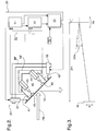
- Figure 1 schematically depicts a lithographic projection apparatus according to the invention.
- the apparatus comprises:
- the radiation system comprises a source LA (e.g. a Hg lamp, an excimer laser, a laser or discharge plasma source, or an undulator provided around the path of an electron beam in a storage ring or synchrotron) which produces a beam of radiation.
- a source LA e.g. a Hg lamp, an excimer laser, a laser or discharge plasma source, or an undulator provided around the path of an electron beam in a storage ring or synchrotron
- This beam is passed along various optical components included in illumination system IL so that the resultant beam PB is collected in such a way as to give a desired illumination profile at the entrance pupil and the mask.
- the beam PB subsequently impinges upon the mask MA which is held in a mask holder on a mask table MT. Having been selectively reflected by the mask MA, the beam PB passes through the lens PL, which focuses the beam PB onto a target area C of the substrate W.
- the substrate table WT can be moved accurately, e.g. so as to position different target areas C in the path of the beam PB.
- the interferometric displacement measuring means IF and the first positioning means PM can be used to accurately position the mask MA with respect to the path of the beam PB.
- movement of the object tables MT, WT can be realized with the aid of a long-stroke module (course positioning) and a short stroke module (fine positioning), which are not explicitly depicted in Figure 1.
- the depicted apparatus can be used in two different modes:
- the present embodiment employs a reflective mask
- the present invention may also be used in lithographic apparatus having transmissive masks.
- the depicted embodiment also employs reflective elements in the radiation and projections systems, however some refractive elements may also be used.
- FIG. 2 illustrates one of the mirrors 10 included in the illumination optics IL or projection optics PL and its associated positioning system 20, which comprises drive system 30, position sensing system 40 and control system 50.
- Mirror 10 is depicted for clarity as a flat mirror set at an acute angle to the incident radiation PB.
- mirror 10 may be a glancing incidence mirror and may be macro- or microscopically shaped to effect any desired shaping or focusing of the radiation beam PB.
- mirror 10 is mounted on drives 31, 32 which form part of the positioning system 30 and which in turn are mounted on base frame BF.
- Base frame BF is desirably very solid and may be attached to, or part of, the base plate BP of the lithographic apparatus 1, for example.
- Drives 31, 32 are used to accurately control the position, and particularly the orientation, of the mirror. For clarity, only two drives are illustrated in Figure 2 but it will be appreciated that more or fewer drives may be provided to control the position of the mirror in any or all of the six degrees of freedom.
- the drives 31, 32 comprise Lorentz-force motors, of which the general working principle, for instance, is disclosed in European patent application EP 1 001 512 and equivalent US patent application US 09/435,638, which are incorporated herein by reference.
- Other suitable actuators or motors having a low stiffness and the necessary responsiveness and power may also be employed.
- the sensing system 40 comprises absolute sensors 41, 42 and relative sensors 43, 44, all of which are mounted on reference frame RF.
- Reference frame RF is a very stiff frame which is supported by air mounts, springs, or other vibration isolating means and forms the reference for the coordinate system of the apparatus.
- Reference frame RF may be part of or connected to reference frames used in other parts of the apparatus. It is important that reference frame RF is isolated from vibrations in the base frame BF, which may be induced, for example, by the operation of the drives 31, 32.
- Absolute sensors 41, 42 measure the absolute position of the mirror 10 in one or more degrees of freedom, without the need for calibration before each use. Calibration on initial manufacturing of the apparatus and at periodic maintenance may be necessary or desirable but the absolute sensors should be able to operate for a fabrication run or series of runs without calibration.
- the absolute sensors are capacitive sensors or inductive sensors of known type. Two absolute sensors are illustrated for the purpose of clarity, but more or fewer may be employed as necessary to provide position information in the desired degrees of freedom.
- Relative sensors 43, 44 measure movement, i.e. changes in position and/or orientation, of the mirror and so would require calibration, involving the mirror being accurately set at a pre-determined position, before being usable to determine the absolute position of the mirror.
- relative sensors 43, 44 are interferometer-based sensors which measure the position of respective reference gratings 45, 46 mounted on the mirror 10. As with the absolute sensors, more or fewer than two sensors may be employed as required.
- the interferometer sensors 43, 44 are capable of measuring movements of the mirror with a higher sensitivity and/or bandwidth and/or range than the capacitive or inductive sensors 41, 42 and therefore are used to provide continual relative position signals during operation of the apparatus.
- the absolute sensors 41, 42 are used to provide absolute position signals during initial setup of the apparatus and when re-initializing the apparatus after any period when the projection or illumination systems were not operating. They may also be used periodically to verify or recalibrate the interferometer sensors 43, 44.
- Raw signals from the absolute sensors 41, 42 and the relative sensors 43, 44 are provided to respective first and second signal processing circuits 51, 52 forming part of the control system 50.
- the signal processing circuits 51, 52 perform appropriate processing and verification of the signals provided by the sensors and transform them as necessary to an appropriate coordinate system for output.
- the processed position signals from the first signal processing circuit 51, representing the absolute position of the mirror 10 may be provided to the second signal processing circuit 52 for calibration of the relative position signals.
- a motor control circuit 53 receives the processed position signals from signal processing circuits 51, 52 and also set point data from set point circuit 54 and determines appropriate drive signals which are provided to motors 31, 32 to position mirror 10 as desired and counteract the effect of any vibrations.
- the control system of the present embodiment uses a feedback control strategy based on measuring the position of the mirror and counteracting any deviation from the desired position.
- the control system may in addition make use of other sensors or information from the overall control system of the lithographic apparatus to effect a feed-forward control.
- the set point provided by set point circuit 54 may be a constant position if the mirror 10 is a static component of the optics or may be a variable position if the mirror 10 has a role in any variable beam shaping or positioning function of the lithographic apparatus.
- a position sensing system 40 as described for the first embodiment is associated with each of the reflective optical elements, such as mirrors 10, in the projection optics PL.
- Alternative embodiments of the positioning sensing system may only comprise absolute or only relative sensors. Changes in position and/or orientation of the various mirrors can then be monitored during operation and an imaginary error at substrate level due to such changes can be derived, since the positions and orientations of the various mirrors will be known accurately enough for such a derivation.
- one (or more) of the mirrors in the projection system is (are) connected to a drive system 30 as described for the first embodiment.
- a control system derives a required change in the position and/or orientation of its associated mirror to correct for the various positional and/or rotational errors of all the mirrors in the projection optics PL as measured by their associated positioning sensing systems 40.
- raw position signals from the various position sensing systems 40 are provided to the control system.
- Signal processing circuits within the control system perform appropriate processing of the signals and transform them as necessary to an appropriate coordinate system for the one (or more) mirror(s) 10 connected to a drive system 30.
- An embodiment alternative to the second embodiment comprises a sensing system that provides for a beam of light, preferably a laser beam, passed along the various reflective elements in projection system PL from the mask towards the substrate (or vice versa). Positional and/or orientational deviations of the various reflective elements results in a change in position of the laser beam when having passed the projection system, which can be detected using an appropriate two-dimensional detector such as a four-quadrant detector (quad cell), a two-dimensional positional sensing device or a CCD camera.
- a two-dimensional detector such as a four-quadrant detector (quad cell), a two-dimensional positional sensing device or a CCD camera.
- the two-dimensional detector can be fixedly mounted on reference frame RF with respect to the projection system and the laser beam may be reflected from a position on the mask just next to its mask pattern, in which case the two-dimensional detector can be mounted out of the projection beam.
- Continuous feedback of positional and rotational deviations of the reflective elements provides for the possibility to correct for position and/or rotation changes in the high, mid and low frequency domain.
- a two-dimensional detector mounted on the substrate table and check the position of the laser beam at selected instance in time during an imaging process.
- a positional error induced by positional and/or rotational deviations of the reflective elements may also be corrected for by accounting for them in the positioning of the mask and/or substrate table.
- the positioning system of the present invention has been described as applied to a mirror in a lithographic projection apparatus. However, the invention may also be applied to other components of a lithographic apparatus, such as the substrate (wafer) or mask (reticle) stages, or to components of other apparatus where accurate dynamic positioning is required.
Landscapes
- Physics & Mathematics (AREA)
- General Physics & Mathematics (AREA)
- Exposure And Positioning Against Photoresist Photosensitive Materials (AREA)
Abstract
Description
Claims (20)
- A lithographic projection apparatus comprising:an illumination system constructed and arranged to supply a projection beam of radiation;a first object table constructed and arranged to hold a mask;a second object table constructed and arranged to hold a substrate; anda projection system constructed and arranged to image an irradiated portion of the mask onto a target portion of the substrate,wherein at least one of said illumination system and said projection system comprises one or more reflective optical elements and positioning means for dynamically controlling a position and/or orientation of one or more of said reflective optical elements.
- Apparatus according to claim 1, further comprising sensing means constructed and arranged to determine a change in position and/or orientation of one or more of said reflective optical elements, and to output one or more position signals indicative thereof; and wherein said positioning means comprises:drive means constructed and arranged to change a position and/or orientation of one or more of said reflective optical elements in response to a drive control signal; anda controller responsive to said one or more position signals for generating said drive control signal so as to correct for said determined change in position and/or orientation of one or more of said reflective optical elements.
- Apparatus according to claim 2, wherein said sensing means comprises:an absolute position sensing means constructed and arranged to measure a position and/or orientation of one of said reflective optical elements and to output an absolute position signal indicative thereof; anda relative position sensing means constructed and arranged to measure changes in said position and/or orientation of said one reflective optical element and to output a relative position signal indicative thereof.
- Apparatus according to claim 3, wherein said drive means is arranged to change said position and/or orientation of said one reflective optical element in response to said drive control signal; and said controller is responsive to said absolute and relative position signals for generating said drive control signal so as to set and maintain said one reflective optical element in a desired position and/or orientation.
- Apparatus according to claim 3 or 4, further comprising a reference frame and wherein said sensing means is constructed and arranged to determine a position and/or orientation of said one or more reflective optical elements relative to said reference frame.
- Apparatus according to claim 5, wherein at least one of said absolute and relative position sensing means comprises a first part mounted on said reference frame and a second part mounted on said object.
- Apparatus according to any one of claims 3 to 6, wherein said controller is adapted to determine an initial position and/or orientation of said one reflective optical element in response to said absolute position signal and thereafter to control a position and/or orientation of said one reflective optical element in response to said relative position signal.
- Apparatus according to any one of claims 3 to 7, wherein said relative position sensing means has a higher measurement bandwidth for changes in position and/or orientation of said reflective optics than said absolute position sensing means.
- Apparatus according to any one of claims 3 to 8, wherein said relative position sensing means has a larger measuring range for changes in position and/or orientation of said reflective optics than said absolute position sensing means.
- Apparatus according to any one of claims 3 to 9, wherein said absolute position sensing means is a capacitive or inductive sensing means.
- Apparatus according to any one of claims 3 to 10, wherein said relative position sensing means is an interferometric or interferential sensing means.
- Apparatus according to claim 2, wherein said sensing means is constructed and arranged to direct a sensing beam of radiation separate from said projection beam along said one or more reflective optical elements; and to determine a position of said sensing beam when having been reflected by said one or more reflective optical elements.
- Apparatus according to claim 12, further comprising a reference frame and wherein said sensing means is constructed and arranged to determine a position and/or orientation of said one or more reflective optical elements relative to said reference frame.
- Apparatus according to claim 12 or 13, wherein said sensing beam is a beam of laser radiation.
- Apparatus according to claim 12, 13 or 14, wherein said sensing means comprises a two-dimensional detector arranged to determine the position of said sensing beam.
- Apparatus according to any one of claims 2 to 15, wherein said drive means comprises at least one actuator with low stiffness.
- Apparatus according to claim 15, wherein said actuator is a Lorentz-force actuator.
- Apparatus according to any one of the preceding claims, wherein said illumination system is adapted to supply a projection beam of radiation having a wavelength less than about 50 nm.
- A method of manufacturing a device using a lithographic projection apparatus comprising:an illumination system constructed and arranged to supply a projection beam of radiation;a first object table constructed and arranged to hold a mask;a second object table constructed and arranged to hold a substrate; anda projection system constructed and arranged to image an irradiated portion of the mask onto a target portion of the substrate; the method comprising the steps of:providing a mask bearing a pattern to said first object table;providing a substrate provided with a radiation-sensitive layer to said second object table;irradiating portions of the mask and imaging said irradiated portions of the mask onto said target portions of said substrate; anddynamically controlling a position and/or orientation of one or more reflective optical elements comprised in one of said illumination and projection systems.
- A device manufactured according to the method of claim 19.
Priority Applications (1)
| Application Number | Priority Date | Filing Date | Title |
|---|---|---|---|
| EP20000310370 EP1107068B1 (en) | 1999-11-30 | 2000-11-22 | Lithographic projection apparatus with system for positioning a reflector |
Applications Claiming Priority (3)
| Application Number | Priority Date | Filing Date | Title |
|---|---|---|---|
| EP99204043 | 1999-11-30 | ||
| EP99204043 | 1999-11-30 | ||
| EP20000310370 EP1107068B1 (en) | 1999-11-30 | 2000-11-22 | Lithographic projection apparatus with system for positioning a reflector |
Publications (3)
| Publication Number | Publication Date |
|---|---|
| EP1107068A2 true EP1107068A2 (en) | 2001-06-13 |
| EP1107068A3 EP1107068A3 (en) | 2003-12-10 |
| EP1107068B1 EP1107068B1 (en) | 2007-07-18 |
Family
ID=26073367
Family Applications (1)
| Application Number | Title | Priority Date | Filing Date |
|---|---|---|---|
| EP20000310370 Expired - Lifetime EP1107068B1 (en) | 1999-11-30 | 2000-11-22 | Lithographic projection apparatus with system for positioning a reflector |
Country Status (1)
| Country | Link |
|---|---|
| EP (1) | EP1107068B1 (en) |
Cited By (12)
| Publication number | Priority date | Publication date | Assignee | Title |
|---|---|---|---|---|
| EP1345084A1 (en) * | 2002-03-15 | 2003-09-17 | ASML Netherlands B.V. | Lithographic apparatus and device manufacturing method |
| EP1345082A1 (en) * | 2002-03-15 | 2003-09-17 | ASML Netherlands BV | Lithographic apparatus and device manufacturing method |
| EP1457834A2 (en) | 2003-03-14 | 2004-09-15 | Canon Kabushiki Kaisha | Positioning apparatus, exposure apparatus and method for producing device |
| EP1465015A1 (en) * | 2003-04-04 | 2004-10-06 | ASML Netherlands B.V. | Lithographic apparatus and device manufacturing method |
| EP1376237A3 (en) * | 2002-06-21 | 2005-05-25 | Nikon Corporation | Off-axis metrology of adaptive optical system |
| WO2005081060A3 (en) * | 2004-02-25 | 2006-02-02 | Zeiss Carl Smt Ag | Device consisting of at least one optical element |
| US7126671B2 (en) | 2003-04-04 | 2006-10-24 | Asml Netherlands B.V. | Lithographic apparatus and device manufacturing method |
| US7170580B2 (en) | 2003-04-14 | 2007-01-30 | Asml Netherlands B.V. | Lithographic apparatus, projection system, method of projecting and device manufacturing method |
| SG132504A1 (en) * | 2002-11-27 | 2007-06-28 | Asml Netherlands Bv | Lithographic apparatus and device manufacturing method |
| WO2009112239A1 (en) * | 2008-03-10 | 2009-09-17 | Heidelberg Instruments Mikrotechnik Gmbh | Method and arrangement for displacement |
| KR101108016B1 (en) | 2008-02-13 | 2012-01-25 | 에이에스엠엘 네델란즈 비.브이. | Method of controlling position of movable support, position control system, lithographic apparatus and replaceable object |
| WO2013178277A1 (en) * | 2012-05-31 | 2013-12-05 | Carl Zeiss Smt Gmbh | Optical imaging arrangement with multiple metrology support units |
Families Citing this family (3)
| Publication number | Priority date | Publication date | Assignee | Title |
|---|---|---|---|---|
| US8952342B2 (en) | 2009-12-17 | 2015-02-10 | Mapper Lithography Ip B.V. | Support and positioning structure, semiconductor equipment system and method for positioning |
| EP4261619A1 (en) * | 2022-04-15 | 2023-10-18 | ASML Netherlands B.V. | Method of spatially aligning a patterning device and a substrate |
| EP4293424A1 (en) * | 2022-06-13 | 2023-12-20 | ASML Netherlands B.V. | Method of spatially aligning a patterning device and a substrate |
Family Cites Families (5)
| Publication number | Priority date | Publication date | Assignee | Title |
|---|---|---|---|---|
| DE69225378T2 (en) * | 1991-09-30 | 1998-09-24 | Canon K.K., Tokio/Tokyo | X-ray exposure device and method |
| JP3259373B2 (en) * | 1992-11-27 | 2002-02-25 | 株式会社日立製作所 | Exposure method and exposure apparatus |
| JPH08298239A (en) * | 1995-04-26 | 1996-11-12 | Canon Inc | Scanning exposure method and projection exposure apparatus using the same |
| US5684566A (en) * | 1995-05-24 | 1997-11-04 | Svg Lithography Systems, Inc. | Illumination system and method employing a deformable mirror and diffractive optical elements |
| JP3252834B2 (en) * | 1999-06-21 | 2002-02-04 | 株式会社ニコン | Exposure apparatus and exposure method |
-
2000
- 2000-11-22 EP EP20000310370 patent/EP1107068B1/en not_active Expired - Lifetime
Cited By (18)
| Publication number | Priority date | Publication date | Assignee | Title |
|---|---|---|---|---|
| EP1345082A1 (en) * | 2002-03-15 | 2003-09-17 | ASML Netherlands BV | Lithographic apparatus and device manufacturing method |
| US6819400B2 (en) | 2002-03-15 | 2004-11-16 | Asml Netherlands B.V. | Lithographic apparatus and device manufacturing method |
| EP1345084A1 (en) * | 2002-03-15 | 2003-09-17 | ASML Netherlands B.V. | Lithographic apparatus and device manufacturing method |
| EP1376237A3 (en) * | 2002-06-21 | 2005-05-25 | Nikon Corporation | Off-axis metrology of adaptive optical system |
| SG132504A1 (en) * | 2002-11-27 | 2007-06-28 | Asml Netherlands Bv | Lithographic apparatus and device manufacturing method |
| EP1457834A2 (en) | 2003-03-14 | 2004-09-15 | Canon Kabushiki Kaisha | Positioning apparatus, exposure apparatus and method for producing device |
| EP1457834A3 (en) * | 2003-03-14 | 2008-10-29 | Canon Kabushiki Kaisha | Positioning apparatus, exposure apparatus and method for producing device |
| EP1465015A1 (en) * | 2003-04-04 | 2004-10-06 | ASML Netherlands B.V. | Lithographic apparatus and device manufacturing method |
| US7126671B2 (en) | 2003-04-04 | 2006-10-24 | Asml Netherlands B.V. | Lithographic apparatus and device manufacturing method |
| US7170580B2 (en) | 2003-04-14 | 2007-01-30 | Asml Netherlands B.V. | Lithographic apparatus, projection system, method of projecting and device manufacturing method |
| WO2005081060A3 (en) * | 2004-02-25 | 2006-02-02 | Zeiss Carl Smt Ag | Device consisting of at least one optical element |
| US7603010B2 (en) | 2004-02-25 | 2009-10-13 | Carl Zeiss Smt Ag | Device consisting of at least one optical element |
| US7995884B2 (en) | 2004-02-25 | 2011-08-09 | Carl Zeiss Smt Gmbh | Device consisting of at least one optical element |
| KR101108016B1 (en) | 2008-02-13 | 2012-01-25 | 에이에스엠엘 네델란즈 비.브이. | Method of controlling position of movable support, position control system, lithographic apparatus and replaceable object |
| WO2009112239A1 (en) * | 2008-03-10 | 2009-09-17 | Heidelberg Instruments Mikrotechnik Gmbh | Method and arrangement for displacement |
| US9176391B2 (en) | 2008-03-10 | 2015-11-03 | Heidelberg Instruments Mikrotechnik Gmbh | Method and arrangement for displacement |
| WO2013178277A1 (en) * | 2012-05-31 | 2013-12-05 | Carl Zeiss Smt Gmbh | Optical imaging arrangement with multiple metrology support units |
| US9976931B2 (en) | 2012-05-31 | 2018-05-22 | Carl Zeiss Smt Gmbh | Optical imaging arrangement with multiple metrology support units |
Also Published As
| Publication number | Publication date |
|---|---|
| EP1107068B1 (en) | 2007-07-18 |
| EP1107068A3 (en) | 2003-12-10 |
Similar Documents
| Publication | Publication Date | Title |
|---|---|---|
| US6593585B1 (en) | Lithographic projection apparatus with positioning system for use with reflectors | |
| KR100554258B1 (en) | Method for calibrating a lithographic projection apparatus and apparatus capable of applying such a method | |
| US6597434B2 (en) | Lithographic apparatus, device manufacturing method, and device manufactured thereby | |
| KR100535206B1 (en) | Lithographic apparatus and device manufacturing method | |
| US7126671B2 (en) | Lithographic apparatus and device manufacturing method | |
| EP1107068B1 (en) | Lithographic projection apparatus with system for positioning a reflector | |
| WO2013186307A1 (en) | Positioning system, lithographic apparatus and device manufacturing method | |
| EP1465018B1 (en) | Correction in scanning direction of mask-to-object shift due to Z offset and non-perpendicular illumination | |
| US7633600B2 (en) | Lithographic apparatus and device manufacturing method | |
| US7804584B2 (en) | Integrated circuit manufacturing methods with patterning device position determination | |
| CN100507718C (en) | Projection system and method of using same | |
| US7256866B2 (en) | Lithographic apparatus and device manufacturing method | |
| JP3940329B2 (en) | Lithographic projection apparatus and device manufacturing method | |
| EP1139176B1 (en) | Lithographic apparatus and mask table | |
| US6992752B2 (en) | Lithographic projection apparatus, computer program for control thereof, and device manufacturing method | |
| EP1465015A1 (en) | Lithographic apparatus and device manufacturing method | |
| EP1267213B1 (en) | Lithographic projection apparatus | |
| EP1345084A1 (en) | Lithographic apparatus and device manufacturing method | |
| EP1335248A1 (en) | Lithographic apparatus and device manufacturing method |
Legal Events
| Date | Code | Title | Description |
|---|---|---|---|
| PUAI | Public reference made under article 153(3) epc to a published international application that has entered the european phase |
Free format text: ORIGINAL CODE: 0009012 |
|
| AK | Designated contracting states |
Kind code of ref document: A2 Designated state(s): AT BE CH CY DE DK ES FI FR GB GR IE IT LI LU MC NL PT SE TR |
|
| AX | Request for extension of the european patent |
Free format text: AL;LT;LV;MK;RO;SI |
|
| RAP1 | Party data changed (applicant data changed or rights of an application transferred) |
Owner name: ASML NETHERLANDS B.V. |
|
| PUAL | Search report despatched |
Free format text: ORIGINAL CODE: 0009013 |
|
| AK | Designated contracting states |
Kind code of ref document: A3 Designated state(s): AT BE CH CY DE DK ES FI FR GB GR IE IT LI LU MC NL PT SE TR |
|
| AX | Request for extension of the european patent |
Extension state: AL LT LV MK RO SI |
|
| 17P | Request for examination filed |
Effective date: 20040521 |
|
| AKX | Designation fees paid |
Designated state(s): DE FR GB IT NL |
|
| RAP1 | Party data changed (applicant data changed or rights of an application transferred) |
Owner name: ASML NETHERLANDS B.V. |
|
| 17Q | First examination report despatched |
Effective date: 20040816 |
|
| GRAP | Despatch of communication of intention to grant a patent |
Free format text: ORIGINAL CODE: EPIDOSNIGR1 |
|
| GRAS | Grant fee paid |
Free format text: ORIGINAL CODE: EPIDOSNIGR3 |
|
| GRAA | (expected) grant |
Free format text: ORIGINAL CODE: 0009210 |
|
| AK | Designated contracting states |
Kind code of ref document: B1 Designated state(s): DE FR GB IT NL |
|
| REG | Reference to a national code |
Ref country code: GB Ref legal event code: FG4D |
|
| REF | Corresponds to: |
Ref document number: 60035567 Country of ref document: DE Date of ref document: 20070830 Kind code of ref document: P |
|
| PLBE | No opposition filed within time limit |
Free format text: ORIGINAL CODE: 0009261 |
|
| STAA | Information on the status of an ep patent application or granted ep patent |
Free format text: STATUS: NO OPPOSITION FILED WITHIN TIME LIMIT |
|
| 26N | No opposition filed |
Effective date: 20080421 |
|
| REG | Reference to a national code |
Ref country code: FR Ref legal event code: PLFP Year of fee payment: 16 |
|
| REG | Reference to a national code |
Ref country code: FR Ref legal event code: PLFP Year of fee payment: 17 |
|
| REG | Reference to a national code |
Ref country code: FR Ref legal event code: PLFP Year of fee payment: 18 |
|
| PGFP | Annual fee paid to national office [announced via postgrant information from national office to epo] |
Ref country code: DE Payment date: 20171121 Year of fee payment: 18 Ref country code: FR Payment date: 20171121 Year of fee payment: 18 Ref country code: NL Payment date: 20171120 Year of fee payment: 18 |
|
| PGFP | Annual fee paid to national office [announced via postgrant information from national office to epo] |
Ref country code: GB Payment date: 20171123 Year of fee payment: 18 Ref country code: IT Payment date: 20171124 Year of fee payment: 18 |
|
| REG | Reference to a national code |
Ref country code: DE Ref legal event code: R119 Ref document number: 60035567 Country of ref document: DE |
|
| REG | Reference to a national code |
Ref country code: NL Ref legal event code: MM Effective date: 20181201 |
|
| GBPC | Gb: european patent ceased through non-payment of renewal fee |
Effective date: 20181122 |
|
| PG25 | Lapsed in a contracting state [announced via postgrant information from national office to epo] |
Ref country code: NL Free format text: LAPSE BECAUSE OF NON-PAYMENT OF DUE FEES Effective date: 20181201 |
|
| PG25 | Lapsed in a contracting state [announced via postgrant information from national office to epo] |
Ref country code: DE Free format text: LAPSE BECAUSE OF NON-PAYMENT OF DUE FEES Effective date: 20190601 Ref country code: FR Free format text: LAPSE BECAUSE OF NON-PAYMENT OF DUE FEES Effective date: 20181130 Ref country code: IT Free format text: LAPSE BECAUSE OF NON-PAYMENT OF DUE FEES Effective date: 20181122 |
|
| PG25 | Lapsed in a contracting state [announced via postgrant information from national office to epo] |
Ref country code: GB Free format text: LAPSE BECAUSE OF NON-PAYMENT OF DUE FEES Effective date: 20181122 |