EP1107026A2 - A process for fabricating a silica-based optical device on a silicon substrate - Google Patents
A process for fabricating a silica-based optical device on a silicon substrate Download PDFInfo
- Publication number
- EP1107026A2 EP1107026A2 EP00310296A EP00310296A EP1107026A2 EP 1107026 A2 EP1107026 A2 EP 1107026A2 EP 00310296 A EP00310296 A EP 00310296A EP 00310296 A EP00310296 A EP 00310296A EP 1107026 A2 EP1107026 A2 EP 1107026A2
- Authority
- EP
- European Patent Office
- Prior art keywords
- porous silicon
- silicon
- region
- substrate
- oxidized
- Prior art date
- Legal status (The legal status is an assumption and is not a legal conclusion. Google has not performed a legal analysis and makes no representation as to the accuracy of the status listed.)
- Withdrawn
Links
- 239000000758 substrate Substances 0.000 title claims abstract description 60
- 229910052710 silicon Inorganic materials 0.000 title claims abstract description 50
- 239000010703 silicon Substances 0.000 title claims abstract description 50
- XUIMIQQOPSSXEZ-UHFFFAOYSA-N Silicon Chemical compound [Si] XUIMIQQOPSSXEZ-UHFFFAOYSA-N 0.000 title claims abstract description 48
- 238000000034 method Methods 0.000 title claims abstract description 34
- VYPSYNLAJGMNEJ-UHFFFAOYSA-N Silicium dioxide Chemical compound O=[Si]=O VYPSYNLAJGMNEJ-UHFFFAOYSA-N 0.000 title claims abstract description 33
- 230000003287 optical effect Effects 0.000 title claims abstract description 30
- 230000008569 process Effects 0.000 title claims abstract description 18
- 239000000377 silicon dioxide Substances 0.000 title claims abstract description 14
- 229910021426 porous silicon Inorganic materials 0.000 claims abstract description 87
- QVGXLLKOCUKJST-UHFFFAOYSA-N atomic oxygen Chemical compound [O] QVGXLLKOCUKJST-UHFFFAOYSA-N 0.000 claims description 11
- 229910052760 oxygen Inorganic materials 0.000 claims description 11
- 239000001301 oxygen Substances 0.000 claims description 11
- 238000002048 anodisation reaction Methods 0.000 claims description 9
- 238000010438 heat treatment Methods 0.000 claims description 6
- 230000001590 oxidative effect Effects 0.000 claims description 5
- 230000000087 stabilizing effect Effects 0.000 claims 1
- 238000005253 cladding Methods 0.000 abstract description 30
- 238000000280 densification Methods 0.000 abstract description 11
- 239000010410 layer Substances 0.000 description 31
- 230000003647 oxidation Effects 0.000 description 20
- 238000007254 oxidation reaction Methods 0.000 description 20
- 239000000463 material Substances 0.000 description 16
- 235000012431 wafers Nutrition 0.000 description 15
- 239000011521 glass Substances 0.000 description 12
- BASFCYQUMIYNBI-UHFFFAOYSA-N platinum Chemical compound [Pt] BASFCYQUMIYNBI-UHFFFAOYSA-N 0.000 description 10
- KRHYYFGTRYWZRS-UHFFFAOYSA-N hydrofluoric acid Substances F KRHYYFGTRYWZRS-UHFFFAOYSA-N 0.000 description 7
- 238000012545 processing Methods 0.000 description 6
- QPJSUIGXIBEQAC-UHFFFAOYSA-N n-(2,4-dichloro-5-propan-2-yloxyphenyl)acetamide Chemical compound CC(C)OC1=CC(NC(C)=O)=C(Cl)C=C1Cl QPJSUIGXIBEQAC-UHFFFAOYSA-N 0.000 description 5
- 229910052697 platinum Inorganic materials 0.000 description 5
- 239000000243 solution Substances 0.000 description 5
- 238000007796 conventional method Methods 0.000 description 4
- 238000004518 low pressure chemical vapour deposition Methods 0.000 description 4
- OAICVXFJPJFONN-UHFFFAOYSA-N Phosphorus Chemical compound [P] OAICVXFJPJFONN-UHFFFAOYSA-N 0.000 description 3
- 238000013461 design Methods 0.000 description 3
- 230000000873 masking effect Effects 0.000 description 3
- 239000013307 optical fiber Substances 0.000 description 3
- 229910052698 phosphorus Inorganic materials 0.000 description 3
- 239000011574 phosphorus Substances 0.000 description 3
- 238000001020 plasma etching Methods 0.000 description 3
- 230000009467 reduction Effects 0.000 description 3
- BOTDANWDWHJENH-UHFFFAOYSA-N Tetraethyl orthosilicate Chemical compound CCO[Si](OCC)(OCC)OCC BOTDANWDWHJENH-UHFFFAOYSA-N 0.000 description 2
- 230000008901 benefit Effects 0.000 description 2
- 238000004891 communication Methods 0.000 description 2
- 239000012792 core layer Substances 0.000 description 2
- 238000000151 deposition Methods 0.000 description 2
- 239000000835 fiber Substances 0.000 description 2
- 230000010354 integration Effects 0.000 description 2
- 238000002955 isolation Methods 0.000 description 2
- 238000004519 manufacturing process Methods 0.000 description 2
- 230000007246 mechanism Effects 0.000 description 2
- 230000005855 radiation Effects 0.000 description 2
- 239000004065 semiconductor Substances 0.000 description 2
- 230000006641 stabilisation Effects 0.000 description 2
- 238000011105 stabilization Methods 0.000 description 2
- ZOXJGFHDIHLPTG-UHFFFAOYSA-N Boron Chemical compound [B] ZOXJGFHDIHLPTG-UHFFFAOYSA-N 0.000 description 1
- 230000004888 barrier function Effects 0.000 description 1
- 229910052796 boron Inorganic materials 0.000 description 1
- 230000008602 contraction Effects 0.000 description 1
- 230000008878 coupling Effects 0.000 description 1
- 238000010168 coupling process Methods 0.000 description 1
- 238000005859 coupling reaction Methods 0.000 description 1
- 238000005137 deposition process Methods 0.000 description 1
- 239000002019 doping agent Substances 0.000 description 1
- 230000000694 effects Effects 0.000 description 1
- 239000003792 electrolyte Substances 0.000 description 1
- 239000008151 electrolyte solution Substances 0.000 description 1
- 238000005516 engineering process Methods 0.000 description 1
- 238000005530 etching Methods 0.000 description 1
- 239000007789 gas Substances 0.000 description 1
- 230000009477 glass transition Effects 0.000 description 1
- PCHJSUWPFVWCPO-UHFFFAOYSA-N gold Chemical compound [Au] PCHJSUWPFVWCPO-UHFFFAOYSA-N 0.000 description 1
- 229910052737 gold Inorganic materials 0.000 description 1
- 239000010931 gold Substances 0.000 description 1
- 238000011065 in-situ storage Methods 0.000 description 1
- 238000003780 insertion Methods 0.000 description 1
- 230000037431 insertion Effects 0.000 description 1
- 229910052751 metal Inorganic materials 0.000 description 1
- 239000002184 metal Substances 0.000 description 1
- 150000002739 metals Chemical class 0.000 description 1
- 239000000203 mixture Substances 0.000 description 1
- 150000004767 nitrides Chemical class 0.000 description 1
- 238000000059 patterning Methods 0.000 description 1
- 229920002120 photoresistant polymer Polymers 0.000 description 1
- 238000005498 polishing Methods 0.000 description 1
- 229910021420 polycrystalline silicon Inorganic materials 0.000 description 1
- 239000011148 porous material Substances 0.000 description 1
- 239000002243 precursor Substances 0.000 description 1
- 230000008961 swelling Effects 0.000 description 1
- 238000001039 wet etching Methods 0.000 description 1
Images
Classifications
-
- G—PHYSICS
- G02—OPTICS
- G02B—OPTICAL ELEMENTS, SYSTEMS OR APPARATUS
- G02B6/00—Light guides; Structural details of arrangements comprising light guides and other optical elements, e.g. couplings
- G02B6/10—Light guides; Structural details of arrangements comprising light guides and other optical elements, e.g. couplings of the optical waveguide type
- G02B6/12—Light guides; Structural details of arrangements comprising light guides and other optical elements, e.g. couplings of the optical waveguide type of the integrated circuit kind
- G02B6/122—Basic optical elements, e.g. light-guiding paths
-
- G—PHYSICS
- G02—OPTICS
- G02B—OPTICAL ELEMENTS, SYSTEMS OR APPARATUS
- G02B6/00—Light guides; Structural details of arrangements comprising light guides and other optical elements, e.g. couplings
- G02B6/10—Light guides; Structural details of arrangements comprising light guides and other optical elements, e.g. couplings of the optical waveguide type
- G02B6/12—Light guides; Structural details of arrangements comprising light guides and other optical elements, e.g. couplings of the optical waveguide type of the integrated circuit kind
- G02B6/13—Integrated optical circuits characterised by the manufacturing method
-
- G—PHYSICS
- G02—OPTICS
- G02B—OPTICAL ELEMENTS, SYSTEMS OR APPARATUS
- G02B6/00—Light guides; Structural details of arrangements comprising light guides and other optical elements, e.g. couplings
- G02B6/10—Light guides; Structural details of arrangements comprising light guides and other optical elements, e.g. couplings of the optical waveguide type
- G02B6/12—Light guides; Structural details of arrangements comprising light guides and other optical elements, e.g. couplings of the optical waveguide type of the integrated circuit kind
- G02B2006/12035—Materials
- G02B2006/12061—Silicon
Definitions
- the present invention relates to optical devices, and in particular, planar optical waveguides.
- Optical fiber communication systems are becoming more prevalent.
- optical fiber communication systems use a wide variety of optical devices for receiving, transmitting, and using optical signals.
- One type of integrated optical device is a silica optical circuit formed on silicon substrates.
- the basic structure of such devices is described in Henry, C.H., et al., "Silica-based optical integrated circuits," IEE Proc.-Optoelectron, Vol. 143, No. 5, pp. 263-280 (1996).
- the waveguide is formed from 3 layers; those layers are a lower cladding (referred to as a base in Henry) core and upper cladding.
- the lower cladding layer isolates the fundamental mode from the silicon substrate. Such isolation prevents optical signal leakage through the silica-silicon (substrate) interface, which, unlike other waveguide interfaces, is not totally reflecting.
- the refractive index of the upper cladding layer is chosen to be nearly equal to that of the base layer.
- the lower cladding layer is made out of undoped or lightly doped silica. This is the most rigid layer and it keeps the core, which is adhered to it, from moving after it is patterned.
- the other glasses are more highly doped silica.
- the present invention is directed to a process for forming an optical device in which the lower cladding is formed in the silicon substrate.
- the lower cladding is fabricated by first forming a region of porous silicon in the silicon substrate. Expedients for forming regions of porous silicon in a substrate are well known to one skilled in the art. It is advantageous if the porous silicon is formed using an electrolytic process. In the electrolytic process, silicon is anodized in an electrolytic solution. Such a technique is described in Unagmi, T., et al., "An Isolation Technique Using Oxidized Porous Silicon," Semiconductor Technologies , Vol. 8, Chap. 11, pp. 139-154 (OHMSHAT and North Holland Publishing Company 1983) which is hereby incorporated by reference.
- the silicon substrate is anodized selectively to form porous silicon regions therein.
- the substrate is selectively anodized by forming a mask on the silicon substrate prior to anodization.
- the mask has at least one opening therein.
- the underlying silicon substrate surface is exposed through such openings.
- the porosity of the porous silicon region is also largely a matter of design choice.
- the porosity of the material is controlled by the doping level of the substrate (e.g. silicon wafer) and the anodization conditions used to form the porous areas. Anodization conditions such as an applied voltage and the associated current density as well as the concentration and pH values of the HF solutions are selected to obtain the desired porosity.
- Anodization conditions such as an applied voltage and the associated current density as well as the concentration and pH values of the HF solutions are selected to obtain the desired porosity.
- the silicon density reduction caused by generating the porous silicon and the swelling caused by the subsequent oxidation of the porous silicon must be considered.
- Volume expansion or reduction of the porous silicon region is controlled so that the waveguide structure is not overly stressed by the changes in volume caused by the generation of a porous silicon region and the subsequent oxidation of that region.
- volume expansion and reduction is readily controlled because the relative volume of the porous silicon before and after oxidation is known. Specifically, thermal oxidation of the porous silicon increases the porous silicon volume by a factor of 2.2. It is advantageous if the density of the porous silicon (density is the converse of porosity such that density plus porosity equals 1) is no less than about forty-four percent that of silicon. If the density of the porous silicon is not less than forty-four percent that of silicon, then the volume of the oxidized porous silicon will not exceed the volume of the silicon region converted to porous silicon. That is, the volume increase (2.2) of the porous silicon is such that the volume of the oxidized silicon is roughly equal to the volume of the silicon before it was converted to porous silicon.
- the density of the porous silicon is significantly less than forty-four percent that of silicon, the surface of the porous silicon region, following oxidation and densification, will be lower than the other portions of the substrate surface.
- the porous silicon has a density of forty-four percent (which corresponds to a porosity of 56 percent) that of silicon.
- the dimensions of the porous silicon region are largely a matter of design choice.
- the depth and size of a porous silicon region depends upon the size of the waveguide subsequently formed on the region.
- the region is oxidized.
- the porous silicon is oxidized in an oxygen-containing atmosphere at elevated temperature (e.g. about 850°C to about 1150°C).
- the non-porous silicon is also oxidized under such conditions.
- the oxidation rate of the porous silicon is substantially higher than the oxidation rate of the bulk silicon in the substrate.
- the amount of bulk silicon that is oxidized is negligible. If necessary, the oxidized bulk silicon is subsequently removed.
- the dimension of the silicon skeleton in a porous silicon region is on the order of 100 angstroms. Furthermore, the entire porous silicon region (typically 10-20 microns thick) is exposed to the oxidizing ambient simultaneously. Consequently, the oxidation process for converting the entire porous silicon region into bulk Si02 is carried out under conditions (e.g. flow rate, H content in 02 gas. furnace temperature, and oxidation time) that only oxidize about 100 angstroms of bulk Si. The resulting thin layer of Si02 in the non-porous region of the wafer is easily removed after the oxidation without any significant impact on the lower cladding layer.
- conditions e.g. flow rate, H content in 02 gas. furnace temperature, and oxidation time
- the oxidized porous silicon is then densified to form silica.
- densification refers to the collapse of the porous structure of the porous silicon. Densification is accomplished by heating the substrate in an oxygen-containing atmosphere. Again, the bulk silicon is also oxidized, but at a slow rate compared to the rate of densification. Thus, the bulk silicon is only oxidized to a small degree, and the oxidized porous silicon is readily removed, if required.
- planar optical devices After the cladding is formed on the substrate, the fabrication of the planar optical devices is completed. Conventional processes and materials for forming planar optical devices are contemplated as suitable. Consequently, fabrication techniques for forming planar optical devices on the oxidized and densified porous silicon are not discussed in detail herein.
- the core is formed on the oxidized and densified porous silicon region and etched to form the desired pattern.. An upper cladding is then formed over the core.
- Examples of devices that would benefit from being formed in this manner include, planar waveguides, Wavelength Add-Drop (WAD) for Dense Wavelength Division Multiplexing (DWDM) systems, dynamic wavelength equalizers for chromatic equalization in Er-doped fiber amplifier systems: Mach-Zehnder (MZ) based switches, tunable filters, and Y-branch switches.
- WAD Wavelength Add-Drop
- DWDM Dense Wavelength Division Multiplexing
- MZ Mach-Zehnder
- the present invention provides certain advantages over processes in which the lower cladding layer is deposited on the substrate.
- An example is the integration of an optical device such as a laser with a waveguide on the same chip. This integration requires that the core of the waveguide be precisely aligned with the optical device. Such alignment is difficult when the waveguide core is deposited on a lower cladding layer that is deposited on the surface of a silicon substrate. This alignment problem is exacerbated if, for optimum performance, the optical device must be located on the surface of the silicon substrate.
- the silicon substrate is locally pre-etched to a depth equivalent to the desired thickness of the lower cladding.
- Sufficient lower cladding is then deposited to fill or overfill the etched trench.
- the clad wafer is then mechanically polished to remove the cladding from all regions except in the trench.
- Selective masking and wet etching is an alternative to mechanical polishing.
- the core glass is then deposited and patterned to define waveguides only on top of the trench region. This process provides access to the surface of the silicon substrate.
- many complex processing steps i.e. etch, deposit, polish, etc.
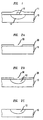
- FIG. 1 illustrates an example of an optical device in which the lower cladding is a region of densified, porous silicon formed in a semiconductor substrate.
- FIGS. 2A-2C illustrate an exemplary process sequence of the present invention.
- the present invention is directed to a method for forming a silica-based optical devices on a silicon substrate.
- silica-based optical devices There are a variety of silica-based optical devices. Such devices are well known to one skilled in the art and are not described in detail herein.
- the process of the present invention will be described in the context of fabricating a simple planar waveguide.
- the present process can be used to fabricate the full range of silica-based optical devices that are formed on a silicon substrate and require a lower cladding.
- FIG. 1 illustrates the general structure of a planar waveguide. It consists of three layers: core layer 10; upper clad layer 11; and lower clad 12. In one embodiment, all three layers are silica glass. The core layer is doped with phosphorus. In alternative embodiments, the core and upper cladding layers are plastic. The thickness of the individual layers is a matter of design choice. The appropriate thicknesses for a particular application are readily ascertained by one skilled in the art.
- the lower cladding is formed by depositing a patterned layer of material 20 (i.e. a mask) on the silicon substrate 15.
- the mask 20 defines the desired cladding region 30, which is the region of the substrate 15 that is exposed through the mask 20.
- the mask is formed using conventional lithographic techniques that are not described herein but are well known to one skilled in the art.
- FIG. 2A The structure depicted in FIG. 2A is placed in an annodization bath.
- the portions of the substrate 15 that are exposed to the anodization bath are converted to a porous silicon region 12 (the porous nature of region 12 is not illustrated in the FIGS.).
- the anodization proceeds isotropically, and a portion of the substrate underlying the mask 20 is converted to porous silicon. Consequently, the region of porous silicon 12 is larger than the mask opening 30.
- a porous silicon region with a depth of 15 ⁇ m will also extend 15 ⁇ m underneath the mask 20.
- mask materials are contemplated as suitable.
- suitable mask materials include photoresist, nitride, oxide, and carbide of silicon, polycrystalline silicon, and metals that are not soluble in HF solutions (e.g., gold, platinum etc.).
- HF solutions e.g., gold, platinum etc.
- Different masking materials have different etch-resistances for HF and thus should be chosen according to desired etch time and the process complexity.
- substantially fully oxidized means that conditions are selected to effect essentially complete oxidation of the porous silicon region.
- the conditions for substantially complete oxidation are readily ascertained by one skilled in the art. The selected conditions depend on the dimensions of the porous silicon region in the substrate. For example, complete oxidation of a 15 ⁇ m porous silicon region by heating the porous silicon region to 900°C in flowing, wet oxygen (100 percent humidity at 85°C) and holding the porous silicon region under these conditions for two hours.
- the substrate 15 is not oxidized to a substantial degree. To the extent that the substrate 15 is oxidized, such oxidized silicon is readily removed using conventional techniques. The thin layer of oxide that forms on the surface of substrate 15 is not shown in the Figure.
- the oxidized porous silicon region 12 is densified.
- the pores in the porous silicon region collapse and the porous silicon region is transformed into a dense glass region.
- the mechanism of densification is viscous flow. Therefore, the oxidized porous silicon must be heated to above its glass transition temperature (T g ) for this mechanism to occur.
- T g glass transition temperature
- Suitable conditions for densification are readily ascertained by one skilled in the art. For example, densification occurs when the oxidized porous silicon is subjected to elevated temperatures (e.g. 1150°C) in an atmosphere of wet oxygen for about two hours.
- the substrate 15 is not oxidized to a substantial degree. To the extent that the substrate 15 is oxidized, such oxidized silicon is readily removed using conventional techniques.
- the porous silicon is stabilized prior to oxidation and densification. Stabilization occurs using conditions that provide a few monolayers of oxide on the surface of the substrate 15. Suitable conditions are well known to one skilled in the art. Heating the wafers to a temperature of about 300°C in a dry oxygen atmosphere for about one hour stabilizes the porous silicon. The stabilization conditions are selected to prevent the porous silicon from oxidizing if it were stored at ambient temperature in an oxygen-containing atmosphere for some period of time before oxidation and densification.
- the core 10 is then formed on the cladding region 12 using conventional techniques not described herein.
- the upper cladding 11 is then formed over the core 10, again using conventional techniques.
- a pattern was delineated into the energy sensitive material.
- the pattern defined the lower cladding for a variety of optical devices, (i.e. straight waveguides, coupler and Mach-Zender devices).
- the smallest dimensions in the pattern were in the range of about 5 ⁇ m to about 7 ⁇ m.
- the same mask was used to define cores. Because anodization to form porous silicon is an isotropic process, the porous silicon region extended under the mask. Consequently, the dimensions of the porous silicon regions were larger than the mask dimensions (e.g the depth of the porous silicon region was 15 ⁇ m and the porous silicon region extended a distance of 15 ⁇ m under the mask.
- the pattern was delineated in the energy sensitive resist material using standard lithographic techniques.
- an image was transferred into the energy sensitive material by exposing the resist to patterned radiation.
- the image was then developed into a pattern by removing the portions of the energy sensitive material that were exposed to radiation. Removing portions of the energy sensitive material exposed the surface of the silicon substrate underlying those portions. The pattern of the removed portions corresponded to the mask pattern.
- the resist was baked at 150°C for 2 minutes. This was done to increase the stability of the resist during subsequent processing.
- the substrate with the patterned masking layer thereon was then subjected to a set of conditions that electrochemically etches silicon.
- the electrochemical cell used here was a standard double-tank cell. A cell of this type is described in Lang, W. et al., Sensors and Actuators A 51, pp. 31-36 (1995).
- the wafer was immersed in HF solution such that that both sides were immersed in solution and the wafer formed a barrier between two half-cells.
- Two platinum electrodes were located in each half-cell on both sides of the wafer. The electrical contact to the backside of the wafer was formed electrolytically, and the corresponding platinum electrode was the anode.
- the platinum electrode in the other half-cell was under cathodic potential.
- the two platinum electrodes were connected to the power supply that drives the current through the wafer.
- the front side of the wafer is anodically etched and porous silicon is formed at the areas not covered with the mask.
- the electrolyte was 25 weight percent ethanoic solution of hydrofluoric acid (HF).
- a current density of 150 mA/cm 2 provided an etch rate of 6.5 ⁇ m/min and a porosity of about 55%.
- the current was shut off and the substrate wafer was removed from the cell.
- the mask was stripped off of the substrate surface.
- the resist mask was removed in a bath of a standard organic resist stripper.
- the substrate was heated to 300°C and held for two hours in an oxygen atmosphere.
- the substrate was heated to 900°C in an atmosphere of wet (100 percent humidity at 85°C) oxygen (flowing) and held there for two hours hour.
- the porous silicon was oxidized but did not measurably expand in the vertical direction, i.e., it remained planar with the substrate surface. Because the porous silicon surface did not increase or decrease in elevation compared to the rest of the substrate surface, further processing was complicated by the presence of the porous silicon region.
- the porous silicon was then densified by heating the wafer to 1150°C in an atmosphere of wet flowing oxygen. The wafer was held in this atmosphere for two hours. The wafer was then cooled to room temperature at a rate of about 100°C per hour.
- a layer of doped glass material was then deposited on the densified porous silicon region.
- the doped glass was silica doped with phosphorus (seven weight percent).
- the doped glass material was deposited using LPCVD. The dopants were introduced into the glass in situ.
- the core of the optical device was then formed by patterning the doped glass layer.
- An etch mask layer was formed over the doped glass layer.
- the etch mask layer was then patterned, so that the remaining portion of the etch mask layer defined the core of the optical device being formed.
- the doped glass material was then etched using reactive ion etching (RIE). After etching, the portion of the doped glass layer that remains is the core of the optical device. The remaining portion of the RIE etch mask was then removed.
- RIE reactive ion etching
- silica glass is formed over the substrate.
- the layer of silica glass was deposited using LPCVD from tetraethyl orthosilicate (TEOS) precursors.
- TEOS tetraethyl orthosilicate
- the glass composition silica doped with boron (five weight percent) and phosphorus (2 weight percent).
- the completed devices were evaluated for their performance, which was normal.
- the total insertion loss for a straight waveguide (6 cm in length) was about 1.2 dB. Consequently, the propagation loss for the waveguide was about 0.2 dB/cm.
- the propagation loss was actually lower, because, out of the total 1.2 dB, about 0.4 dB to about 0.5 dB were coupling losses between the waveguide and the input and output fibers. Therefore, the propagation loss of the waveguide was actually about 0.15 dB/cm.
Landscapes
- Physics & Mathematics (AREA)
- Engineering & Computer Science (AREA)
- Microelectronics & Electronic Packaging (AREA)
- General Physics & Mathematics (AREA)
- Optics & Photonics (AREA)
- Optical Integrated Circuits (AREA)
Abstract
Description
Claims (9)
- A method for fabricating an optical device comprising:forming a region of porous silicon in a silicon substrate:oxidizing the region of porous silicon;densifying the region of porous silicon; andforming an active portion of an optical device on the densified porous silicon
- The method of claim 1 wherein the region of porous silicon is formed by anodization.
- The method of claim 2 wherein the region of porous silicon is defined by a mask formed on the silicon substrate prior to anodization.
- The method of claim 1 wherein the density of the porous silicon is about forty-four percent.
- The method of claim 1 wherein the region of porous silicon is oxidized by heating the substrate to a temperature of about 850°C to about 1150°C in an oxygen-containing atmosphere.
- The method of claim 5 wherein the duration of the oxidizing step is sufficient to substantially completely oxidize the porous silicon region.
- The method of claim 1 wherein the oxidized porous silicon is densified using conditions that convert the oxidized porous silicon to silica.
- The process of claim 7 wherein the porous silicon is densified by heating the substrate in an oxygen-containing atmosphere.
- The process of claim 1 further comprising stabilizing the porous silicon region prior to the oxidizing step.
Applications Claiming Priority (2)
| Application Number | Priority Date | Filing Date | Title |
|---|---|---|---|
| US451433 | 1999-11-30 | ||
| US09/451,433 US6312581B1 (en) | 1999-11-30 | 1999-11-30 | Process for fabricating an optical device |
Publications (2)
| Publication Number | Publication Date |
|---|---|
| EP1107026A2 true EP1107026A2 (en) | 2001-06-13 |
| EP1107026A3 EP1107026A3 (en) | 2003-03-05 |
Family
ID=23792193
Family Applications (1)
| Application Number | Title | Priority Date | Filing Date |
|---|---|---|---|
| EP00310296A Withdrawn EP1107026A3 (en) | 1999-11-30 | 2000-11-20 | A process for fabricating a silica-based optical device on a silicon substrate |
Country Status (5)
| Country | Link |
|---|---|
| US (1) | US6312581B1 (en) |
| EP (1) | EP1107026A3 (en) |
| JP (1) | JP5137278B2 (en) |
| CN (1) | CN1298110A (en) |
| CA (1) | CA2323683C (en) |
Families Citing this family (13)
| Publication number | Priority date | Publication date | Assignee | Title |
|---|---|---|---|---|
| JP2001324631A (en) * | 2000-05-12 | 2001-11-22 | Nec Corp | Substrate, optical fiber connection end member, optical element housing member, optical module and substrate manufacturing method |
| WO2002005349A1 (en) * | 2000-07-12 | 2002-01-17 | California Institute Of Technology | Electrical passivation of silicon-containing surfaces using organic layers |
| US6603915B2 (en) * | 2001-02-05 | 2003-08-05 | Fujitsu Limited | Interposer and method for producing a light-guiding structure |
| GB2374457A (en) * | 2001-04-09 | 2002-10-16 | Bookham Technology Plc | Hybridised Fibre Amplifier/Waveguide Structures |
| US20030002771A1 (en) * | 2001-06-01 | 2003-01-02 | Jds Uniphase Corporation | Integrated optical amplifier |
| US6946238B2 (en) * | 2001-06-29 | 2005-09-20 | 3M Innovative Properties Company | Process for fabrication of optical waveguides |
| US6873638B2 (en) | 2001-06-29 | 2005-03-29 | 3M Innovative Properties Company | Laser diode chip with waveguide |
| US6832034B2 (en) * | 2002-06-21 | 2004-12-14 | 3M Innovative Properties Company | Optical waveguide |
| WO2006035893A1 (en) * | 2004-09-30 | 2006-04-06 | Hamamatsu Photonics K.K. | Silicon substrate processing method |
| US7394961B2 (en) * | 2005-10-13 | 2008-07-01 | Pavel Kornilovich | Waveguide having low index substrate |
| US8290325B2 (en) * | 2008-06-30 | 2012-10-16 | Intel Corporation | Waveguide photodetector device and manufacturing method thereof |
| US9470710B2 (en) * | 2013-02-27 | 2016-10-18 | Texas Instruments Incorporated | Capacitive MEMS sensor devices |
| US9520811B2 (en) | 2013-02-27 | 2016-12-13 | Texas Instruments Incorporated | Capacitive micromachined ultrasonic transducer (CMUT) device with through-substrate via (TSV) |
Family Cites Families (7)
| Publication number | Priority date | Publication date | Assignee | Title |
|---|---|---|---|---|
| US4016017A (en) * | 1975-11-28 | 1977-04-05 | International Business Machines Corporation | Integrated circuit isolation structure and method for producing the isolation structure |
| US4532700A (en) * | 1984-04-27 | 1985-08-06 | International Business Machines Corporation | Method of manufacturing semiconductor structures having an oxidized porous silicon isolation layer |
| US5391269A (en) | 1993-06-29 | 1995-02-21 | At&T Corp. | Method of making an article comprising a silicon body |
| US5448586A (en) | 1993-09-20 | 1995-09-05 | At&T Corp. | Pumping arrangements for arrays of planar optical devices |
| US5907791A (en) | 1996-04-25 | 1999-05-25 | Lucent Technologies Inc. | Method of making semiconductor devices by patterning a wafer having a non-planar surface |
| DE19755416C1 (en) * | 1997-12-12 | 1999-06-10 | Bosch Gmbh Robert | Producing a light guide in a silver cation exchanged silicon dioxide layer on a silicon substrate |
| JPH11194221A (en) * | 1998-01-07 | 1999-07-21 | Oki Electric Ind Co Ltd | Method of forming optical waveguide and optical waveguide device |
-
1999
- 1999-11-30 US US09/451,433 patent/US6312581B1/en not_active Expired - Lifetime
-
2000
- 2000-10-18 CA CA002323683A patent/CA2323683C/en not_active Expired - Fee Related
- 2000-11-13 JP JP2000344642A patent/JP5137278B2/en not_active Expired - Fee Related
- 2000-11-20 EP EP00310296A patent/EP1107026A3/en not_active Withdrawn
- 2000-11-29 CN CN00134267A patent/CN1298110A/en active Pending
Also Published As
| Publication number | Publication date |
|---|---|
| JP5137278B2 (en) | 2013-02-06 |
| CA2323683C (en) | 2006-06-06 |
| US6312581B1 (en) | 2001-11-06 |
| CA2323683A1 (en) | 2001-05-30 |
| EP1107026A3 (en) | 2003-03-05 |
| JP2001166168A (en) | 2001-06-22 |
| CN1298110A (en) | 2001-06-06 |
Similar Documents
| Publication | Publication Date | Title |
|---|---|---|
| US6312581B1 (en) | Process for fabricating an optical device | |
| US6890450B2 (en) | Method of providing optical quality silicon surface | |
| US6850683B2 (en) | Low-loss waveguide and method of making same | |
| CA2507533A1 (en) | Process for fabrication of optical waveguides | |
| US5342478A (en) | Self-aligned V-grooves and waveguides | |
| CN114895401B (en) | Silicon photon chip optical coupling structure and manufacturing method thereof | |
| US6370307B1 (en) | Optical device formed on a substrate with thermal isolation regions formed therein | |
| KR100377186B1 (en) | Fabrication method of polymeric arrayed waveguide grating wavelength multiplexer /demultiplexer | |
| CN215067652U (en) | Channel-type planar waveguide amplifier, optical device and optical equipment | |
| JP2004515815A (en) | Waveguide including channel on optical substrate | |
| JP4681644B2 (en) | Optical waveguide fabrication method | |
| US20040091225A1 (en) | Optically active waveguide device comprising a channel on an optical substrate | |
| CN1326104A (en) | Mechanically modulated WDM transmitting and receiving module | |
| US6631235B1 (en) | Planar lightwave circuit platform and method for manufacturing the same | |
| JP3559528B2 (en) | Opto-electric circuit board | |
| Jalali | Silicon-on-insulator photonic integrated circuit (SOI-PIC) technology | |
| KR100367087B1 (en) | Method of manufacturing planar optical waveguides through negative etching | |
| CN222259620U (en) | Selective epitaxial silicon-based ridge optical waveguide | |
| KR100650820B1 (en) | Method for producing planar lightwave circuit device | |
| JPH1152175A (en) | Optical integrated circuit substrate and method of manufacturing the same | |
| CN110908037A (en) | Optical waveguide and method for manufacturing the same | |
| JPH09292540A (en) | Manufacturing method of optical waveguide device | |
| WO1996041219A1 (en) | A method of making integrated optical waveguides, and an optical unit having integrated optical waveguides | |
| WO2026030587A1 (en) | Selective porosification for volumetric optical devices | |
| JP2000081525A (en) | Planar lightwave circuit platform and fabrication method thereof |
Legal Events
| Date | Code | Title | Description |
|---|---|---|---|
| PUAI | Public reference made under article 153(3) epc to a published international application that has entered the european phase |
Free format text: ORIGINAL CODE: 0009012 |
|
| AK | Designated contracting states |
Kind code of ref document: A2 Designated state(s): AT BE CH CY DE DK ES FI FR GB GR IE IT LI LU MC NL PT SE TR |
|
| AX | Request for extension of the european patent |
Free format text: AL;LT;LV;MK;RO;SI |
|
| RAP1 | Party data changed (applicant data changed or rights of an application transferred) |
Owner name: AGERE SYSTEMS OPTOELECTRONICS GUARDIAN CORPORATION |
|
| PUAL | Search report despatched |
Free format text: ORIGINAL CODE: 0009013 |
|
| AK | Designated contracting states |
Kind code of ref document: A3 Designated state(s): AT BE CH CY DE DK ES FI FR GB GR IE IT LI LU MC NL PT SE TR Designated state(s): AT BE CH CY DE DK ES FI FR GB GR IE IT LI LU MC NL PT SE TR |
|
| AX | Request for extension of the european patent |
Extension state: AL LT LV MK RO SI |
|
| 17P | Request for examination filed |
Effective date: 20030812 |
|
| AKX | Designation fees paid |
Designated state(s): DE FR GB |
|
| 17Q | First examination report despatched |
Effective date: 20031119 |
|
| STAA | Information on the status of an ep patent application or granted ep patent |
Free format text: STATUS: THE APPLICATION IS DEEMED TO BE WITHDRAWN |
|
| 18D | Application deemed to be withdrawn |
Effective date: 20050301 |