EP1106994A2 - Inspection apparatus and method - Google Patents
Inspection apparatus and method Download PDFInfo
- Publication number
- EP1106994A2 EP1106994A2 EP00125362A EP00125362A EP1106994A2 EP 1106994 A2 EP1106994 A2 EP 1106994A2 EP 00125362 A EP00125362 A EP 00125362A EP 00125362 A EP00125362 A EP 00125362A EP 1106994 A2 EP1106994 A2 EP 1106994A2
- Authority
- EP
- European Patent Office
- Prior art keywords
- resist pattern
- image
- illumination light
- image pickup
- illumination
- Prior art date
- Legal status (The legal status is an assumption and is not a legal conclusion. Google has not performed a legal analysis and makes no representation as to the accuracy of the status listed.)
- Granted
Links
Images



Classifications
-
- G—PHYSICS
- G01—MEASURING; TESTING
- G01N—INVESTIGATING OR ANALYSING MATERIALS BY DETERMINING THEIR CHEMICAL OR PHYSICAL PROPERTIES
- G01N21/00—Investigating or analysing materials by the use of optical means, i.e. using sub-millimetre waves, infrared, visible or ultraviolet light
- G01N21/84—Systems specially adapted for particular applications
- G01N21/88—Investigating the presence of flaws or contamination
- G01N21/95—Investigating the presence of flaws or contamination characterised by the material or shape of the object to be examined
- G01N21/956—Inspecting patterns on the surface of objects
-
- H—ELECTRICITY
- H10—SEMICONDUCTOR DEVICES; ELECTRIC SOLID-STATE DEVICES NOT OTHERWISE PROVIDED FOR
- H10P—GENERIC PROCESSES OR APPARATUS FOR THE MANUFACTURE OR TREATMENT OF DEVICES COVERED BY CLASS H10
- H10P74/00—Testing or measuring during manufacture or treatment of wafers, substrates or devices
Definitions
- the present invention relates to an inspection apparatus and an inspection method suitable for inspecting the state of a resist pattern formed on a semiconductor wafer in a lithography step in semiconductor process.
- inspection apparatuses having a high resolution are those using a scanning electron microscope (SEM), an atomic force microscope (AFM), and the like.
- SEM scanning electron microscope
- AFM atomic force microscope
- these scanning electron microscopes and atomic force microscopes require vacuum in inspection, and are therefore inconvenient for handling. In addition, it takes much time to inspection entirely a semiconductor device.
- an inspection apparatus using an optical microscope is advantageous in that inspection can be carried out undestructively without necessitating vacuum or contact.
- a ultraviolet solid laser apparatus which performs wave-conversion on a YAG laser or the like with use of non-linear optical crystal thereby to emit laser light having a wavelength of a ultraviolet range. If this ultraviolet solid laser apparatus is used as an illumination light source and if an optical system is constructed by using an objective lens having a high NA, even an optical microscope can attain a resolution close to that of a scanning electronic microscope. Hence, expectation is much devoted to the optical microscope.
- This resist pattern is formed in a manner that resist material coated on a semiconductor wafer is exposed by an exposure apparatus and developed, in accordance with a pattern to be formed.
- a resist pattern as described above is inspected by an inspection apparatus which inspects an inspection target by picking up an image of the inspection target by an image pickup element such as a CCD (charge-coupled device) camera or the like, with an ultraviolet solid laser apparatus used as an illumination light source.
- an image pickup element such as a CCD (charge-coupled device) camera or the like
- an ultraviolet solid laser apparatus used as an illumination light source.
- the wavelength of illumination light is close to the wavelength of a light source of an exposure apparatus. Therefore, the resist pattern to be detected may contract in response to the illumination light if the irradiation light amount of the illumination light is large.
- an anti-reflection film is normally provided in the vicinity of the resist pattern in order to prevent abnormal exposure due to reflection during exposure, the absorption rate of this anti-reflection film changes thereby influencing harmfully the inspection of the resist pattern, if the irradiation light amount of the illumination light is large.
- the noise component of the image pickup element is large relatively to the obtained signal component, so that the resist pattern cannot be inspected with good accuracy in some cases.
- the present invention has been proposed in view of the situation described above and has an object of providing an inspection apparatus and an inspection method capable of inspect a resist pattern accurately and properly by irradiating illumination light at a proper irradiation light amount on a resist pattern to be inspected.
- An inspection apparatus comprises: illumination means for irradiating a resist pattern as an inspection target with illumination light having a wavelength of 355 nm or less within an ultraviolet range; image pickup means for picking up an image of the resist pattern illuminated by the illumination means; an imaging optical system for forming an image of the resist pattern illuminated by the illumination means; and image processing means for processing the image of the resist pattern picked up by the image pickup means.
- the imaging magnification of the imaging optical system is set such that the image resolution of the image pickup means falls in a range from 10 nm to 30 nm on the resist pattern.
- the "image resolution” means a value expressing how large area on the resist pattern as an inspection target one minimum image pickup unit (one pixel) of the image pickup means corresponds to.
- the imaging magnification is set such that the image resolution of the image pickup means falls in a range from 10 nm to 30 nm.
- the illumination means irradiates the resist pattern with the illumination light at an irradiation light amount within a range from 0.5 mJ/cm 2 to an irradiation threshold value at which the resist pattern is not caused to contract or an irradiation threshold value at which an absorption rate of an anti-reflection film provided near the resist pattern is not caused to change, every time when the image pickup means picks up an image.
- a resist pattern as an inspection target is illuminated with illumination light having a wavelength of 355 nm within an ultraviolet range. Further, an image of the resist pattern illuminated with the illumination light having a wavelength within the ultraviolet range is guided to and formed by the image pickup means. At this time, the image resolution of the image pickup means corresponds to an area ranging from 10 nm to 30 nm.
- the image of the resist pattern picked up by the image pickup means is taken in and processed by the image processing means.
- the image of the resist pattern thus processed by the image processing means is an image of the resist pattern illuminated with the illumination light having a wavelength within an ultraviolet range, which is light having a very short wavelength. Therefore, the state of the resist pattern can be inspected very accurately by analyzing the image of the resist pattern processed by the image processing means.
- the illumination means irradiates illumination light on the resist pattern at an irradiation light amount within the range described above, every time when the image pickup means picks up one image. Therefore, the noise component of the image pickup element can be reduced relatively to the signal component, so that the inspection accuracy can be improved. In addition, contraction of the resist pattern and change of characteristics of the anti-reflection film can be prevented effectively so that inspection of the resist pattern can be carried out properly.
- the resist pattern is not irradiated with an irradiation light amount equal to or higher than 0.5 mJ/cm 2 every time when the image pickup means picks up an image, the ratio of the noise component to the signal component becomes too high to inspect accurately the resist pattern, in an inspection apparatus in which the image resolution of the image pickup means on the resist pattern is set within a range from 10 nm to 30 nm.
- the resist pattern causes contraction. If it exceeds an irradiation threshold value at which the absorption rate of the resist pattern is not caused to change, the absorption rate of the resist pattern changes. In any cases, proper inspection is hindered.
- the illumination means irradiates the resist pattern with the illumination light at the irradiation light amount within the range from 0.5 mJ/cm 2 to the irradiation threshold value at which the resist pattern is not caused to contract or the irradiation threshold value at which the absorption rate of the anti-reflection film provided near the resist pattern is not caused to change, every time when the image pickup means picks up an image. Therefore, the resist pattern can be inspected accurately and properly.
- illumination light is irradiated on a resist pattern as an inspection target with illumination light, an image of the resist pattern thus illuminated is picked up by image pickup means, and the image of the resist pattern picked up by the image pickup means is processed and analyzed, thereby to inspect a state of the resist pattern.
- the resist pattern is irradiated with illumination light having a wavelength of 355 nm or less within an ultraviolet range at an irradiation light amount within a range from 0.5 mJ/cm 2 to an irradiation threshold value at which the resist pattern is not caused to contract or an irradiation threshold value at which an absorption rate of an anti-reflection film provided near the resist pattern is not caused to change, every time when the image pickup means picks up an image, and the image of the resist pattern illuminated with the illumination light is formed on the image pickup means with use of an image optical system in which an imaging magnification is set such that an image resolution of the image pickup means falls within a range from 10 nm to 30 nm.
- the image of the resist pattern illuminated with the illumination light having a wavelength within an ultraviolet range, which is light having a very short wavelength is processed and analyzed thereby to inspect the state of the resist pattern. Therefore, the state of the resist pattern can be inspected very accurately.
- the illumination means irradiates the resist pattern with the illumination light at the irradiation light amount within the range from 0.5 mJ/cm 2 to the irradiation threshold value at which the resist pattern is not caused to contract or the irradiation threshold value at which the absorption rate of the anti-reflection film provided near the resist pattern is not caused to change. Therefore, while maintaining a sufficient signal component in relation to the noise component of the image pickup element, contraction of the resist pattern and change of characteristics of the anti-reflection film can be restricted effectively so that the resist pattern can be inspected properly.
- a resist pattern having a micro structure can be inspected properly and accurately, without causing contraction of the resist pattern or change of characteristics of an anti-reflection film provided near the resist pattern.
- a resist pattern formed on the semiconductor wafer or the like is illuminated with illumination light having a wavelength within an ultraviolet range, to pick up an image.
- the image thus picked up is subjected to processing and analysis, to detect edge positions of a resist pattern, so that the line width is managed or so.
- the resist pattern formed on the semiconductor wafer has become more micro as the integration of the semiconductor integrated circuit or the like has been improved.
- To inspect optically this micro resist pattern with high accuracy it is effective to use light having a short wavelength as illumination light.
- the present invention uses light having a short wavelength of 355 nm or less within an ultraviolet range as illumination light.
- an anti-reflection film by which reflection during exposure and formation of a resist pattern is prevented to form the resist pattern into an appropriate shape, is provided as an upper or lower layer of the resist pattern.
- the absorption rate of the anti-reflection film is changed if the irradiation light amount is so large so as to exceed a predetermined value. As a result, the intensity of light reflected by the anti-reflection film is suddenly increased as shown in FIG. 1.
- the picked-up image of the resist pattern changes in accordance with the condition of the anti-reflection film, so that harmful influences can be made on the inspection accuracy. Therefore, in case of using light having a wavelength within an ultraviolet range as illumination light, it is important to illuminate the resist pattern at an irradiation light amount which does not cause the anti-reflection film to change its absorption rate.
- the irradiation light amount of the illumination light for picking up an image must be set to be equal to or less than an irradiation threshold value at which a resist pattern is not caused to contract or an irradiation threshold value at which an anti-reflection film is not caused to change its absorption rate, in order to inspect a resist pattern, using light having a wavelength of 355 nm or less within an ultraviolet range as illumination light.
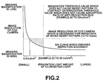
- the irradiation light amount of the illumination light for picking up an image should be set preferably to 20 to 30 mJ/cm 2 or less or more preferably to about 1 mJ/cm 2 .
- a problem lies in noise of the image pickup element such as a CCD camera or the like which picks up an image. That is, in the weak light inspection, the light amount which enters into the CCD camera is small, so that the ratio of the noise component increases relatively to the signal component. This noise component becomes a factor which deteriorates the inspection accuracy.
- the noise of the CCD camera includes shot noise electronically generated when photoelectrically converting light which has entered into the CCD camera, read noise generated when transferring image data picked up by the CCD camera to an image processing means of an image processing computer, heat noise, and the like.
- the read noise and heat noise of the CCD camera can be effectively restricted by cooling the chip of the CCD camera.
- read noise and heat noise of the CCD camera can be greatly reduced by the chip of the CCD camera to 5 °C or less by use of a Peltier element, compared with the case of using it at an ordinary temperature.
- the CCD camera is constructed with use of a CCD chip which shows high quantum efficiency within an ultraviolet range, and this CCD camera is used as an image pickup element. In this manner, it is possible to reduce the shot noise ratio with respect to the amount of the light received by the image pickup element.
- the quantum efficiency of a CCD camera means the ratio of the number of generated electrons to the number of incident photons, including the surface transmittance, internal absorption, and photoelectric conversion rate, and the like.
- the shot noise ratio must be lowered to a constant level or less by illuminating the resist pattern with a constant irradiation light amount or more so that an amount of light enough to maintain the inspection accuracy enters into the CCD camera.
- the number of photons that enter into one minimum image pickup unit (1 pixel) of a CCD camera is not determined uniformly by the irradiation light amount of the illumination light but also depends on the imaging magnification of an imaging optical system for forming an image of a resist pattern illuminated with illumination light on the CCD camera. That is, if the irradiation light amount of the illumination light is constant, the number of photons that enter into one pixel of the CCD camera increases and the ratio of the signal component to the shot noise also increases as the imaging magnification of the imaging optical system is lower.
- the imaging magnification of the imaging optical system is a parameter which determines the image resolution. If the imaging magnification of the imaging optical system is too low, an area on the resist pattern, which corresponds to one example, becomes so large that it is difficult to inspect accurately a micro structure.
- the imaging magnification should preferably be set such that the image resolution of the CCD camera is within a range from 10 nm to 30 nm or is more preferably about 24 nm.
- the resist pattern must be illuminated at an irradiation light amount of about 0.5 mJ/cm 2 or more, as shown in FIG. 2, in order to maintain an inspection accuracy by increasing the ratio of the signal component to the shot noise.
- the present invention is arranged as follows. That is, the imaging magnification is set such that the image resolution of the CCD camera is within a range from 10 nm to 30 nm on the resist pattern, and the irradiation light amount of the illumination light irradiated on the resist pattern is set within a range from 0.5 mJ/cm 2 to an irradiation threshold value at which the resist pattern is not caused to contract or an irradiation threshold value at which an anti-reflection film provided near the resist pattern is not caused to change (the area indicated by hatching in FIG. 2). In this manner, a micro resist pattern can be inspected properly and accurately.
- FIG. 3 shows a structural example of an inspection apparatus to which the present invention is applied.
- the inspection apparatus 1 shown in FIG. 3 serves to inspect the state of a resist pattern formed on a semiconductor wafer with an anti-reflection film inserted therebetween.
- the inspection apparatus comprises a movable stage 2 which supports a semiconductor wafer 100 where a resist pattern is formed, an ultraviolet solid laser device 3 which emits illumination light having a wavelength within an ultraviolet range, an acoustic optics modulator (AOM) 4 which acoustically modulates the illumination light emitted from the ultraviolet solid laser device 3, an ultraviolet CCD camera 5 which picks up an image of the resist pattern illuminated with the illumination light, an imaging optical system 6 which forms an image of the resist pattern illuminated with the illumination light, on the CCD car-era 5, an image processing computer 7 which processes the image of the resist pattern picked up by the CCD camera 5, and a control computer 8 which controls operation of the entire inspection apparatus 1.
- AOM acoustic optics modulator
- the movable stage 2 comprises, for example, X- and Y-stages for moving the semiconductor wafer 100 set on the movable stage 2 in the horizontal direction, a Z-stage for moving the semiconductor wafer 100 in the vertical direction, a è-stage for rotating the semiconductor wafer 100, and a suction plate for suctioning the semiconductor wafer 100 to fix it to the movable stage 2. Further, the movable stage 2 operates the other stages described above under control from the control computer 8, thereby to move the portion to be inspected of the semiconductor wafer 100 to a predetermined inspection position.
- the ultraviolet solid laser device 3 performs wavelength-conversion on a solid laser such as a YAG laser or the like with use of a non-linear optical crystal, thereby to emit a deep ultraviolet (DUV) laser beam having a wavelength of about 266 nm, for example.
- a solid laser such as a YAG laser or the like with use of a non-linear optical crystal, thereby to emit a deep ultraviolet (DUV) laser beam having a wavelength of about 266 nm, for example.
- DUV deep ultraviolet
- the inspection ability of the inspection apparatus depends on the wavelength of the illumination light to be irradiated on an inspection target. Illumination light with a shorter wavelength of the illumination light enables inspection of a more micro pattern.
- the inspection apparatus 1 uses an ultraviolet solid laser apparatus 3 as a light source of the illumination light, so that the semiconductor wafer 100 can be illuminated with a deep ultraviolet laser beam having a short wavelength. It is therefore possible to inspect a micro pattern.
- the ultraviolet solid laser device 3 itself has a small size and requires no water-cooling. Thus, the device 3 provides easy handling, and is suitable for a light source of illumination light. Note that a deep ultraviolet laser beam having a wavelength of 266 nm can be obtained as a quadruple wave of a YAG laser beam.
- the acoustic optical modulator 4 is an optical modulator using an acoustic optical effect.
- the intensity of primary diffraction light in Bragg diffraction or Debye sheath effect is substantially proportional to the ultrasonic power. Therefore, the intensity of the primary diffraction light can be electrically adjusted by controlling an RF signal inputted to the acoustic optical modulator 4 to modulate the ultrasonic power.
- illumination light emitted from the ultraviolet solid laser device 3 is let enter into the acoustic optical modulator 4, and the primary diffraction light diffracted by this acoustic optical modulator 4 is irradiated as illumination light on a resist pattern as an inspection target.
- the RF signal inputted to the acoustic optical modulator 4 is controlled by a control computer 8 thereby to adjust the irradiation light amount of the illumination light to be irradiated on the resist pattern.
- the ultraviolet CCD camera 5 is, for example, a CCD camera constructed such that a high sensitivity can be attained with respect to ultraviolet light. For example, a quantum efficiency of about 30 % or more is obtained with respect to a deep ultraviolet laser beam having a wavelength of about 266 nm. Also, the ultraviolet CCD camera 5 is structured such that the CCD chip is cooled to about 5 °C by a Peltier element. Thus, it is possible to reduce greatly read noise and heat noise which are caused when image data picked up by the ultraviolet CCD camera 5 is transferred to the image processing computer 7.
- the imaging optical system 6 comprises an ultraviolet objective lens 11 and an imaging lens 12 and serves to form an image of a resist pattern, which is illuminated with illumination light, at a predetermined imaging magnification on the ultraviolet CCD camera 5.
- the imaging magnification of the imaging optical system 6 is set such that the image resolution of the ultraviolet CCD camera 5 is within a range from 10 nm to 30 nm on the resist pattern being inspected, i.e., an area of 10 to 30 nm on the resist pattern corresponds to one pixel of the ultraviolet CCD camera 5.
- the semiconductor wafer 100 on which a resist pattern 102 is formed with an anti-reflection film 101 inserted therebetween is set on the movable table 2. Further, the movable table 2 is driven under control of the control computer 7, and motion of the semiconductor wafer 100 is controlled, so that the portion to be inspected of the resist pattern 102 is positioned at a predetermined inspection position.
- the ultraviolet solid laser device 3 is driven under control from the control computer 7, so as to emit a deep ultraviolet laser beam having a wavelength of about 266 nm from the laser device 3, for example.
- the ultraviolet laser beam emitted from the ultraviolet solid laser device 3 is incident to the acoustic optical modulator 4.
- the acoustic optical modulator 4 modulates incident light under control from the control computer 8. Specifically, an RF signal inputted to the acoustic optical modulator 4 from the control computer 8 is controlled thereby to adjust the intensity of primary diffraction light of the deep ultraviolet laser beam which is transmitted through the acoustic optical modulator 4.
- the primary diffraction light is irradiated as illumination light onto the resist pattern 102 as an inspection target.
- illumination light is irradiated on the resist pattern 102 as an inspection target at an irradiation light amount within a range from 0.5 mJ/cm 2 to an irradiation threshold value at which the resist pattern 102 is not caused to contract or an irradiation threshold value at which the anti-reflection film 101 is not caused to change its absorption rate, every time when the ultraviolet CCD camera 5 picks up an image.
- the irradiation light amount of the illumination light to be irradiated on the resist pattern 102 as an inspection target is controlled electrically with use of the acoustic optical modulator 4 controlled by the control computer 8. Therefore, the irradiation light amount of the illumination light can be controlled properly, simply, and easily. Also, in this inspection apparatus 1, illumination light can be irradiated on the resist pattern 102 as an inspection target, for example, in synchronization with the shutter of the ultraviolet CCD camera 5. Irradiation of illumination light can be performed efficiently.
- the primary diffraction light (illumination light) which has been transmitted through the acoustic optical modulator 4 is introduced to the part of the optical system by an ultraviolet optical fiber 13. Further this illumination light is transmitted through a lens 14 and enters into a beam splitter 15. The illumination light reflected by the beam splitter 15 is irradiated on the resist pattern 102 of the semiconductor wafer 100 set on the movable table 2. In this manner, the resist pattern 102 as an inspection target is illuminated with the illumination light which is a deep ultraviolet laser beam whose light amount is controlled.
- the reflection light from the resist pattern 102 illuminated by the illumination light is transmitted through the ultraviolet objective lens 11 and enters into the beam splitter 15. Further, the reflection light from the resist pattern 102, which has been transmitted through the beam splitter, enters into the ultraviolet CCD camera 5 through an imaging lens 12. In this manner, an image of the resist pattern, which is enlarged by the ultraviolet objective lens 11 as shown in FIG. 5, is picked up by the ultraviolet CCD camera 5.
- a lens having a high numerical aperture NA of about 0.9 is used as the ultraviolet objective lens 11.
- a deep ultraviolet laser beam having a short wavelength is used as the illumination light
- a lens having a high numerical aperture is used as the ultraviolet objective lens 11, thus enabling inspection of a more micro pattern.
- a countermeasure capable of reducing the aberration with respect to an ultraviolet light having a wavelength of about 266 nm is adopted in the ultraviolet objective lens 11.
- the ultraviolet objective lens 11 is movable in the direction in which the lens comes closer to the resist pattern 102 as an inspection target, by a focus adjust mechanism 16 driven under control from the control computer 8. Therefore, the lens is arranged such that focus adjustment can be achieved by the control from the control computer 8.
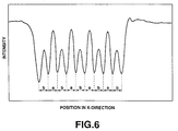
- the image of the resist pattern 102 picked up by the ultraviolet CCD camera 5 is taken in by the image processing computer 7. Further, the image processing computer 7 processes the image of the take-in resist pattern 102 thereby to prepare an intensity profile of light, as shown in FIG. 6.
- the intensity profile shown in FIG. 6 is obtained when illumination light diffracted by the resist pattern 102 constructed by concaves and convexes causes interference near gaps therebetween.
- This profile corresponds to the concaves and convexes of the resist pattern 102. That is, the large crests appearing on the intensity profile (e.g., the portions indicated at the reference a in FIG. 6) correspond to concave portions of the resist pattern 102, and portions each appearing between two large crests (e.g., the portions indicated at the reference b in FIG. 6) on the intensity profile correspond to convex portions of the resist pattern 102. Also on the intensity profile, a small crest appears between every two large crests, and a peak as a trough appears between every adjacent small and large crests. The peaks as troughs correspond to boundary portions between concave and convex portions (hereinafter called pattern edges).
- the inspection apparatus 1 to which the present invention is applied it is thus possible to obtain an intensity profile on which peaks as troughs appear in correspondence with pattern edges of the resist pattern 102. It is therefore possible to measure the width (line width) of each convex portion of the resist pattern 102 from the intensity profile. That is, on the intensity profile obtained by the inspection apparatus 1, the portion sandwiched between two peaks as troughs corresponds to the width of a convex portion. Accordingly, a line width of the resist pattern 102 can be measured by obtaining the distance between two peaks as troughs.
- the part of a trough of the intensity profile is fitted to a quadric function. Further, an extreme of the quadric function is detected as a peak of a trough portion. In this manner, it is possible to obtain the positions of peaks of trough portions, which correspond to pattern edges of the resist pattern 102, with a high accuracy equivalent to the pixel size of the ultraviolet CCD camera 5 or less.
- a distance between adjacent peaks of two troughs is measured.
- the distance between peaks of two troughs corresponds a line width of the resist pattern 102.
- An obtained distance between peaks of two troughs i.e., an observation value of a line width of the resist pattern 102
- an actual value absolute value
- the absolute value can be obtained by correcting an observation value of a line width of the resist pattern 102 if the ratio of an observation value to an absolute value of a line width of the resist pattern 102 is previously obtained with use of a scanning electron microscope (SEM) or the like.
- a line width of the resist pattern 102 can be measured accurately in the order of nano-meter if a line width of the resist pattern 102 is obtained from an intensity profile prepared by the image processing computer 7.
- the line width of the resist pattern 102 changes, the change of the line width can be detected with excellent accuracy.
- a pattern of a semiconductor integrated circuit includes a layered structure
- positional dislocations of layering of patterns including the layered structure can be detected accurately by specifying pattern edges of a resist pattern corresponding to a lower pattern and pattern edges of a resist pattern corresponding to an upper pattern respectively, and by inspecting variants of these pattern edges.
- the line width can be measured more accurately by averaging inspection results of a plurality of lines. That is, there is a limit to reduction of shot noise caused by the ultraviolet CCD camera 5, and the shot noise therefore causes variants of the measurement accuracy between lines, in some cases.
- inspection results of a plurality of lines are averaged and the average value is set as the line width of the resist pattern 102, the variants of the measurement accuracy between the lines can be averaged, so that the line width of the resist pattern 102 can be obtained more accurately.
- this inspection apparatus 1 uses ultraviolet light as illumination light, it is difficult to make focus adjustment such that the distance between the ultraviolet objective lens 11 and the resist pattern 102 as an inspection target accurately corresponds to the focal length of the ultraviolet objective lens 11. Also, in this inspection apparatus 1, there is a case that the resist pattern 102 is inspected much more accurately if the resist pattern 102 is observed in an off-focus state slightly shifted from an on-focus state, depending on the size of the resist pattern 102 to be inspected.
- the inspection apparatus 1 coarse focus adjustment is carried out by the focus adjustment mechanism 16 described above. Thereafter, while the Z-stage of the movable stage 2 is moved finely to change slightly the position of the resist pattern 102 to be inspected, in the vertical direction or while the position of the ultraviolet objective lens 11 is slightly changed by the focus adjustment mechanism 16, an image of the resist pattern 102 is picked up at each position. An optimal image is selected from a plurality of picked-up images, and inspection of the resist pattern 102 is carried out based on this optimal image. In this manner, it is possible to carry out proper inspection by using effectively ultraviolet light having a short wavelength as illumination light.
- the imaging magnification of the imaging optical system 6 is set such that the image resolution depending on the ultraviolet CCD camera 5 falls within a range from 10 nm to 30 nm on the resist pattern 102 to be inspected, i.e., the area of 10 to 30 nm on the resist pattern 102 corresponds to one pixel of the ultraviolet CCD camera 5.
- a deep ultraviolet laser beam having a short wavelength is irradiated on the resist pattern 102 to be inspected, at an irradiation light amount within a range from 0.5 mJ/cm 2 to an irradiation threshold value at which the resist pattern 102 as an inspection target is not caused to contract or at an irradiation threshold value at which the anti-reflection film 101 is not caused to change its absorption rate. Therefore, it is possible to inspect a very micro resist pattern 102 having a line width of, for example, about 150 nm with very high accuracy without causing contraction of the resist pattern 102 or deterioration of the anti-reflection film 101.
- the inspection apparatus 1 has been made of the inspection apparatus 1 as an example in which a deep ultraviolet laser beam emitted from the ultraviolet solid laser device 3 as a light source is modulated by the acoustic optical modulator 4 thereby to control the irradiation light amount of the illumination light irradiated on the resist pattern 102 as an inspection target.
- the present invention is not limited to this example but a mechanical shutter means may be provided as a modulation means for modulating the illumination light, in place of the acoustic optical modulator 4.
- the irradiation light amount of the illumination light to be irradiated on the resist pattern 102 as an inspection target can be controlled to a proper value if open/close of the shutter means is controlled by the control computer 8 so as to adjust the amount of the illumination light which is transmitted through the shutter means. Also, the irradiation light amount of the illumination light can be controlled by switching on/off the ultraviolet solid laser device 3 as a light source through the control computer 8.
- the example described above uses the ultraviolet solid laser 3 which emits a deep ultraviolet laser beam having a wavelength of about 266 nm as a light source
- another light source may be used.
- illumination light having a shorter wavelength is more advantageous, and therefore, the present invention uses light having a wavelength of 355 nm or less within an ultraviolet range, as illumination light.
- the ultraviolet laser beam having a wavelength of 355 nm is obtained as a triple wave of a YAG laser.
- inspection is made on a resist pattern for forming a pattern of a semiconductor integrated circuit.
- the present invention is not limited to the above example but may be applied effectively to inspection of all kinds of resist patterns that have a micro structure.
Landscapes
- Physics & Mathematics (AREA)
- Health & Medical Sciences (AREA)
- Life Sciences & Earth Sciences (AREA)
- Chemical & Material Sciences (AREA)
- Analytical Chemistry (AREA)
- Biochemistry (AREA)
- General Health & Medical Sciences (AREA)
- General Physics & Mathematics (AREA)
- Immunology (AREA)
- Pathology (AREA)
- Investigating Materials By The Use Of Optical Means Adapted For Particular Applications (AREA)
- Testing Or Measuring Of Semiconductors Or The Like (AREA)
- Exposure And Positioning Against Photoresist Photosensitive Materials (AREA)
- Length Measuring Devices By Optical Means (AREA)
- Photosensitive Polymer And Photoresist Processing (AREA)
Abstract
Description
Claims (13)
- An inspection apparatus comprising:every time when the image pickup means picks up an image, the illumination means irradiates the resist pattern with the illumination light at an irradiation light amount within a range from 0.5 mJ/cm2 to an irradiation threshold value at which the resist pattern is not caused to contract or an irradiation threshold value at which an absorption rate of an anti-reflection film provided near the resist pattern is not caused to change.illumination means for irradiating a resist pattern as an inspection target with illumination light having a wavelength of 355 nm or less within an ultraviolet range;image pickup means for picking up an image of the resist pattern illuminated by the illumination means;an imaging optical system for forming an image of the resist pattern illuminated by the illumination means; andimage processing means for processing the image of the resist pattern picked up by the image pickup means, wherein
- The inspection apparatus according to claim 1, wherein the illumination means comprises a light source for emitting the illumination light, and modulation means for modulating the illumination light emitted from the light source, so that every time when the image pickup means picks up an image, the illumination means irradiates the resist pattern with the illumination light at the irradiation light amount within the range from 0.5 mJ/cm2 to the irradiation threshold value at which the resist pattern is not caused to contract or the irradiation threshold value at which the absorption rate of the anti-reflection film provided near the resist pattern is not caused to change.
- The inspection apparatus according to claim 2, wherein the illumination means comprises, as the light source, an ultraviolet solid laser device for emitting illumination light having a wavelength of 266 nm.
- The inspection apparatus according to claim 2, wherein the illumination means comprises an acoustic optical element as the modulation means.
- The inspection apparatus according to claim 1, further comprising a cooled image pickup element as the image pickup means.
- An inspection method in which illumination light is irradiated on a resist pattern as an inspection target with illumination light, an image of the resist pattern thus illuminated is picked up by image pickup means, and the image of the resist pattern picked up by the image pickup means is processed and analyzed, thereby to inspect a state of the resist pattern, wherein every time when the image pickup means picks up an image, the resist pattern is irradiated with illumination light having a wavelength of 355 nm or less within an ultraviolet range at an irradiation light amount within a range from 0.5 mJ/cm2 to an irradiation threshold value at which the resist pattern is not caused to contract or an irradiation threshold value at which an absorption rate of an anti-reflection film provided near the resist pattern is not caused to change, and
the image of the resist pattern illuminated with the illumination light is formed on the image pickup means with use of an image optical system in which an imaging magnification is set such that an image resolution of the image pickup means falls within a range from 10 nm to 30 nm. - The inspection method according to claim 6, wherein with use of a light source which emits the illumination light and modulation means which modulates the illumination light emitted from the light source, so that every time when the image pickup means picks up an image, the illumination means irradiates the resist pattern with the illumination light at the irradiation light amount within the range from 0.5 mJ/cm2 to the irradiation threshold value at which the resist pattern is not caused to contract or the irradiation threshold value at which the absorption rate of the anti-reflection film provided near the resist pattern is not caused to change.
- The inspection method according to claim 7, wherein an ultraviolet solid laser device which emits illumination light having a wavelength of 266 nm is used as the light source.
- The inspection apparatus according to claim 7, wherein an acoustic optical element is used as the modulation means.
- The inspection apparatus according to claim 6, wherein a cooled image pickup element is used as the image pickup means.
- The inspection method according to claim 6, wherein the image of the resist pattern picked up by the image pickup means is processed and analyzed thereby to specify positions of edges of the resist pattern.
- The inspection method according to claim 11, wherein a distance between positions of adjacent edges of the resist pattern is measured thereby to inspect a pattern width of the resist pattern.
- The inspection method according to claim 11, wherein edge positions of a plurality of resist patterns corresponding to layers of a pattern having a layered structure are specified thereby to inspect a positional dislocation in layering of the pattern having the layered structure.
Applications Claiming Priority (2)
| Application Number | Priority Date | Filing Date | Title |
|---|---|---|---|
| JP34546699A JP2001168159A (en) | 1999-12-03 | 1999-12-03 | Inspection device and inspection method |
| JP34546699 | 1999-12-03 |
Publications (3)
| Publication Number | Publication Date |
|---|---|
| EP1106994A2 true EP1106994A2 (en) | 2001-06-13 |
| EP1106994A3 EP1106994A3 (en) | 2002-05-02 |
| EP1106994B1 EP1106994B1 (en) | 2006-02-08 |
Family
ID=18376797
Family Applications (1)
| Application Number | Title | Priority Date | Filing Date |
|---|---|---|---|
| EP00125362A Expired - Lifetime EP1106994B1 (en) | 1999-12-03 | 2000-11-30 | Inspection apparatus and method for inspecting a resist pattern |
Country Status (5)
| Country | Link |
|---|---|
| US (1) | US6451492B2 (en) |
| EP (1) | EP1106994B1 (en) |
| JP (1) | JP2001168159A (en) |
| KR (1) | KR100746841B1 (en) |
| DE (1) | DE60025878T2 (en) |
Cited By (1)
| Publication number | Priority date | Publication date | Assignee | Title |
|---|---|---|---|---|
| CN102538960A (en) * | 2011-12-14 | 2012-07-04 | 长春理工大学 | Long time exposure-based laser energy distribution detector |
Families Citing this family (11)
| Publication number | Priority date | Publication date | Assignee | Title |
|---|---|---|---|---|
| JP4348839B2 (en) * | 2000-06-28 | 2009-10-21 | ソニー株式会社 | Inspection apparatus and inspection method |
| US20040146917A1 (en) * | 2001-08-03 | 2004-07-29 | Nanosphere, Inc. | Nanoparticle imaging system and method |
| ATE423975T1 (en) * | 2001-08-03 | 2009-03-15 | Nanosphere Inc | NANOPARTICLE IMAGING SYSTEM AND METHOD |
| US7206442B1 (en) * | 2001-11-16 | 2007-04-17 | Rudolph Technologies, Inc. | Optical inspection method utilizing ultraviolet light |
| KR100543733B1 (en) * | 2001-11-30 | 2006-01-23 | 인터내셔널 비지네스 머신즈 코포레이션 | Inspection apparatus and inspection method of pattern profile, exposure apparatus |
| WO2005064322A1 (en) * | 2003-12-26 | 2005-07-14 | Nikon Corporation | Defect inspection device and defect inspection method |
| EP1813962A1 (en) * | 2006-01-27 | 2007-08-01 | Polytec GmbH | Measuring device and method for optically measuring an object |
| JP6118038B2 (en) * | 2012-05-22 | 2017-04-19 | Hoya株式会社 | Mask blank defect inspection method, mask blank manufacturing method, and transfer mask manufacturing method |
| EP3518041A1 (en) * | 2018-01-30 | 2019-07-31 | ASML Netherlands B.V. | Inspection apparatus and inspection method |
| CN114577446B (en) * | 2022-03-07 | 2023-08-11 | 中国科学院紫金山天文台 | CCD/CMOS extreme ultraviolet band quantum efficiency detection device and method |
| US20240027916A1 (en) * | 2022-07-21 | 2024-01-25 | Applied Materials, Inc. | Fingerprinting and process control of photosensitive film deposition chamber |
Family Cites Families (6)
| Publication number | Priority date | Publication date | Assignee | Title |
|---|---|---|---|---|
| US5124216A (en) | 1990-07-31 | 1992-06-23 | At&T Bell Laboratories | Method for monitoring photoresist latent images |
| JPH0728226A (en) | 1993-04-30 | 1995-01-31 | Internatl Business Mach Corp <Ibm> | Equipment and method for measuring regional image |
| US5864394A (en) | 1994-06-20 | 1999-01-26 | Kla-Tencor Corporation | Surface inspection system |
| US5841543A (en) * | 1995-03-09 | 1998-11-24 | Texas Instruments Incorporated | Method and apparatus for verifying the presence of a material applied to a substrate |
| JPH099116A (en) * | 1995-06-14 | 1997-01-10 | Hitachi Automot Eng Co Ltd | Cooled CCD camera |
| EP0947881B1 (en) | 1998-03-30 | 2004-10-27 | Infineon Technologies AG | Control of critical dimensions |
-
1999
- 1999-12-03 JP JP34546699A patent/JP2001168159A/en not_active Withdrawn
-
2000
- 2000-11-30 EP EP00125362A patent/EP1106994B1/en not_active Expired - Lifetime
- 2000-11-30 US US09/727,144 patent/US6451492B2/en not_active Expired - Fee Related
- 2000-11-30 DE DE60025878T patent/DE60025878T2/en not_active Expired - Fee Related
- 2000-12-04 KR KR1020000072957A patent/KR100746841B1/en not_active Expired - Fee Related
Cited By (1)
| Publication number | Priority date | Publication date | Assignee | Title |
|---|---|---|---|---|
| CN102538960A (en) * | 2011-12-14 | 2012-07-04 | 长春理工大学 | Long time exposure-based laser energy distribution detector |
Also Published As
| Publication number | Publication date |
|---|---|
| KR100746841B1 (en) | 2007-08-09 |
| US6451492B2 (en) | 2002-09-17 |
| JP2001168159A (en) | 2001-06-22 |
| EP1106994B1 (en) | 2006-02-08 |
| US20010015410A1 (en) | 2001-08-23 |
| DE60025878D1 (en) | 2006-04-20 |
| KR20010062113A (en) | 2001-07-07 |
| DE60025878T2 (en) | 2006-09-28 |
| EP1106994A3 (en) | 2002-05-02 |
Similar Documents
| Publication | Publication Date | Title |
|---|---|---|
| US20020067477A1 (en) | Patten inspection apparatus, and exposure apparatus control system using same | |
| US6451492B2 (en) | Inspection apparatus and method | |
| KR101640914B1 (en) | Focus position adjusting method and inspecting method | |
| KR101994524B1 (en) | Focusing device, focusing method, and pattern inspection method | |
| JP2530081B2 (en) | Mask inspection equipment | |
| US7301620B2 (en) | Inspecting apparatus, image pickup apparatus, and inspecting method | |
| KR100395117B1 (en) | Mask inspecting apparatus and mask inspecting method which can inspect mask by using electron beam exposure system without independently mounting another mask inspecting apparatus | |
| JP3297545B2 (en) | Exposure conditions and method of measuring aberration of projection optical system | |
| JP4560900B2 (en) | Inspection device | |
| KR100671350B1 (en) | Position measurement technology | |
| JP7293148B2 (en) | Inspection device and inspection method | |
| US20010021014A1 (en) | Inspection apparatus and method | |
| JP7764157B2 (en) | Pattern inspection device and pattern inspection method | |
| JP2002014053A (en) | Inspection device and inspection method | |
| JP3634198B2 (en) | Optical aberration measurement method for misregistration inspection apparatus | |
| US7800747B2 (en) | Inspection apparatus and inspection method | |
| US20230137226A1 (en) | Inspection apparatus and focal position adjustment method | |
| US20240377335A1 (en) | Pattern inspection method and pattern inspection apparatus | |
| US8797525B2 (en) | Pattern inspection apparatus and pattern inspection method | |
| JP2025183989A (en) | Pattern inspection device and pattern inspection method | |
| CN121740897A (en) | Wafer surface defect detection system and method based on high-speed line scanning camera | |
| JP2001304818A (en) | Inspection device and inspection method | |
| JPS6167223A (en) | Signal detecting device |
Legal Events
| Date | Code | Title | Description |
|---|---|---|---|
| PUAI | Public reference made under article 153(3) epc to a published international application that has entered the european phase |
Free format text: ORIGINAL CODE: 0009012 |
|
| AK | Designated contracting states |
Kind code of ref document: A2 Designated state(s): DE FR GB Kind code of ref document: A2 Designated state(s): AT BE CH CY DE DK ES FI FR GB GR IE IT LI LU MC NL PT SE TR |
|
| AX | Request for extension of the european patent |
Free format text: AL;LT;LV;MK;RO;SI |
|
| PUAL | Search report despatched |
Free format text: ORIGINAL CODE: 0009013 |
|
| AK | Designated contracting states |
Kind code of ref document: A3 Designated state(s): AT BE CH CY DE DK ES FI FR GB GR IE IT LI LU MC NL PT SE TR |
|
| AX | Request for extension of the european patent |
Free format text: AL;LT;LV;MK;RO;SI |
|
| RIC1 | Information provided on ipc code assigned before grant |
Free format text: 7G 01N 21/956 A, 7G 01N 21/88 B, 7G 03F 7/20 B, 7H 01L 21/66 B |
|
| 17P | Request for examination filed |
Effective date: 20021004 |
|
| AKX | Designation fees paid |
Free format text: DE FR GB |
|
| 17Q | First examination report despatched |
Effective date: 20040302 |
|
| RTI1 | Title (correction) |
Free format text: INSPECTION APPARATUS AND METHOD FOR INSPECTING A RESIST PATTERN |
|
| GRAP | Despatch of communication of intention to grant a patent |
Free format text: ORIGINAL CODE: EPIDOSNIGR1 |
|
| GRAS | Grant fee paid |
Free format text: ORIGINAL CODE: EPIDOSNIGR3 |
|
| GRAA | (expected) grant |
Free format text: ORIGINAL CODE: 0009210 |
|
| AK | Designated contracting states |
Kind code of ref document: B1 Designated state(s): DE FR GB |
|
| REG | Reference to a national code |
Ref country code: GB Ref legal event code: FG4D |
|
| REF | Corresponds to: |
Ref document number: 60025878 Country of ref document: DE Date of ref document: 20060420 Kind code of ref document: P |
|
| ET | Fr: translation filed | ||
| PLBE | No opposition filed within time limit |
Free format text: ORIGINAL CODE: 0009261 |
|
| STAA | Information on the status of an ep patent application or granted ep patent |
Free format text: STATUS: NO OPPOSITION FILED WITHIN TIME LIMIT |
|
| 26N | No opposition filed |
Effective date: 20061109 |
|
| PGFP | Annual fee paid to national office [announced via postgrant information from national office to epo] |
Ref country code: DE Payment date: 20081127 Year of fee payment: 9 |
|
| PGFP | Annual fee paid to national office [announced via postgrant information from national office to epo] |
Ref country code: FR Payment date: 20081112 Year of fee payment: 9 |
|
| PGFP | Annual fee paid to national office [announced via postgrant information from national office to epo] |
Ref country code: GB Payment date: 20081126 Year of fee payment: 9 |
|
| GBPC | Gb: european patent ceased through non-payment of renewal fee |
Effective date: 20091130 |
|
| REG | Reference to a national code |
Ref country code: FR Ref legal event code: ST Effective date: 20100730 |
|
| PG25 | Lapsed in a contracting state [announced via postgrant information from national office to epo] |
Ref country code: FR Free format text: LAPSE BECAUSE OF NON-PAYMENT OF DUE FEES Effective date: 20091130 |
|
| PG25 | Lapsed in a contracting state [announced via postgrant information from national office to epo] |
Ref country code: DE Free format text: LAPSE BECAUSE OF NON-PAYMENT OF DUE FEES Effective date: 20100601 |
|
| PG25 | Lapsed in a contracting state [announced via postgrant information from national office to epo] |
Ref country code: GB Free format text: LAPSE BECAUSE OF NON-PAYMENT OF DUE FEES Effective date: 20091130 |