EP1106981A2 - Capacitive transducer - Google Patents
Capacitive transducer Download PDFInfo
- Publication number
- EP1106981A2 EP1106981A2 EP00310888A EP00310888A EP1106981A2 EP 1106981 A2 EP1106981 A2 EP 1106981A2 EP 00310888 A EP00310888 A EP 00310888A EP 00310888 A EP00310888 A EP 00310888A EP 1106981 A2 EP1106981 A2 EP 1106981A2
- Authority
- EP
- European Patent Office
- Prior art keywords
- bias
- phase
- gain
- capacitor
- output
- Prior art date
- Legal status (The legal status is an assumption and is not a legal conclusion. Google has not performed a legal analysis and makes no representation as to the accuracy of the status listed.)
- Withdrawn
Links
Images




Classifications
-
- G—PHYSICS
- G01—MEASURING; TESTING
- G01L—MEASURING FORCE, STRESS, TORQUE, WORK, MECHANICAL POWER, MECHANICAL EFFICIENCY, OR FLUID PRESSURE
- G01L1/00—Measuring force or stress, in general
- G01L1/14—Measuring force or stress, in general by measuring variations in capacitance or inductance of electrical elements, e.g. by measuring variations of frequency of electrical oscillators
- G01L1/142—Measuring force or stress, in general by measuring variations in capacitance or inductance of electrical elements, e.g. by measuring variations of frequency of electrical oscillators using capacitors
- G01L1/144—Measuring force or stress, in general by measuring variations in capacitance or inductance of electrical elements, e.g. by measuring variations of frequency of electrical oscillators using capacitors with associated circuitry
Definitions
- This application relates generally to sensors having variable capacitors as sensing elements and more particularly to signal conditioning electronics for providing an improved linear output voltage which varies in response to a mechanical stimulus applied to the capacitive sensing elements.
- a condition responsive element such as a capacitive pressure transducer (variable capacitor) having a pressure responsive diaphragm for varying transducer capacitance within a selected range in response to variations in pressure force applied to the diaphragm is shown connected to a reference capacitor in a charge locked loop relation having a common node for forming a capacitance to voltage converter circuit which is ratiometric with respect to supply voltage to vary output voltage within a selected range in response to variation in variable capacitance in a corresponding range.
- a condition responsive element such as a capacitive pressure transducer (variable capacitor) having a pressure responsive diaphragm for varying transducer capacitance within a selected range in response to variations in pressure force applied to the diaphragm is shown connected to a reference capacitor in a charge locked loop relation having a common node for forming a capacitance to voltage converter circuit which is ratiometric with respect to supply voltage to vary output voltage within a selected range in response to variation in variable capacitance in a corresponding
- An array of switches cycles the voltage across the variable and reference capacitors with opposite transitions with a predetermined frequency so that change in transducer capacitance results in a differential voltage at the common node. That voltage is then amplified to drive a current source-sink feedback path, to restore a balanced condition at the node, thereby to maintain the sensor output voltage as a function of the transducer capacitance.
- variable capacitor whose capacitance varies in response to the application of a mechanical stimulus, is also connected to a reference capacitor to form a common node which is coupled to a charge comparator which in turn is connected to a current stage.
- the output of the voltage to current stage is connected through a phase switch controlled by a timing and logic circuit to an integrator buffer and an integrating capacitor.
- the output of the integrator buffer is connected to an output amplifier and to an analog feedback network through a phase switch to the variable capacitor.
- a phase switch connected across the charge comparator opens to enable the charge comparator.
- phase switches connecting the reference capacitor to a gain voltage and the variable capacitor to a bias voltage, are opened and phase switches, which connect the reference capacitor to the supply voltage and the variable capacitor to the analog feedback, are closed to switch the voltages across the reference and variable capacitors and induce a net charge at the common or detect node.
- any net change at this node represents an error charge which is converted to a voltage through the comparator and to a current at the voltage to current stage.
- a phase switch connected to the output of the voltage to current stage is closed so that the current is connected to the integrating capacitor and is converted back to a voltage on the output of the integrator buffer which is of the opposite polarity to the net error charge on the detect node. This voltage is fed back to the variable capacitor to null out the error charge.
- the latter phase switch is then opened and the other phase switches returned to their previous states of energization in preparation for the next cycle.
- variable capacitive transducer comprising:
- the first reference voltage is analog ground.
- the third reference voltage is analog ground.
- the phase B switch is a single-pole, double-throw switch, which has a normally closed contact connected to the negative input and a normally open contact connected to the positive input.
- the first phase A switch is a single-pole, double-throw switch, which has a normally closed contact connected to the first reference voltage and a normally open contact connected to the second reference voltage.
- the second phase A switch is a single-pole, double-throw switch, which has a normally closed contact connected to the output of the input buffer and a normally open contact connected to the third reference voltage.
- variable capacitive transducer may further comprise an integrating resistor connected to the positive input of the input buffer.
- variable capacitive transducer further comprises a bias and gain stage having an amplifier having a positive and a negative input and an output, means for providing controllable gain coupled between the output of the input buffer and the negative input and means for providing controllable bias coupled between a power supply voltage and the positive input of the bias and gain stage amplifier.
- the gain increases exponentially with a linear increase in a control signal.
- the bias increases linearly with a linear increase in a control signal.
- the means for providing controllable gain and/or the means for providing controllable bias may comprise a digital-to-analog converter.
- the means for providing controllable gain may comprise a potential divider having a plurality of taps, the negative input of the amplifier being connected to one of the taps, which one being determined by a digital control signal.
- the gain when the negative input is connected to the n th tap may be given by a constant raised to the power n; that would provide an example of an exponential increase in gain with a linear increase in control signal, as referred to above.
- the gain of the gain stage is from 1.0 to 9.3 with a resolution at the output voltage of the gain stage from 0.6% to 2.8% of the supply voltage.
- variable capacitive transducer further comprises a fine bias and gain stage having an amplifier having a positive and a negative input and an output, means for providing controllable fine gain coupled between the output of the coarse bias and gain stage amplifier and the negative input of the fine bias and gain stage amplifier and means for providing controllable fine bias coupled between the power supply voltage and the negative input of the fine bias and gain stage amplifier and a reference voltage coupled to the positive input of the fine bias and gain amplifier.
- the means for providing controllable fine gain and/or the means for providing controllable fine bias may comprise a digital-to-analog converter.
- the resolution of the fine bias stage reduces an output voltage of the bias stage of 2.8% of the supply voltage to approximately 0.1%.
- variable capacitive transducer comprises a variable capacitor for providing an electrical signal responsive to the application of a mechanical stimulus being monitored and a reference capacitor connected to the variable capacitor to form a detect node
- variable capacitive transducer of that embodiment may further comprise a coarse bias and gain stage having an amplifier having a positive and a negative input and an output, an exponential gain DAC coupled between the output of the input buffer and the negative input and a linear bias DAC coupled between a power supply voltage and the positive input of the coarse bias and gain stage amplifier.
- variable capacitive transducer of that embodiment may further comprise a fine bias and gain stage having an amplifier having a positive and a negative input and an output, a fine gain DAC coupled between the output of the coarse bias and gain stage amplifier and the negative input of the fine bias and gain stage amplifier and a fine bias DAC coupled between the power supply voltage and the negative input of the fine bias and gain stage amplifier and a reference voltage coupled to the positive input of the fine bias and gain amplifier.
- the gain of the coarse adjust stage may be from 1.0 to 9.3 with a resolution at the output voltage of the coarse adjust stage from 0.6% to 2.8% of the supply voltage.
- the resolution of the fine bias adjust stage may reduce an output voltage of the coarse adjust stage of 2.8% of the supply voltage to approximately 0.1%.
- a variable capacitor whose capacitance varies in response to the application of a mechanical stimulus, such as pressure or acceleration, is connected to a reference capacitor to form a common or detect node which is coupled respectively to the output and positive inputs of a unity gain input buffer through a single pole, double throw (SPDT) ⁇ B switch.
- a capacitor is connected to the positive input of the input buffer.
- the reference capacitor is coupled respectively to analog ground and to a reference voltage V REF through a SPDT ⁇ A switch and the variable capacitor is coupled respectively to the output V F of the input buffer and to analog ground through another SPDT ⁇ A switch.
- the output V F of the input buffer is connected to a bias network, which in turn, is connected to a gain network and finally to an output amplifier to provide an output voltage which is fed to the electronic control unit, for example, of an automobile.
- the phase switches ⁇ A and ⁇ B are cycled through three distinct phases during one sample cycle. These phases are charge reference phase, charge redistribution phase and error voltage integrating phase.
- switches ⁇ A and ⁇ B are in the normally closed position with the reference capacitor connected to analog ground and the variable or sensor capacitor shorted to the output V F of the input buffer.
- the ⁇ A and ⁇ B switches open and the open positions of the ⁇ A switches close.
- ⁇ B switch changes to close the normally open position.
- the integrating capacitor is charged at this stage depending on the voltage difference between the voltage V F and the voltage at the detect node.
- the input stage buffer has an output voltage error which is reduced exponentially in successive sample cycles.
- an offset, or bias, and a gain stage are provided to level shift and amplify the buffer stage output V F so that the output voltage of the circuit swings from V SS to V DD when the pressure or the sensor goes from 0 to a maximum.
- fault detection circuits are provided which indicate fault conditions by forcing the output voltage outside its normal range of operation.
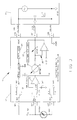
- the package of an integrated circuit 12 made in accordance with the invention includes eight pins comprising a reference capacitor drive pin 1 (REF), an input signal detect pin 2 (DET), a guard or shield connection pin 3 (SHLD), a sensor (variable) capacitor drive pin 4 (VAR), a power supply or V dd connection 8 (VDD), an output voltage pin 7 (OUT), a low pass filter capacitor pin 6 (FLT) and a ground or Vss pin 5 (VSS).
- a sensor 10 made in accordance with the invention includes a variable capacitor C VAR and reference capacitor C REF connected to pins 4 and 1 respectively and to a common connection at pin 2.
- circuit 12 is connected at pin 7, through various filter capacitors to be discussed infra, to electronic control unit (ECU) 14 with a +5 volt supply 14a and a ground 14b connected between unit 14 and pins 8 and 5, respectively.
- ECU electronice control unit
- Parasitic capacitors C Rpar and C Vpar , C Par and EMC capacitors C EMC are shown for a typical application along with a shield capacitor C SHLD , load capacitor C LOAD . supply voltage capacitor C VDD and filter capacitor C FLT and R SERIES resistors.
- the Fig. 1 system includes an offset stage 18 and gain stage 20 to level shift and amplify the buffer stage output voltage V F so that the output voltage of circuit 12 swings from V SS to V DD when the pressure on the sensor goes from 0 to maximum.
- the system provides for adjustment of bias and the amplification factor gain over a wide range as indicated in the transducer output voltage versus stimulus graph shown in Fig. 2 with the bias adjusted between V Hclp and V Lclp clamped voltages and the gain slope adjusted providing a low calibration point at C ref /C varL and a high calibration point at C ref /C varH .
- Another optional feature provided in the system is an inverted output as indicated in dashed lines in the graph.
- integrated circuit 12 comprises first and second single pole, double throw (SPDT) phase switches, ⁇ A and a SPDT phase switch ⁇ B.
- the phase ⁇ B switch is coupled to an input buffer 16 having a negative input connected to the normally closed position of ⁇ B switch, ⁇ B nc and a positive input connected to the normally open position of ⁇ B switch ⁇ B no .
- An integrating resistor R int although not necessary, is shown connected between the normally open position ⁇ B no and the positive input of input buffer 16 and an integrating capacitor C int is connected between the positive input and analog ground.
- the output V F of input buffer 16 is connected to its negative input and to the normally closed position ⁇ A nc of a phase switch ⁇ A at the variable node 4.
- the normally open position ⁇ A no of the phase switch ⁇ A is connected to V VAR .
- the other phase switch ⁇ A is connected to the reference node 1 with its normally closed position ⁇ A nc connected to analog ground and its normally open position ⁇ A no connected to V REF .
- the output V F is connected to a bias section 18 and in turn to a gain section 20.
- a phase logic section 22 having an oscillator 24 provides pulses to control the positions of the phase switches ⁇ A, ⁇ B. Calibration of the circuit is provided by section 26.
- the output voltage of the sensor circuit is fed to the electronic control unit 14 of an automobile or the like.
- Unit 14 contains the +5V volt supply and an analog-to-digital converter which converts the output voltage into a digital word for further processing by the microprocessor " ⁇ P" of the unit 14, thereby maintaining accuracy regardless of the supply voltage.
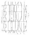
- phase switches ⁇ A and ⁇ B are cycled through three distinct phases during one sample cycle, viz., the charge reference phase, the charge redistribution phase and the error voltage integrating phase, shown in Fig. 4 along with the voltages at the reference (REF), detect (DET) and variable (VAR) pins.
- the SPDT switches ⁇ A and ⁇ B are in the normally closed (nc) position, as shown in Fig. 3.
- the reference capacitor C REF is connected to analog ground VSS and sensor capacitor C VAR is shorted to V F .
- the charge reference phase is selected to be sufficiently long for the C REF and C VAR voltages to settle before entering the charge distribution phase.
- the switches ⁇ A nc and ⁇ B nc open at the end of the charge reference phase and the two ⁇ A no switches close.
- the ⁇ A switches are break-before-make switches in order to prevent loss of reference charge on capacitors C REF and C VAR .
- all the switches are selected to be of low leakage and are switching charge compensated in order to prevent errors at the detect node (DET).
- the switch ⁇ B no stays open for the duration of the charge redistribution phase. At the end of this phase the switch ⁇ B no closes so that the integrating capacitor C int is then charged depending on the voltage difference between voltage V F and the voltage at the detect (DET) node.
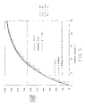
- V F V VAR + V REF * C REF /C VAR 0 * (1 - d/D)
- Each sample cycle reduces the error from a previous cycle by the ratio of the capacitors C VAR to (C REF + C VAR + C int ).
- the frequency response can be modified by changing the value of the integrating capacitor C int , that is, in a finished integrated circuit the frequency response can be reduced by adding an external capacitor between the detect pin (DET) and the analog ground pin (VSS). Further, the transient response or band width of the input stage is affected by resistor R int
- the input stage providing voltage V F functions as described above with reference to Fig. 3.
- the signal V F from the input stage needs bias and gain adjustments.
- the adjustment ranges are so large that these functions are distributed over two stages, namely, a coarse adjust bias and gain stage and a fine bias and gain stage.
- the invert/non-invert stage allows the selection of the output voltage polarity.
- Its output voltage V CLP covers the V SS to V DD range.
- the output amplifier has a gain of 1 or less in order to select the output voltage range. Fault detection circuits report faults by forcing the output voltage outside its normal range of operation.
- Integrated circuit 12 functions as a sampled system, as noted above.
- the timing signals ⁇ A and ⁇ B are generated internally and are derived from on-chip oscillator 24. In their high and low states, these signals will close and open their respective switches.
- the oscillator frequency, from which the timing signals are derived, is selected to be as low as possible to reduce EMC susceptibility.
- EMC suppression filters, as seen in Fig. 1, may be employed in the supply line to the oscillator section.
- the SPDT switches ⁇ A and ⁇ B must be break-before-make switches in order to prevent reference charge loss and to prevent excessive cross-over current spikes.
- the timing diagram of Fig. 4 shows that for the duration t BBM both switches ⁇ A nc and A no and B nc and B no are off.
- the switches ⁇ B nc and ⁇ A nc must also break-before-make in order to prevent unwanted charge injection on capacitor C int .
- the input stage comprises phase switches ⁇ A and ⁇ B, the integrating network resistor R int and capacitor C int and the unity-gain buffer 16.
- An important function of input stage buffer 16 is to supply a source current spike to charge the sensor capacitor C VAR and the parasitic capacitor C VPAR at the VAR node 4. These currents are turned on by the nc switches of ⁇ A and ⁇ B at the beginning of the reference phase.
- All amplifiers in integrated circuit 12 are referenced to an internal common mode voltage.
- this voltage is set to V DD /2 by means of the voltage divider with resistors R CM .
- This voltage is buffered by means of a unity gain amplifier 28a.
- coarse bias and gain stage 30 includes an exponential potentiometric 4 bit gain DAC including resists R in , R g and R f adjustably connected to the negative input of amplifier 30a and an 8 bit potentiometric bias DAC1 including resistors 256 Rb and 110 Rb adjustably connected to the positive input of amplifier 30a.
- the output V B of amplifier 30a is connected to resistor R f , to sensor fault detection section 40, to be discussed, and to a temperature compensating network 42a, to be discussed, whose output is connected through resistor Rgm to the negative input of fine bias and gain stage amplifier 32a.
- output V B is connected to gain DAC2 whose output R dac is connected to the negative input of amplifier 32a along with the output of bias DAC2 and temperature compensating network 42b, to be discussed.
- Output V B is also connected to the negative input of amplifier 32a through 0.333 R dac and the output V G of amplifier 32a is fed back to the negative input through resistor 0.8333 R dac .
- the output V G of amplifier 32a is connected to the negative input of non-invert/invert stage amplifier 34 through a resistor Ri and with the output of the amplifier fed back to its negative input through another resistor Ri.
- Switch S INV is used to switch the output V CLP from amplifier 32a, shown in a default position, which provides output voltage which increases with increasing transducer capacitance C VAR , i.e., with increasing sensed pressure to an alternate position which causes the output voltage to decrease with increasing value of the transducer capacitance C VAR .
- the voltage V CLP is the input voltage for the output amplifier 36.
- the gain of the output stage is progammable in order to provide programmable output voltage clamping levels. Limiting the output voltage span results in the formation of forbidden output voltage bands just above V SS and just below V DD which can be used to report failures to the electronic control unit.
- a two bit DAC 36a is provided for controlling four spans with a default position of 100% for no clamping.
- An external filter capacitor can be added between the output and filter nodes 7 (OUT) and 6 (FLT) in order to limit bandwidth. Capacitor C noise limits the bandwidth to approximately 25k Hz which attenuates sample frequency noise at the output.
- the calibrated variable-capacitance sensor, as well as the circuit 12, may be temperature dependent.
- Fig. 9 shows a temperature compensation circuit which may be used to correct for thermal error.
- the bias and gain calibration of the assembled sensor is conducted at room temperature T1. Temperature compensation calibration is performed at a different temperature T2.
- the network 42 shown in the figure, permits this without affecting the T1 calibration.
- the network includes a gain amplifier 42c whose negative input is connected to adjustable resistor R t1 which is connected between resistors R lin and V dd and R lin and temperature dependent resistors R tc and V ss . The output is fed back to the negative input through resistor R gain and to the negative input of amplifier 42d through resistor R.
- the output of amplifier 42d is fed back to its negative input through a resistor R and through an adjustable resistor R tc connected to the output of amplifier 42c to provide an output l out which can be adjusted at temperature T2.
- the temperature compensation trim at temperature T2 requires writing to temporary TC compensation registers 46 while the transducer is operating from the permanent memory written at T1 in permanent memory 48.
- the memory registers include a set of temporary/permanent TI registers and a set of temporary/permanent T2 registers with the calibration procedure writing to either set.
- the pressure or acceleration transducer must be calibrated in order to meet different end use requirements as well as to correct for manufacturing variations in the capacitor values of the calibrated capacitor sensor. Calibration is typically conducted with a 5.0V supply voltage at 25° and at an elevated temperature for the TC cancellation trim.
- the programming sequence includes setting on-chip operating mode switches and entering coarse bias and gain DAC codes, fine bias and gain codes and temperature compensation DAC codes and after testing and iterating until the specification is met, storing the final switch settings in a reliable, non-volatile memory.
- the circuit includes fault detectors. If the fault reporting feature has been enabled during calibration and a fault is detected during normal operation of the sensor, then the output of the sensor will be pulled low to the V ss or GND rail which will be interpreted by the ECU 14 as a fault condition.
- the default for the fault reporting switch S FLT in Fig. 6 is open, i.e., no fault reporting.
- a sensor pass/fail detector is included in the circuit. If the sensor capacitor C VAR or the reference capacitor C REF should become an open or a short then the voltage at the output of the coarse gain stage V B will be outside the normal operating range which is 50% +/- 20% of V DD .
- the sensor fault detection 40 indicated in the block diagram of Fig. 6 comprises two threshold detectors (not shown).
- the circuit includes a self test 40a which is a parity check of the content of the permanent memory. If, during normal operation of the sensor, a parity failure is detected than this failure will activate the fault reporting feature, if the feature has been enabled during calibration, and will force the output of the circuit to the V ss rail.
- FIG. 10 A typical application is shown in Fig 10.
- the only external components needed tor proper operation of the circuit are the calibrated capacitance sensing element C VAR and the reference capacitor C REF .
- additional external components may be added in order to customize the performance of the transducer.
- such components can include external resistors R SERIES , R PULL UP , R PULL DOWN which make it possible to scale the output voltage range and to create clamping levels different from those provided by the circuits to accommodate certain failure detection schemes.
- the shielding pin SHLD provides a voltage source equal to the voltage at the DET pin and is used to guard the conductor runs connected to the DET input pin. This reduces leakage current into the sensitive DET pin.
- the external filter capacitor C FLT reduces the frequency response of the transducer.
- the EMC capacitors improve resistance to electro-magnetic noise coupled into the transducer case and cables to the transducer.
- the sensor connector 50 interconnects the circuit to the ECU 14 shown in Figs. 1, 3.
Landscapes
- Engineering & Computer Science (AREA)
- Power Engineering (AREA)
- Physics & Mathematics (AREA)
- General Physics & Mathematics (AREA)
- Measuring Fluid Pressure (AREA)
- Transmission And Conversion Of Sensor Element Output (AREA)
- Electronic Switches (AREA)
Abstract
Description
- ∈O =
- permitivity of free space (8.854 pF/m)
- Aeff =
- the effective sensor capacitance plate area (m2)
- D =
- the distance between the sensor capacitor plates when no pressure or force is applied (m)
- D-d =
- = the effective distance between the capacitor plates when pressure or force is applied (m)
- CVAR0 =
- CVAR at d = 0
Claims (15)
- A variable capacitive transducer comprising:a variable capacitor for providing an electrical signal responsive to the application of a mechanical stimulus being monitored and a reference capacitor connected to the variable capacitor to form a detect node;an electric circuit comprising an input buffer having a positive input, a negative input and an output, the detect node being connected to a phase B switch, which is switchable between a first configuration, in which the detect node is connected to the negative input and a second configuration, in which the detect node is connected to the positive input, and an integrating capacitor connected to the positive input;the reference capacitor being connected to a first phase A switch, which is switchable between a first configuration in which the reference capacitor is connected to a first reference voltage and a second configuration, in which the reference capacitor is connected to a second reference voltage;the variable capacitor being connected to a second phase A switch, which is switchable between a first position, in which the variable capacitor is connected to the output of the input buffer and a second position, in which the variable capacitor is connected to a third reference voltage; anda logic circuit for providing instructional cycles and connected to the respective phase switches to control the configuration of the phase switches so that for a first charge reference portion of each instructional cycle, phase A and phase B switches are in their respective first configurations, for a second charge redistribution portion of each instructional cycle the phase A switches are in their respective second configurations and for a third charge integration portion of each cycle the phase B switch is in its second configuration.
- A variable capacitive transducer according to claim 1, in which the first reference voltage is analog ground.
- A variable capacitive transducer according to claim 1 or claim 2, in which the third reference voltage is analog ground.
- A variable capacitive transducer according to any preceding claim, in which the phase B switch is a single-pole, double-throw switch, which has a normally closed contact connected to the negative input and a normally open contact connected to the positive input.
- A variable capacitive transducer according to any preceding claim, in which the first phase A switch is a single-pole, double-throw switch, which has a normally closed contact connected to the first reference voltage and a normally open contact connected to the second reference voltage.
- A variable capacitive transducer according to any preceding claim, in which the second phase A switch is a single-pole, double-throw switch, which has a normally closed contact connected to the output of the input buffer and a normally open contact connected to the third reference voltage.
- A variable capacitive transducer according to any preceding claim, further comprising an integrating resistor connected to the positive input of the input buffer.
- A variable capacitive transducer according to any preceding claim, further comprising a bias and gain stage having an amplifier having a positive and a negative input and an output, means for providing controllable gain coupled between the output of the input buffer and the negative input and means for providing controllable bias coupled between a power supply voltage and the positive input of the bias and gain stage amplifier.
- A variable capacitive transducer according to claim 8, in which the gain increases exponentially with a linear increase in a control signal.
- A variable capacitive transducer according to claim 8 or claim 9, in which the bias increases linearly with a linear increase in a control signal.
- A variable capacitive transducer according to any of claims 8 to 10, in which the means for providing controllable gain and/or the means for providing controllable bias comprises a digital-to-analog converter.
- A variable capacitive transducer according to any of claims 8 to 11, in which the gain of the gain stage is from 1.0 to 9.3 with a resolution at the output voltage of the gain stage from 0.6% to 2.8% of the supply voltage.
- A variable capacitive transducer according to any of claims 8 to 12, further comprising a fine bias and gain stage having an amplifier having a positive and a negative input and an output, means for providing controllable fine gain coupled between the output of the coarse bias and gain stage amplifier and the negative input of the fine bias and gain stage amplifier and means for providing controllable fine bias coupled between the power supply voltage and the negative input of the fine bias and gain stage amplifier and a reference voltage coupled to the positive input of the fine bias and gain amplifier.
- A variable capacitive transducer according to claim 13, in which the means for providing controllable fine gain and/or the means for providing controllable fine bias comprises a digital-to-analog converter.
- A variable capacitive transducer according to claim 13 or claim 14, in which the resolution of the fine bias stage reduces an output voltage of the bias stage of 2.8% of the supply voltage to approximately 0.1%.
Applications Claiming Priority (2)
| Application Number | Priority Date | Filing Date | Title |
|---|---|---|---|
| US45784099A | 1999-12-09 | 1999-12-09 | |
| US457840 | 1999-12-09 |
Publications (2)
| Publication Number | Publication Date |
|---|---|
| EP1106981A2 true EP1106981A2 (en) | 2001-06-13 |
| EP1106981A3 EP1106981A3 (en) | 2002-07-24 |
Family
ID=23818263
Family Applications (1)
| Application Number | Title | Priority Date | Filing Date |
|---|---|---|---|
| EP00310888A Withdrawn EP1106981A3 (en) | 1999-12-09 | 2000-12-07 | Capacitive transducer |
Country Status (2)
| Country | Link |
|---|---|
| EP (1) | EP1106981A3 (en) |
| JP (1) | JP2001221654A (en) |
Cited By (7)
| Publication number | Priority date | Publication date | Assignee | Title |
|---|---|---|---|---|
| DE102005063023A1 (en) * | 2005-12-14 | 2007-06-21 | Gerd Reime | Arrangement for monitoring an object |
| WO2007132422A1 (en) | 2006-05-17 | 2007-11-22 | Nxp B.V. | Capacitive mems sensor device |
| CN103026194A (en) * | 2010-05-27 | 2013-04-03 | 丹佛斯多能公司 | A resonance circuit having a variable resonance frequency |
| CN101448187B (en) * | 2007-11-14 | 2013-04-10 | 英飞凌科技股份有限公司 | Electronic circuits and electronic devices |
| DE102013201704A1 (en) * | 2013-02-01 | 2014-08-07 | Di-Soric Gmbh & Co. Kg | Capacitive sensor arrangement and capacitive measuring method with compensation of parasitic capacitances |
| CN104736972B (en) * | 2012-08-15 | 2017-03-08 | 罗伯特·博世有限公司 | capacitive sensor |
| DE102023112470B4 (en) * | 2022-05-11 | 2025-06-05 | Infineon Technologies Ag | Diagnosis of electrical faults in capacitive sensors |
Families Citing this family (12)
| Publication number | Priority date | Publication date | Assignee | Title |
|---|---|---|---|---|
| DE10357870B4 (en) * | 2003-12-11 | 2013-02-07 | Robert Bosch Gmbh | Sensor with symmetrical limitation of a signal |
| US20070196160A1 (en) * | 2004-03-18 | 2007-08-23 | Sakura Color Products Corporation | Tips for ball-point pens, roller ball pens or gel ink roller ball pens |
| JP2006064470A (en) * | 2004-08-25 | 2006-03-09 | Denso Corp | Electrical equipment control device |
| JP2006145367A (en) * | 2004-11-19 | 2006-06-08 | Mitsubishi Electric Corp | Acceleration sensor |
| DE102004056416A1 (en) * | 2004-11-23 | 2006-05-24 | Robert Bosch Gmbh | Accelerometer in a controller |
| JP5352905B2 (en) * | 2009-05-28 | 2013-11-27 | ルネサスエレクトロニクス株式会社 | Semiconductor device and touch sensor using the same |
| TWI463295B (en) * | 2011-10-28 | 2014-12-01 | Quanta Comp Inc | Reset and reboot circuit |
| KR101511695B1 (en) | 2014-06-17 | 2015-04-13 | 한국기술교육대학교 산학협력단 | sigma-delta circuit to compensate the capacitance mismatch for capacitive micro-accelerometers |
| KR101691714B1 (en) * | 2015-01-05 | 2017-01-09 | 한국기술교육대학교 산학협력단 | Filter Comprising Active Resistor and Sigma Delta Ripple Smoothing Circuit for Capacitive Micro Acceleration Sensor |
| WO2016111479A1 (en) * | 2015-01-05 | 2016-07-14 | 한국기술교육대학교 산학협력단 | Filter comprising active resistor, and sigma-delta modulator ripple smoothing circuit of capacitive micro-acceleration sensor using same |
| JP6804284B2 (en) * | 2016-12-14 | 2020-12-23 | 株式会社堀場エステック | Capacitive sensor |
| CN109029749B (en) * | 2018-08-17 | 2020-01-31 | 黑龙江天有为电子有限责任公司 | type water temperature circuit with collection ground offset and method thereof |
Family Cites Families (1)
| Publication number | Priority date | Publication date | Assignee | Title |
|---|---|---|---|---|
| US5770802A (en) * | 1997-04-16 | 1998-06-23 | Texas Instruments Incorporated | Sensor with improved capacitive to voltage converter integrated circuit |
-
2000
- 2000-12-07 EP EP00310888A patent/EP1106981A3/en not_active Withdrawn
- 2000-12-08 JP JP2000374497A patent/JP2001221654A/en active Pending
Cited By (13)
| Publication number | Priority date | Publication date | Assignee | Title |
|---|---|---|---|---|
| US7902841B2 (en) | 2005-12-14 | 2011-03-08 | Gerd Reime | Capacitive proximity sensor |
| WO2007068457A1 (en) * | 2005-12-14 | 2007-06-21 | Gerd Reime | Capacitive proximity sensor |
| DE102005063023A1 (en) * | 2005-12-14 | 2007-06-21 | Gerd Reime | Arrangement for monitoring an object |
| US8134375B2 (en) | 2006-05-17 | 2012-03-13 | Nxp B.V. | Capacitive MEMS sensor device |
| CN101443633A (en) * | 2006-05-17 | 2009-05-27 | Nxp股份有限公司 | Capacitive mems sensor device |
| CN101443633B (en) * | 2006-05-17 | 2011-03-16 | Nxp股份有限公司 | Capacitive MEMS sensor device |
| WO2007132422A1 (en) | 2006-05-17 | 2007-11-22 | Nxp B.V. | Capacitive mems sensor device |
| CN101448187B (en) * | 2007-11-14 | 2013-04-10 | 英飞凌科技股份有限公司 | Electronic circuits and electronic devices |
| CN103026194A (en) * | 2010-05-27 | 2013-04-03 | 丹佛斯多能公司 | A resonance circuit having a variable resonance frequency |
| CN104736972B (en) * | 2012-08-15 | 2017-03-08 | 罗伯特·博世有限公司 | capacitive sensor |
| DE102013201704A1 (en) * | 2013-02-01 | 2014-08-07 | Di-Soric Gmbh & Co. Kg | Capacitive sensor arrangement and capacitive measuring method with compensation of parasitic capacitances |
| DE102023112470B4 (en) * | 2022-05-11 | 2025-06-05 | Infineon Technologies Ag | Diagnosis of electrical faults in capacitive sensors |
| US12467816B2 (en) | 2022-05-11 | 2025-11-11 | Infineon Technologies Ag | Diagnosis of electrical failures in capacitive sensors |
Also Published As
| Publication number | Publication date |
|---|---|
| JP2001221654A (en) | 2001-08-17 |
| EP1106981A3 (en) | 2002-07-24 |
Similar Documents
| Publication | Publication Date | Title |
|---|---|---|
| US6058783A (en) | Sensor with improved capacitive to voltage converter integrated circuit | |
| JP2001221654A (en) | Variable capacitive transducer | |
| US6433554B1 (en) | Method and apparatus for in-range fault detection of condition responsive sensor | |
| US10983187B2 (en) | Measuring bridge arrangement with improved error detection | |
| US5024101A (en) | Power source circuit and bridge type measuring device with output compensating circuit utilizing the same | |
| US5231351A (en) | Magnetoresistive speed sensor processing circuit utilizing a symmetrical hysteresis signal | |
| US10268226B1 (en) | Voltage generating device and calibrating method thereof | |
| EP0975983A2 (en) | Capacitance detection system and method | |
| CN102472774A (en) | Wide dynamic range electrometer with a fast response | |
| KR102125891B1 (en) | Rf sensor in stacked transistors | |
| US5466976A (en) | Time constant detecting circuit and time constant adjusting circuit | |
| JP5071086B2 (en) | Passive probe device | |
| US6066976A (en) | Apparatus and method for improved dynamic range | |
| EP0088561B1 (en) | Capacitor monitoring circuit | |
| US6628147B2 (en) | Comparator having reduced sensitivity to offset voltage and timing errors | |
| US20200127624A1 (en) | Amplifier systems for measuring a wide range of current | |
| CN113691236B (en) | Temperature compensation broadband signal attenuation circuit and control method thereof | |
| US6053050A (en) | Signal conditioning system | |
| US10224909B1 (en) | Error elimination amplifier and motor control circuit using the same | |
| US6549138B2 (en) | Method and apparatus for providing detection of excessive negative offset of a sensor | |
| JP2618822B2 (en) | Capacitance sensor | |
| US8461913B2 (en) | Integrated circuit and a method for selecting a voltage in an integrated circuit | |
| DE10133525A1 (en) | Pressure measurement sensor for motor vehicle control can be switched between measurement and test modes with aging and temperature effects same in two modes | |
| CN120540473B (en) | A precision micro current source | |
| EP0846955A1 (en) | Sensor test arrangement and method |
Legal Events
| Date | Code | Title | Description |
|---|---|---|---|
| PUAI | Public reference made under article 153(3) epc to a published international application that has entered the european phase |
Free format text: ORIGINAL CODE: 0009012 |
|
| AK | Designated contracting states |
Kind code of ref document: A2 Designated state(s): AT BE CH CY DE DK ES FI FR GB GR IE IT LI LU MC NL PT SE TR |
|
| AX | Request for extension of the european patent |
Free format text: AL;LT;LV;MK;RO;SI |
|
| PUAL | Search report despatched |
Free format text: ORIGINAL CODE: 0009013 |
|
| AK | Designated contracting states |
Kind code of ref document: A3 Designated state(s): AT BE CH CY DE DK ES FI FR GB GR IE IT LI LU MC NL PT SE TR |
|
| AX | Request for extension of the european patent |
Free format text: AL;LT;LV;MK;RO;SI |
|
| RIC1 | Information provided on ipc code assigned before grant |
Free format text: 7G 01L 1/00 A, 7G 01D 5/24 B, 7G 01L 27/00 B |
|
| AKX | Designation fees paid | ||
| REG | Reference to a national code |
Ref country code: DE Ref legal event code: 8566 |
|
| STAA | Information on the status of an ep patent application or granted ep patent |
Free format text: STATUS: THE APPLICATION IS DEEMED TO BE WITHDRAWN |
|
| 18D | Application deemed to be withdrawn |
Effective date: 20030125 |