EP1104046A2 - Circuit forming method and circuit connection structure in electrical connection box - Google Patents
Circuit forming method and circuit connection structure in electrical connection box Download PDFInfo
- Publication number
- EP1104046A2 EP1104046A2 EP00125592A EP00125592A EP1104046A2 EP 1104046 A2 EP1104046 A2 EP 1104046A2 EP 00125592 A EP00125592 A EP 00125592A EP 00125592 A EP00125592 A EP 00125592A EP 1104046 A2 EP1104046 A2 EP 1104046A2
- Authority
- EP
- European Patent Office
- Prior art keywords
- pressure
- circuit board
- bus
- contact knife
- hole
- Prior art date
- Legal status (The legal status is an assumption and is not a legal conclusion. Google has not performed a legal analysis and makes no representation as to the accuracy of the status listed.)
- Granted
Links
Images
Classifications
-
- H—ELECTRICITY
- H05—ELECTRIC TECHNIQUES NOT OTHERWISE PROVIDED FOR
- H05K—PRINTED CIRCUITS; CASINGS OR CONSTRUCTIONAL DETAILS OF ELECTRIC APPARATUS; MANUFACTURE OF ASSEMBLAGES OF ELECTRICAL COMPONENTS
- H05K1/00—Printed circuits
- H05K1/02—Details
- H05K1/14—Structural association of two or more printed circuits
- H05K1/144—Stacked arrangements of planar printed circuit boards
-
- H—ELECTRICITY
- H01—ELECTRIC ELEMENTS
- H01R—ELECTRICALLY-CONDUCTIVE CONNECTIONS; STRUCTURAL ASSOCIATIONS OF A PLURALITY OF MUTUALLY-INSULATED ELECTRICAL CONNECTING ELEMENTS; COUPLING DEVICES; CURRENT COLLECTORS
- H01R13/00—Details of coupling devices of the kinds covered by groups H01R12/70 or H01R24/00 - H01R33/00
- H01R13/46—Bases; Cases
- H01R13/502—Bases; Cases composed of different pieces
- H01R13/504—Bases; Cases composed of different pieces different pieces being moulded, cemented, welded, e.g. ultrasonic, or swaged together
-
- H—ELECTRICITY
- H01—ELECTRIC ELEMENTS
- H01R—ELECTRICALLY-CONDUCTIVE CONNECTIONS; STRUCTURAL ASSOCIATIONS OF A PLURALITY OF MUTUALLY-INSULATED ELECTRICAL CONNECTING ELEMENTS; COUPLING DEVICES; CURRENT COLLECTORS
- H01R4/00—Electrically-conductive connections between two or more conductive members in direct contact, i.e. touching one another; Means for effecting or maintaining such contact; Electrically-conductive connections having two or more spaced connecting locations for conductors and using contact members penetrating insulation
- H01R4/02—Soldered or welded connections
- H01R4/021—Soldered or welded connections between two or more cables or wires
-
- H—ELECTRICITY
- H01—ELECTRIC ELEMENTS
- H01R—ELECTRICALLY-CONDUCTIVE CONNECTIONS; STRUCTURAL ASSOCIATIONS OF A PLURALITY OF MUTUALLY-INSULATED ELECTRICAL CONNECTING ELEMENTS; COUPLING DEVICES; CURRENT COLLECTORS
- H01R4/00—Electrically-conductive connections between two or more conductive members in direct contact, i.e. touching one another; Means for effecting or maintaining such contact; Electrically-conductive connections having two or more spaced connecting locations for conductors and using contact members penetrating insulation
- H01R4/24—Connections using contact members penetrating or cutting insulation or cable strands
- H01R4/2416—Connections using contact members penetrating or cutting insulation or cable strands the contact members having insulation-cutting edges, e.g. of tuning fork type
- H01R4/242—Connections using contact members penetrating or cutting insulation or cable strands the contact members having insulation-cutting edges, e.g. of tuning fork type the contact members being plates having a single slot
-
- H—ELECTRICITY
- H05—ELECTRIC TECHNIQUES NOT OTHERWISE PROVIDED FOR
- H05K—PRINTED CIRCUITS; CASINGS OR CONSTRUCTIONAL DETAILS OF ELECTRIC APPARATUS; MANUFACTURE OF ASSEMBLAGES OF ELECTRICAL COMPONENTS
- H05K1/00—Printed circuits
- H05K1/02—Details
- H05K1/0213—Electrical arrangements not otherwise provided for
- H05K1/0263—High current adaptations, e.g. printed high current conductors or using auxiliary non-printed means; Fine and coarse circuit patterns on one circuit board
-
- H—ELECTRICITY
- H05—ELECTRIC TECHNIQUES NOT OTHERWISE PROVIDED FOR
- H05K—PRINTED CIRCUITS; CASINGS OR CONSTRUCTIONAL DETAILS OF ELECTRIC APPARATUS; MANUFACTURE OF ASSEMBLAGES OF ELECTRICAL COMPONENTS
- H05K2201/00—Indexing scheme relating to printed circuits covered by H05K1/00
- H05K2201/09—Shape and layout
- H05K2201/09009—Substrate related
- H05K2201/09063—Holes or slots in insulating substrate not used for electrical connections
-
- H—ELECTRICITY
- H05—ELECTRIC TECHNIQUES NOT OTHERWISE PROVIDED FOR
- H05K—PRINTED CIRCUITS; CASINGS OR CONSTRUCTIONAL DETAILS OF ELECTRIC APPARATUS; MANUFACTURE OF ASSEMBLAGES OF ELECTRICAL COMPONENTS
- H05K2201/00—Indexing scheme relating to printed circuits covered by H05K1/00
- H05K2201/10—Details of components or other objects attached to or integrated in a printed circuit board
- H05K2201/10227—Other objects, e.g. metallic pieces
- H05K2201/10272—Busbars, i.e. thick metal bars mounted on the PCB as high-current conductors
-
- H—ELECTRICITY
- H05—ELECTRIC TECHNIQUES NOT OTHERWISE PROVIDED FOR
- H05K—PRINTED CIRCUITS; CASINGS OR CONSTRUCTIONAL DETAILS OF ELECTRIC APPARATUS; MANUFACTURE OF ASSEMBLAGES OF ELECTRICAL COMPONENTS
- H05K2201/00—Indexing scheme relating to printed circuits covered by H05K1/00
- H05K2201/10—Details of components or other objects attached to or integrated in a printed circuit board
- H05K2201/10431—Details of mounted components
- H05K2201/10507—Involving several components
- H05K2201/1053—Mounted components directly electrically connected to each other, i.e. not via the PCB
-
- H—ELECTRICITY
- H05—ELECTRIC TECHNIQUES NOT OTHERWISE PROVIDED FOR
- H05K—PRINTED CIRCUITS; CASINGS OR CONSTRUCTIONAL DETAILS OF ELECTRIC APPARATUS; MANUFACTURE OF ASSEMBLAGES OF ELECTRICAL COMPONENTS
- H05K2201/00—Indexing scheme relating to printed circuits covered by H05K1/00
- H05K2201/10—Details of components or other objects attached to or integrated in a printed circuit board
- H05K2201/10613—Details of electrical connections of non-printed components, e.g. special leads
- H05K2201/10621—Components characterised by their electrical contacts
- H05K2201/10651—Component having two leads, e.g. resistor, capacitor
-
- H—ELECTRICITY
- H05—ELECTRIC TECHNIQUES NOT OTHERWISE PROVIDED FOR
- H05K—PRINTED CIRCUITS; CASINGS OR CONSTRUCTIONAL DETAILS OF ELECTRIC APPARATUS; MANUFACTURE OF ASSEMBLAGES OF ELECTRICAL COMPONENTS
- H05K3/00—Apparatus or processes for manufacturing printed circuits
- H05K3/10—Apparatus or processes for manufacturing printed circuits in which conductive material is applied to the insulating support in such a manner as to form the desired conductive pattern
- H05K3/20—Apparatus or processes for manufacturing printed circuits in which conductive material is applied to the insulating support in such a manner as to form the desired conductive pattern by affixing prefabricated conductor pattern
- H05K3/202—Apparatus or processes for manufacturing printed circuits in which conductive material is applied to the insulating support in such a manner as to form the desired conductive pattern by affixing prefabricated conductor pattern using self-supporting metal foil pattern
-
- Y—GENERAL TAGGING OF NEW TECHNOLOGICAL DEVELOPMENTS; GENERAL TAGGING OF CROSS-SECTIONAL TECHNOLOGIES SPANNING OVER SEVERAL SECTIONS OF THE IPC; TECHNICAL SUBJECTS COVERED BY FORMER USPC CROSS-REFERENCE ART COLLECTIONS [XRACs] AND DIGESTS
- Y10—TECHNICAL SUBJECTS COVERED BY FORMER USPC
- Y10S—TECHNICAL SUBJECTS COVERED BY FORMER USPC CROSS-REFERENCE ART COLLECTIONS [XRACs] AND DIGESTS
- Y10S439/00—Electrical connectors
- Y10S439/949—Junction box with busbar for plug-socket type interconnection with receptacle
Definitions
- the present invention relates to a circuit forming method and a circuit connection structure in an electrical connection box for use in a vehicle, for example.
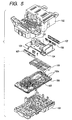
- an electronic circuit board 104 provided with electronic parts 103 between a lower case portion 101 and an upper case portion 102 constituting the electrical connection box, and an insulating board 106 provided with bus-bars 105 are generally housed in a laminated form as shown in Fig. 5.
- the electrical connection of the electronic parts 103 to the bus-bars 105 is accomplished by fitting a connector housing 107 retaining female terminals 108 to an edge portion of an electronic circuit board 104 and stacking the electronic circuit board 104 in this state on top of the insulating board 106 thereby to fit bus-bar tabs (male terminals) 105a with the bus-bars 105 in an upright condition into the respective female terminals of the connector housing 107.
- An insulating spacer 109 is provided between the electronic circuit board 104 and the insulating board 106 to avoid unnecessary electrical connection.
- the edge portion of the electronic circuit board 104 requires the female terminals 108 and the connector housing 107 so as to electrically connect the electronic parts 103 to the respective bus-bars 105, so that the number of parts tends to increase.
- bus-bar tab 105a connected to the female terminal 108 is formed by processing the edge portion of the bus-bar 105, any intermediate part of the bus-bar 105 cannot be connected to the female terminal 108 and when one bus-bar is connected to two or more connecting parts, for example, it is needed to use the same number of bus-bars as the number of connecting parts. Consequently, the utilization efficiency of the space for used in arranging the bus-bars has been poor.
- An object of the present invention is to solve the foregoing conventional technical problems and to provide a circuit forming method and a circuit connection structure that are capable of making smaller an electronic circuit board as well as reducing the number of parts.
- a circuit forming method in an electrical connection box according to the invention with an electronic circuit board and an insulating board being stacked up and housed therein comprising the steps of providing not only a through-hole in the electronic circuit board but also lead wires or electric wires of electronic parts in a manner straddling the through-hole, providing the bus-bars on the insulating board so that the upright pressure-contact knife-edges of the respective bus-bars may be arranged in a position corresponding to the through-hole of the insulating board, and stacking up the electronic circuit board and the insulating board by moving both the boards close to each other in such a condition that the pressure-contact knife-edges are passing through the through-hole, and pressure-welding the leadwires or electric wires to the respective pressure-contact knife-edges.
- a circuit connection structure comprising: an electronic circuit board having a through-hole, the electronic circuit board being provided with lead wires or electric wires of electronic parts in a manner straddling the through-hole, and an insulating board provided with bus-bars having upright pressure-contact knife-edges electrically connected to the lead wires or electric wires, wherein the electronic circuit board and the insulating board are stacked up by relatively moving both the boards close to each other in such a condition that the pressure-contact knife-edges are passing through the through-hole; and the lead wires or electric wires are pressure-welded to the respective pressure-contact knife-edges.
- the lead wires are pressure-welded to the respective pressure-contact knife-edges passed through the through-hole provided in the electronic circuit board in this circuit forming method and the circuit connection structure, the space for use in fitting the female terminals to the edge portion of the board in the prior art can be dispensed with, which results in making it possible to reduce the size of the electronic circuit board.
- the pressure-contact knife-edges are directly pressure-welded to the respective lead wires, so that female terminals and the connector housing necessitated in the prior art can be omitted, which results in reducing the number of parts.
- the pressure-contact knife-edges are formed separately from the respectivebus-bars, andthepressure-contact knife-edges may be fitted to the respective bus-bars in such a condition that the former has been electrically connected to the latter.
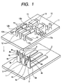
- Fig. 1 is an exploded perspective view of a bus-bar connection structure in an electrical connection box embodying the invention.
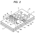
- Fig. 2 is a perspective view of the bus-bar connection structure in the electrical connection box according to the embodiment of the invention.
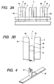
- Fig. 3A is an elevational view of the vicinity of the pressure-welded portion of the bus-bar connection structure in the electrical connection box according to the embodiment of the invention.
- Fig. 3B is a partial enlarged view of the portion above.
- Fig. 4 is a perspective view explanatory of another form of pressure-contact knife-edge usable according to the invention.
- Fig. 5 is a perspective view of a bus-bar connection structure in a conventional electrical connection box.
- Fig. 1 is an exploded perspective view of a circuit connection structure in an electrical connection box embodying the invention
- Fig. 2 is a perspective view of the circuit connection structure.
- the circuit connection structure is retained in a space formed between a lower case portion and an upper case portion (these being not shown) constituting the electrical connection box, an insulating board 1 being provided on the lower side and an electronic circuit board 10 being provided on the upper side.
- a plurality of bus-bars 2, three of them in the example of Fig. 1, are arranged side by side on the surface of and in the width direction of the insulating board 1, and the edge portion of each bus-bar 2 is made an upright pressure-contact knife-edge 3.
- the pressure-contact knife-edge 3 has a slot 4, and a knife edge is formed on both vertical edge faces 4a and 4b of the slot 4 and on an arcuate edge face 4c therebetween. Further, a chipped tilted guide portion 4e is formed in the upper edge portion of each of the edge faces 4a and 4b.
- a wiring pattern (not shown) is formed on the undersurface of the electronic circuit board 10, and a number of electronic parts 11 electrically connected to the predetermined wiring pattern are mounted thereon.
- Part of the electronic parts are electronic parts 14, each of which has lead wires 12 and 13 on its respective both sides as external terminals and there are provided three of the electronic parts 14 in the example of Fig. 1.
- the electronic parts 14 include, for example, resistors, capacitors or diodes.
- the lead wires 12 and 13 are made of electroconductive material such as copper and aluminum and as shown in Fig. 1 have vertical portions 12a and 13a and horizontal portions 12b and 13b, respectively.
- the horizontal portions 12b on one side are provided in a manner striding over a through-hole 15.
- the electronic parts 14 are fitted to the electronic circuit board 10 by inserting the vertical portions 12a and 13a into holes provided in the electronic circuit board 10 and also electrically connected thereto by soldering the vertical portions 12a and 13a to the wiring pattern (not shown) formed on the undersurface of the electronic circuit board 10.
- the through-hole 15 is used to insert the pressure-contact knife-edges 3 to the extent that they are passed therethrough.
- the width of the through-hole 15 is slightly greater than the thickness of each pressure-contact knife-edge 3 and the length thereof is slight greater than the distance between the outer sides 3a and 3a of both the outer pressure-contact knife-edges 3 out of three of them.
- Either insulating board 1 or electronic circuit board 10 may be made first.
- the insulating board 1 out of the insulating board 1 and the electronic circuit board 10 thus arranged is set inside the lower case portion (not shown) and then the spacer (not shown) is inserted. Subsequently, the electronic circuit board 10 is moved closer (lowered) to the insulating board 1 while the three pressure-contact knife-edges are passed through the through-hole 15. Even though the position of the lead wires 12 relative to that of the respective slots 4 at this time, each lead wire 12 is guided by the tilted guide portion 4e formed above the slot 4 to ensure that the lead wires 12 enter the slots 4. After this, the lead wires 12 of the electronic part 14 and the bus-bars 2 are pressure-welded.
- the pressure-welding is meant that as shown in Fig. 3A the horizontal portion 12b of each lead wire 12 enters the inner side of the slot 4 and that as shown in Fig. 3B the slot 4 is brought into contact with the horizontal portion 12b of the lead wire 12 whereby to make the lead wire 12 of the electronic part 14 electrically contact the bus-bar 2.
- the space (not shown) made of insulating material is held between the insulating board 1 and the electronic circuit board 10 so as to prevent the electrical connection between the wiring pattern formed on the undersurface of the electronic circuit board 10 and the bus-bars 2 provided on the surface of the insulating board 1.
- the circuit connection structure according to this embodiment of the invention is obtained by the circuit forming method thus implemented.
- the dimension of the estrangement between the edge faces of the slot 4 is set slight shorter than the diameter of the horizontal portion 12b of each lead wire 12, and the height of the horizontal portion 12b of the lead wire 12 from the electronic circuit board 10 is so arranged that what is lower than the tilted guide portions 4e of the respective edges faces 4a and 4b of the slot 4 is brought into contact with the horizontal portion 12b in such a state that the insulating board 1 has been placed on top of the electronic circuit board 10.
- the lead wires 12 are pressure-welded to the respective pressure-contact knife-edges passed through the through-hole 15 provided in the electronic circuit board 10 according to this embodiment of the invention, the space for use in fitting the female terminals 108 to the edge portion of the board in the prior art can be dispensed with, which results in making it possible to reduce the size of the electronic circuit board 10.
- the pressure-contact knife-edges 3 are directly pressure-welded to the respective lead wires 12, so that female terminals 108 and the connector housing 107 necessitated in the prior art can be omitted, which results in reducing the number of parts.
- the bus-bars 2 can be arranged for common use.
- the pressure-contact knife-edge 3 as the bus-bar tab is formed in the end portion of each bus-bar 2 itself as shown in Fig. 1 according to the above embodiment of the invention
- the invention is not limited to this arrangement but may be arranged as shown in Fig. 4 so as to form a bus-bar 20 and a pressure-contact knife-edge 21 separately and to have the pressure-contact knife-edge 21 fitted to the bus-bar 20 by pressure-welding.
- the pressure-contact knife-edge 21 may be fitted to the desired position of the bus-bar 20, for example, the mid position or end portion of the bus-bar 20 as shown in Fig. 4 and any number of pressure-contact knife-edges may be fitted thereto.
- the advantage in this case is that the utilization efficiency of the space for use in disposing the bus-bars becomes improvable thereby.
- the invention is not limited to this arrangement but may be equally applicable to a case where conductors of lead wires as electronic parts are externally covered wires, or bare or covered electric wires provided to electronic parts for external connection.
- the bare and the covered lead wires are intended for use in supporting the electronic parts in addition to the electrical connection.
- the bare and covered lead wires are such that they are not strong enough to support the electronic parts but comparatively soft and usable in place of the wiring pattern, for example.
- comparatively soft electric wires are applied to the pressure-contact technology according to the invention, they should preferably have desired hardness, whereby they are prevented from escaping when pressed down by the pressure-contact knife-edges.
- the insulating condition can be secured relative to any other wiring pattern or electronic part and this is advantageous in that a short circuit is preventable.
- the lead wires are pressure-welded to the respective pressure-contact knife-edges passed through the through-hole provided in the electronic circuit board in this circuit forming method and the circuit connection structure, the space for use in fitting the female terminals to the edge portion of the board in the prior art can be dispensed with, which results in making it possible to reduce the size of the electronic circuit board.
- the pressure-contact knife-edges are directly pressure-welded to the respective lead wires, so that female terminals and the connector housing necessitated in the prior art can be omitted, which results in reducing the number of parts.
- the pressure-contact knife-edges are formed separately from the respective bus-bars and when the pressure-contact knife-edges are be fitted to the respective bus-bars in such a condition that the former has been electrically connected to the latter, any number of pressure-contact knife-edges can freely be provided to the end portion or mid position of the bus-bar, whereby the utilization efficiency of the space for use in disposing the bus-bars becomes improvable.
Abstract
Description
Claims (5)
- A method of forming a circuit in an electrical connection box having an electronic circuit board and an insulating board being stacked up and housed in the connection box, the method comprising:providing a through-hole in the electronic circuit board;providing a lead wire or electric wire of an electronic component in a manner straddling the through-hole;providing the bus bar on the insulating board so that a upright pressure-contact knife-edge of the bus-bar is arranged in a position corresponding to the through-hole of the insulating board;moving the electronic circuit board and the insulating board close to each other in such a condition that the pressure-contact knife-edges are passing through the through-hole;stacking up the electronic circuit board and the insulating board; andpressure-welding the lead wire or electric wire to the pressure-contact knife-edges.
- A circuit connection structure comprising:an electronic circuit board having a through-hole, the electronic circuit board having a lead wire or electric wire of an electronic component in a manner straddling the through-hole, andan insulating board having a bus-bar having a upright pressure-contact knife-edge electrically connected to the lead wire or electric wire,wherein the electronic circuit board and the insulating board are stacked up by relatively moving both the boards close to each other in such a condition that the pressure-contact knife-edge are passing through the through-hole; and the lead wire or electric wire are pressure-welded to the pressure-contact knife-edge.
- The circuit connection structure as claimed in claim 2, wherein the pressure-contact knife-edge is formed separately from the bus-bar; and
the pressure-contact knife-edge is fitted to the bus-bar in such a condition that the pressre-contact knife-edge has been electrically connected to the bus-bar. - An electrical connection box comprising:a circuit board having an electrical component and a lead wire connected to the electrical component, the circuit board defining a hole above which the lead wire passes; andan insulating board stacked on the circuit board, the insulating board having a bus bar,wherein the bus bar passes through the hole and being engaged with the lead wire of the circuit board.
- The electric connection box as claimed in claim 4, wherein the bus bar comprises a branch portion connected to the bus bar, the branch portion is engaged with the lead wire of the circuit board.
Applications Claiming Priority (2)
| Application Number | Priority Date | Filing Date | Title |
|---|---|---|---|
| JP33261099A JP3457239B2 (en) | 1999-11-24 | 1999-11-24 | Circuit forming method and circuit connection structure in electrical junction box |
| JP33261099 | 1999-11-24 |
Publications (3)
| Publication Number | Publication Date |
|---|---|
| EP1104046A2 true EP1104046A2 (en) | 2001-05-30 |
| EP1104046A3 EP1104046A3 (en) | 2002-06-26 |
| EP1104046B1 EP1104046B1 (en) | 2004-04-14 |
Family
ID=18256880
Family Applications (1)
| Application Number | Title | Priority Date | Filing Date |
|---|---|---|---|
| EP00125592A Expired - Lifetime EP1104046B1 (en) | 1999-11-24 | 2000-11-22 | Circuit forming method and circuit connection structure in electrical connection box |
Country Status (4)
| Country | Link |
|---|---|
| US (1) | US6409522B1 (en) |
| EP (1) | EP1104046B1 (en) |
| JP (1) | JP3457239B2 (en) |
| DE (1) | DE60009834T2 (en) |
Cited By (2)
| Publication number | Priority date | Publication date | Assignee | Title |
|---|---|---|---|---|
| DE10338297B4 (en) * | 2002-09-11 | 2007-04-05 | Sumitomo Wiring Systems, Ltd., Yokkaichi | busbar |
| EP2330865A1 (en) * | 2009-12-03 | 2011-06-08 | Eberspächer catem GmbH & Co. KG | Electric heating device |
Families Citing this family (13)
| Publication number | Priority date | Publication date | Assignee | Title |
|---|---|---|---|---|
| JP3724372B2 (en) * | 2000-12-28 | 2005-12-07 | 住友電装株式会社 | Electrical junction box |
| DE10129840B4 (en) * | 2001-06-21 | 2020-10-08 | Robert Bosch Gmbh | Electric device |
| US7167377B2 (en) * | 2001-11-26 | 2007-01-23 | Sumitoo Wiring Systems, Ltd. | Circuit-constituting unit and method of producing the same |
| DE20311184U1 (en) * | 2003-07-21 | 2004-02-19 | Tyco Electronics Amp Gmbh | Junction box for connection to a solar panel |
| US7074051B2 (en) * | 2004-02-17 | 2006-07-11 | Hewlett-Packard Development Company, L.P. | System and method for electrically interconnecting boards |
| US20060048968A1 (en) * | 2004-09-03 | 2006-03-09 | Wei-Kuang Chen | Construction for DC to AC power inverter |
| US7548411B2 (en) * | 2004-10-29 | 2009-06-16 | Hitachi, Ltd. | Electronic circuit structure, power supply apparatus, power supply system, and electronic apparatus |
| US20060256533A1 (en) * | 2005-05-13 | 2006-11-16 | Lear Corporation | Thermally dissipating and power dispersing adhesively bonded metal-printed circuit board structure |
| JP4888359B2 (en) * | 2007-02-23 | 2012-02-29 | 株式会社アドヴィックス | Electronic control unit and manufacturing method thereof |
| US7716821B2 (en) * | 2007-12-12 | 2010-05-18 | Sauer-Danfoss Inc. | Method of manufacturing a circuit board assembly for a controller |
| JP5348495B2 (en) * | 2009-11-26 | 2013-11-20 | 株式会社オートネットワーク技術研究所 | Circuit structure and electrical junction box |
| DE102010029494A1 (en) * | 2010-05-31 | 2011-12-01 | Robert Bosch Gmbh | Connection system for connecting e.g. printed circuit board with electronic component e.g. resistor, to form electrical circuit, has contact structure with springs for pressing contact wire during insertion into wire-receiving sections |
| CN104603901A (en) * | 2012-08-21 | 2015-05-06 | 矢崎总业株式会社 | Electronic component assembly, connection structure of electronic component assembly and terminal fitting, and electrical connection box having electronic component assembly |
Citations (4)
| Publication number | Priority date | Publication date | Assignee | Title |
|---|---|---|---|---|
| US5509812A (en) * | 1994-06-20 | 1996-04-23 | Molex Incorporated | Cable tap assembly |
| US5709567A (en) * | 1996-07-25 | 1998-01-20 | General Motors Corporation | Press fit stamped buss |
| EP0887884A2 (en) * | 1997-05-28 | 1998-12-30 | Harness System Technologies Research, Ltd. | Bus bar structure |
| EP1037312A1 (en) * | 1999-03-11 | 2000-09-20 | Harness System Technologies Research, Ltd. | Circuit connection structure for a junction block |
Family Cites Families (4)
| Publication number | Priority date | Publication date | Assignee | Title |
|---|---|---|---|---|
| US4200900A (en) * | 1978-06-30 | 1980-04-29 | Robertshaw Controls Company | Circuit board arrangement |
| US5040993A (en) * | 1988-12-19 | 1991-08-20 | Colorado Memory Systems, Inc. | Interchangeable adapter module for electronic devices |
| US5091826A (en) * | 1990-03-27 | 1992-02-25 | At&T Bell Laboratories | Printed wiring board connector |
| US5624274A (en) * | 1995-11-07 | 1997-04-29 | International Connectors And Cable Corporation | Telephone connector with contact protection block |
-
1999
- 1999-11-24 JP JP33261099A patent/JP3457239B2/en not_active Expired - Fee Related
-
2000
- 2000-11-22 US US09/717,064 patent/US6409522B1/en not_active Expired - Fee Related
- 2000-11-22 DE DE60009834T patent/DE60009834T2/en not_active Expired - Lifetime
- 2000-11-22 EP EP00125592A patent/EP1104046B1/en not_active Expired - Lifetime
Patent Citations (4)
| Publication number | Priority date | Publication date | Assignee | Title |
|---|---|---|---|---|
| US5509812A (en) * | 1994-06-20 | 1996-04-23 | Molex Incorporated | Cable tap assembly |
| US5709567A (en) * | 1996-07-25 | 1998-01-20 | General Motors Corporation | Press fit stamped buss |
| EP0887884A2 (en) * | 1997-05-28 | 1998-12-30 | Harness System Technologies Research, Ltd. | Bus bar structure |
| EP1037312A1 (en) * | 1999-03-11 | 2000-09-20 | Harness System Technologies Research, Ltd. | Circuit connection structure for a junction block |
Cited By (2)
| Publication number | Priority date | Publication date | Assignee | Title |
|---|---|---|---|---|
| DE10338297B4 (en) * | 2002-09-11 | 2007-04-05 | Sumitomo Wiring Systems, Ltd., Yokkaichi | busbar |
| EP2330865A1 (en) * | 2009-12-03 | 2011-06-08 | Eberspächer catem GmbH & Co. KG | Electric heating device |
Also Published As
| Publication number | Publication date |
|---|---|
| JP3457239B2 (en) | 2003-10-14 |
| DE60009834D1 (en) | 2004-05-19 |
| US6409522B1 (en) | 2002-06-25 |
| EP1104046B1 (en) | 2004-04-14 |
| DE60009834T2 (en) | 2004-08-19 |
| EP1104046A3 (en) | 2002-06-26 |
| JP2001157343A (en) | 2001-06-08 |
Similar Documents
| Publication | Publication Date | Title |
|---|---|---|
| EP0939453B1 (en) | An electrical connection box | |
| EP1104046B1 (en) | Circuit forming method and circuit connection structure in electrical connection box | |
| US5091826A (en) | Printed wiring board connector | |
| US3731254A (en) | Jumper for interconnecting dual-in-line sockets | |
| US5902138A (en) | Branch junction box | |
| US5310353A (en) | Electrical power distribution center having conductive ridges | |
| US6283769B1 (en) | Electric connecting box | |
| EP0994639B1 (en) | Lattice-shaped circuit board | |
| US20060141820A1 (en) | Electric junction box and its assembling process | |
| US7101197B2 (en) | Press-fit terminal, printed board connection structure using the press-fit terminal, and electrical connection box | |
| US6325642B2 (en) | Electrical connection box | |
| US5923526A (en) | Arrangement for attaching an electrical component to a mounting base | |
| US9017094B2 (en) | Coupling structure for a flat wiring cable having non-uniform pitch | |
| EP0878987A1 (en) | Printed circuit board | |
| US8481854B2 (en) | Electronic component device and connector assembly having same | |
| EP0643448A1 (en) | Coaxial connector for connection to a printed circuit board | |
| KR200227957Y1 (en) | A printed circuit board stacked junction box having connecting terminal | |
| US6241549B1 (en) | Pressure-contact terminal and electric connection box containing pressure-contact terminals | |
| JP3209079B2 (en) | Electrical junction box | |
| US20010005650A1 (en) | Low crosstalk connector | |
| JP2003032840A (en) | Electrical connection box | |
| JPH0963667A (en) | Connecting structure of coaxial cables | |
| JP3085446B2 (en) | Electrical junction box | |
| JPS59101784A (en) | Electrically connecting device | |
| JP3685045B2 (en) | Junction box |
Legal Events
| Date | Code | Title | Description |
|---|---|---|---|
| PUAI | Public reference made under article 153(3) epc to a published international application that has entered the european phase |
Free format text: ORIGINAL CODE: 0009012 |
|
| AK | Designated contracting states |
Kind code of ref document: A2 Designated state(s): AT BE CH CY DE DK ES FI FR GB GR IE IT LI LU MC NL PT SE TR |
|
| AX | Request for extension of the european patent |
Free format text: AL;LT;LV;MK;RO;SI |
|
| PUAL | Search report despatched |
Free format text: ORIGINAL CODE: 0009013 |
|
| AK | Designated contracting states |
Kind code of ref document: A3 Designated state(s): AT BE CH CY DE DK ES FI FR GB GR IE IT LI LU MC NL PT SE TR |
|
| AX | Request for extension of the european patent |
Free format text: AL;LT;LV;MK;RO;SI |
|
| RIC1 | Information provided on ipc code assigned before grant |
Free format text: 7H 01R 4/02 A, 7H 01R 4/24 B, 7H 01R 13/504 B, 7H 01R 9/24 B, 7H 01R 9/22 B |
|
| 17P | Request for examination filed |
Effective date: 20020725 |
|
| AKX | Designation fees paid |
Designated state(s): DE FR |
|
| 17Q | First examination report despatched |
Effective date: 20030214 |
|
| GRAP | Despatch of communication of intention to grant a patent |
Free format text: ORIGINAL CODE: EPIDOSNIGR1 |
|
| GRAS | Grant fee paid |
Free format text: ORIGINAL CODE: EPIDOSNIGR3 |
|
| GRAA | (expected) grant |
Free format text: ORIGINAL CODE: 0009210 |
|
| AK | Designated contracting states |
Kind code of ref document: B1 Designated state(s): DE FR |
|
| REF | Corresponds to: |
Ref document number: 60009834 Country of ref document: DE Date of ref document: 20040519 Kind code of ref document: P |
|
| REG | Reference to a national code |
Ref country code: IE Ref legal event code: FG4D |
|
| ET | Fr: translation filed | ||
| PLBE | No opposition filed within time limit |
Free format text: ORIGINAL CODE: 0009261 |
|
| STAA | Information on the status of an ep patent application or granted ep patent |
Free format text: STATUS: NO OPPOSITION FILED WITHIN TIME LIMIT |
|
| 26N | No opposition filed |
Effective date: 20050117 |
|
| PGFP | Annual fee paid to national office [announced via postgrant information from national office to epo] |
Ref country code: FR Payment date: 20121130 Year of fee payment: 13 Ref country code: DE Payment date: 20121114 Year of fee payment: 13 |
|
| REG | Reference to a national code |
Ref country code: FR Ref legal event code: ST Effective date: 20140731 |
|
| REG | Reference to a national code |
Ref country code: DE Ref legal event code: R119 Ref document number: 60009834 Country of ref document: DE Effective date: 20140603 |
|
| PG25 | Lapsed in a contracting state [announced via postgrant information from national office to epo] |
Ref country code: DE Free format text: LAPSE BECAUSE OF NON-PAYMENT OF DUE FEES Effective date: 20140603 |
|
| PG25 | Lapsed in a contracting state [announced via postgrant information from national office to epo] |
Ref country code: FR Free format text: LAPSE BECAUSE OF NON-PAYMENT OF DUE FEES Effective date: 20131202 |