FIELD OF THE INVENTION AND RELATED ART
The present invention relates to a liquid
crystal device utilizing a self-alignment
characteristic and electroconductivity of a liquid
crystal, more specifically a liquid crystal device
used in electronic devices, such as an organic
electroluminescence device including a carrier
transporting layer comprising a liquid crystal, and
transistors or diodes utilizing electroconductivity of
a liquid crystal.
Extensive study is being made on applied use
of an organic electroluminescence device (hereinafter
sometimes called an "organic EL device") as a
luminescence device of a high-speed responsiveness and
a high efficiency. Such an organic EL device
basically has a sectional structure as shown in Figure
1A or 1B including a metal electrode 1, a luminescence
layer 2, a hole-transporting layer 3, a transparent
electrode 4, a transparent substrate 5, and an
electron-transporting layer 6, e.g., as disclosed in
Macromol. Symp. 125, pp. 1 - 48 (1997).
As shown in Figures lA and 1B, the organic EL
device generally has a laminated structure comprising
on a transparent substrate 5, a transparent electrode
4 and a metal electrode 1 between which one or more
organic layers are disposed. The structure of Figure
1A includes a luminescence layer 2 and a hole-transporting
layer 3 as the organic layers. The
transparent electrode 4 may comprise a transparent
conductor having a large work function, such as ITO
(indium tin oxide), so as to exhibit a good hole-injection
characteristic from the transparent
electrode 4 to the hole-transporting layer 3. The
metal electrode 1 may comprise a metal material having
a small work function, such as aluminum, magnesium or
an alloy of these, so as to exhibit a good electron-injection
characteristic to the organic layers. These
electrodes may have a thickness of ca. 50 - 200 nm.
In the organic EL device of Figure lA, the
luminescence layer 2 typically comprises an aluminum
quinolinol complex derivative, representatively Alq3
(tris(8-quinolinolato)aluminum) represented by a
formula shown below, having both electron-transportation
and luminescence characteristics.
Further, the hole-transporting
layer 3 may comprise an
electron-donative material, e.g., a triphenyldiamine
derivative, representatively aNPD (bis[N-(1-naphthyl)-N-phenyl]benzidine
of a formula shown below.
An organic EL device having a structure as
described above shows a rectifying characteristic, and
when a voltage is applied between the metal electrode
1 as a cathode and the transparent electrode 4 as an
anode, electrons are injected from the metal electrode
1 into the luminescence layer 2 and holes are injected
from the transparent electrode 4. The holes and
electrons injected to the luminescence layer 2 are
recombined in the luminescence layer 2 to form
excitons, which cause luminescence. In this instance,
the hole-transporting layer 3 functions as a layer for
blocking electrons to provide a higher recombination
efficiency at the luminescence layer/hole-transporting
layer boundary, thereby providing an enhanced
luminescence efficiency.
In the structure of Figure 1B, an electron-transporting
layer 6 is disposed between the metal
electrode 1 and the luminescence layer 2 in the
structure of Figure 1A. According to this structure,
the luminescence function is separated from the
functions of both electron transportation and hole
transportation, to provide a structure exhibiting more
effective carrier blocking, thus realizing more
efficient luminescence. The electron-transporting
layer 6 may comprise, e.g., an oxadiazole derivative.
The organic layers (including the
luminescence layer 2, hole-transporting layer 3 and
electron-transporting layer 6) may have a thickness of
50 - 500 nm in total of the two or three layers.
In the above-mentioned organic EL devices,
the luminescence performance is critically determined
by performance of injection of electrons and/or holes
from the electrodes. The above-mentioned amorphous
materials, such as Alq and aNPD are not believed to
provide sufficient carrier injection performances in
view of the resultant electrode-organic layer
boundaries.
Accordingly, liquid crystal materials have
been expected to provide new electron-transporting
layer and/or luminescence layer exhibiting a high
carrier injection performance and a high mobility.
Liquid crystal materials exhibiting a high
carrier-transporting performance may include liquid
crystals having a discotic liquid crystal phase or a
high-order smectic phase, i.e., discotic liquid
crystals and smectic liquid crystals.
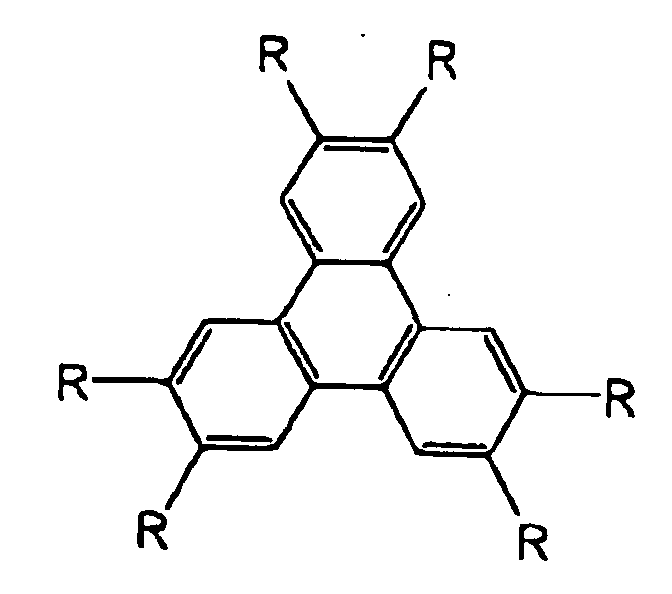
Examples of the discotic liquid crystals may
include triphenylene-type liquid crystals having
structures as shown below (as disclosed in Advanced
Materials, 1996, 8, No. 10). The below-indicated LC
Compounds 1 - 4 having side chains or substituents R
of alkoxy groups -OC
4H
9, -OC
5H
11 and -OC
6H
13 and a
thio-ether group -SC
6H
13 are known to exhibit a hole-transporting
performance at a high carrier mobility
(on the order of 10
-1 - 10
-3 cm/Vs). These compounds
exhibit a discotic columnar phase wherein disk-shaped
liquid crystal molecules are aligned to form a
columnar shape so that their triphenylene skeletons
rich in π-electrons are mutually superposed, thus
exhibiting a good hole-transporting characteristic via
the triphenylene group. LC Compound 5 shown below was
developed by our research group and, because of poly-fluorinated
side chains, exhibits a discotic liquid
crystal phase range shifted to a lower temperature
side and a lower ionization potential than the
corresponding non-fluorinated compound. LC Compound 7
has a dibenzopyrene skeleton and also exhibits a
discotic columnar phase.
- LC Compound 1:
- R=SC6H13
- LC Compound 2:
- R=OC4H9
- LC Compound 3:
- R=OC5H11
- LC Compound 4:
- R=OC6H13
- LC Compound 5:
- R=OC4H8C2F5
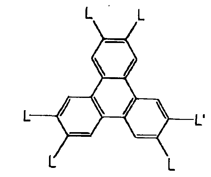
- LC Compound 6:
- L=OC5H11
- LC Compound 7:
- R=OC5H11
Other discotic liquid crystals may include
those having skeletons of phthalocyanine derivatives,
naphthalocyanine derivatives, truxene derivatives,
hexabenzocolonene derivatives and benzoquinone
derivatives.
Representative smectic liquid crystal
materials may include LC Compounds 8 - 11 shown below
(as disclosed in Applied Physics ("Ohyou Butsuri),
Vol. 68, No. 1, p. 26 - (1999)).
LC Compound 8
LC Compound 9
LC Compound 10
LC Compound 11
LC Compound 8 shown above classified as a
phenylbenzothiazole derivative and showing smectic A
phase has a hole-transporting characteristic. LC
Compound 9 classified as a phenylnaphthalene
derivative shows smectic A phase and smectic E phase
and a higher mobility in the smectic E phase of a
higher order than the smectic A phase, and also
exhibits bipolar carrier (i.e., hole and electron)-transporting
characteristic. LC Compounds 8 and 9
both show a high mobility of 10-3 cm/V.s or higher.
Other liquid crystal compounds having a bar-shaped
skeleton and showing a smectic liquid crystal
phase may also be used.
Such a liquid crystal compound, when used in
the electron- or hole-transporting layer 3 or 6 of the
structures shown in Figures 1A and 1B, is expected to
provide a device of an improved performance at a good
productivity.
The characteristics of a carrier-transporting
liquid crystal material may be summarized as (i) a
high carrier mobility due to self-alignment
characteristic in the bulk state and (ii) a high
carrier-injection characteristic due to a π-electron
conjugated plane aligned parallel to the electrode
boundary, which are not possessed by the conventional
materials.
We have further studied as to whether more
effective luminescence can be attained by generating
carriers in an organic layer in addition to carrier
injection from the electrodes. Hitherto, several
studies have been reported regarding the doping of a
carrier-transporting material with an electron-accepting
or electron-donating compound in an organic
layer, e.g., in (1) Applied Physics Letter, vol. 72,
No. 17, p. 2147 (1998) Yamamoto, et al., and (2)
Applied Physics Letter, vol. 73, No. 20, p. 2866
(1998) Kido, et al.
The above reference (1) reports that a
polymeric material constituting a hole-transporting
layer is doped with 20 mol. % of a salt containing
SbCl6 - so as to generate holes and increase the
carrier density in the hole-transporting polymeric
material, thereby succeeding in high luminance
emission. The above reference (2) reports an
improvement in electron injection performance by
doping an electron-transporting layer with Li metal.
Doping of liquid crystals has been reported,
e.g., in (3) J. Am. Chem. Soc., vol. 116, No. 23, p.
10808 (1994) Boden, et al., and (4) J. Material
Science: Materials in Electronics, 5, p. 83 (1994).
The above reference (3) reports that a
discotic liquid crystal material having a
tricycloquinazoline is doped with 6 mol. % of
potassium to provide an n-type semiconduction for
transporting electrons as a principal carrier. The
reference (4) reports that a discotic liquid crystal
material having a triphenylene skeleton is doped with
AlCl3 to provide a p-type semiconductor for
transporting holes as a principal carrier.
In the case where an electronic device
including a layer of liquid crystal material doped
with an inorganic material is supplied with an
external electric field, not only electronic carriers
(holes or electrons) but also ionic (anionic or
cationic) dopants are moved in the liquid crystal
layer under the external electric field, thus causing
an ionic current. The ionic current is caused by
movement of the dopants per se and thus results in a
poor reversibility of current characteristic, thus
leaving problems in not only initial performance but
also long-term performance. Particularly, in the case
of a liquid crystal material having a liquid
characteristic, the problem of the ionic current is
liable to be more serious than in the case of
amorphous or polymeric materials. The above-mentioned
references (3) and (4) were both directed to a device
including a liquid crystal layer alone of which the
voltage-current characteristic was measured as a basic
property, so that a serious problem was not believed
to be encountered even if an ionic current and an
electronic current were co-present.
SUMMARY OF THE INVENTION
In view of the above-mentioned problems, a
principal object of the present invention is to obtain
a liquid crystal composition by utilizing an effective
doping technique stably applicable to a liquid crystal
and provide a liquid crystal device capable of
constituting an electronic device showing good
performances by using the liquid crystal composition.
According to the present invention, there is
provided a liquid crystal device, comprising: a pair
of electrodes, and a plurality of layers disposed
between the electrodes and including at least one
liquid crystal layer which comprises a liquid crystal
composition having an electronic carrier-transporting
function and comprising at least two compounds
including at least one electron-donating compound or
electron-accepting compound having a π-electron
conjugated structure.
In the liquid crystal device according to the
present invention, the liquid crystal layer included
therein and having an electronic carrier transporting
function contains an electron-donating compound or
electron-accepting compound having a π-electron
conjugated structure, whereby carriers can be stably
formed by mutual interaction with another compound
therein. As a result, the liquid crystal is
effectively and stably doped to exhibit a good
electronic current characteristic. According to the
present invention, it becomes possible to realize an
electronic device, such as a semiconductor device or a
luminescence device exhibiting remarkably improved
performances.
These and other objects, features and
advantages of the present invention will become more
apparent upon a consideration of the following
description of the preferred embodiments of the
present invention taken in conjunction with the
accompanying drawings.
BRIEF DESCRIPTION OF THE DRAWINGS
Figures 1A and 1B are schematic sectional
views showing basic organizations of organic EL
devices.
Figure 2 is a schematic sectional view of a
MOS-type FET device including a liquid crystal device
structure of the invention.
Figure 3 is a schematic sectional view of a
diode including a liquid crystal device structure of
the invention.
Figures 4 and 5 are schematic sectional views
each showing an organization of an organic EL device.
DESCRIPTION OF THE PREFERRED EMBODIMENTS
The present invention aims at providing a
high-performance liquid crystal device by utilizing a
good current characteristic of a liquid crystal
attributed with a high degree of order resulting from a
self-alignment characteristic of the liquid crystal,
particularly by using a liquid crystal composition
comprising plural compounds.
The significance of using a liquid crystal
compound for constituting various semiconductors will
now be discussed to some extent in comparison with Si
crystal semiconductor. Si crystal has a band gap of
ca. 1.1 eV, and is generally doped with electron-donating
or electron-accepting atoms to increase the
density of electrons in the conduction band or holes
in the valence band, thus generating free carriers.
By using these techniques, various functional devices
are provided while adopting various combinations of pn-junctions,
etc.
On the other hand, a liquid crystal compound
generally has a band gap of 2 - 3 eV, and the density
of thermally excited free carriers is low. In the
case of an organic EL device operated by utilizing
externally injected electrons and holes as carriers, a
liquid crystal compound having a low density of free
carriers can be used, and a still higher efficiency
can be expected by doping the liquid crystal compound
so as to realize a higher current density and a higher
luminance.
Thus, in order to increase the utility of a
liquid crystal compound, an appropriate proportion of
an electron-donating or electron-accepting compound is
blended so as to provide a p-type or n-type
semiconductor in the present invention.
Figure 2 is a schematic sectional view of a
MOS (metal oxide semiconductor)-type FET (field effect
transistor) device using a liquid crystal layer as an
example of transistor including a liquid crystal
device structure of the present invention. Referring
to Figure 2, the device includes a gate electrode 21,
a gate insulating film 22, an organic active layer 23,
a drain electrode 24 and a source electrode 25. In
this device, the organic active layer 23 is formed of
a liquid crystal composition. The other members are
similar to the corresponding members in a conventional
MOS-type FET device. The liquid crystal composition
may constitute, e.g., an n-type semiconductor layer by
incorporating a certain proportion of electron-donating
compound. In this instance, a current is
caused to flow between the source 25 and the drain 24
when a positive voltage exceeding a threshold is
applied to the gate electrode 21.
Figure 3 is a schematic sectional view of an
example of diode including a liquid crystal device
structure of the present invention. Referring to
Figure 3, the diode includes electrodes 31 and 34,
between which a p-type semiconductor layer 32 and an
n-type semiconductor layer 33 are disposed. In this
device, the electrodes 31 and 34 are similar to those
in a conventional diode, and the p-type semiconductor
layer 32 and the n-type semiconductor layer 33 are
respectively formed of a liquid crystal composition by
incorporating an electron accepting compound in the p-type
semiconductor layer 32 and an electron-donating
compound in the n-type semiconductor layer 33. The
device shows a rectifying characteristic so that a
current flows in the case where a voltage is applied
between the electrodes 31 and 34 with the electrode 31
as a positive electrode.
In the liquid crystal device of the present
invention, a satisfactory performance cannot be
attained if impurities exceeding a certain level are
contained in the liquid crystal layer so as to
function as a carrier trap. Such impurities may
include organic by-products formed during the
synthesis of a liquid crystal compound, and can be
basically removed by re-crystallization and
sublimation for purification. It is indispensable to
reduce the impurity concentration to below a certain
level in order to provide a high-performance device.
Especially in the case of doping, the device
performance is greatly affected by a concentration of
impurities other than the dopant. Accordingly, in the
present invention, the impurity concentration of a
liquid crystal compound before the doping should be
suppressed to at most 1 wt. % as measured by high-performance
liquid chromatography (HPLC).
Dopants to be added to liquid crystal
compounds may be generally classified into inorganic
compounds and organic compounds (having a π-electron
conjugated structure), and the organic compounds are
used as the dopant in the present invention, inclusive
of an electron-donating compound having a low
ionization potential and an electron-accepting
compound having a large electron affinity.
More specifically, the liquid crystal
composition used in the present invention has an
electronic carrier-transporting function and comprises
at least two compounds including at least one compound
which is an electron-donating compound or an electron-accepting
compound respectively having a π-electron
conjugated compound.
The electron-donating compound may preferably
have an ionization potential IpD satisfying the
following relationship with an ionization potential
IpLC of another compound constituting the liquid
crystal composition:
IpD - IpIC < -0.3 eV.
On the other hand, the electron-accepting
compound may preferably have an ionization potential
IpA satisfying the following relationship with an
ionization potential IpLC of another compound
constituting the liquid crystal composition:
IpA - IpIC > 0.3 eV.
By using an electron-donating compound or an
electron-accepting compound satisfying the above
requirement, it becomes possible to stably generate
free carriers in the liquid crystal composition.
Specific examples of the electron-donating
compound and the electron-accepting compound usable in
the present invention are enumerated hereinbelow.
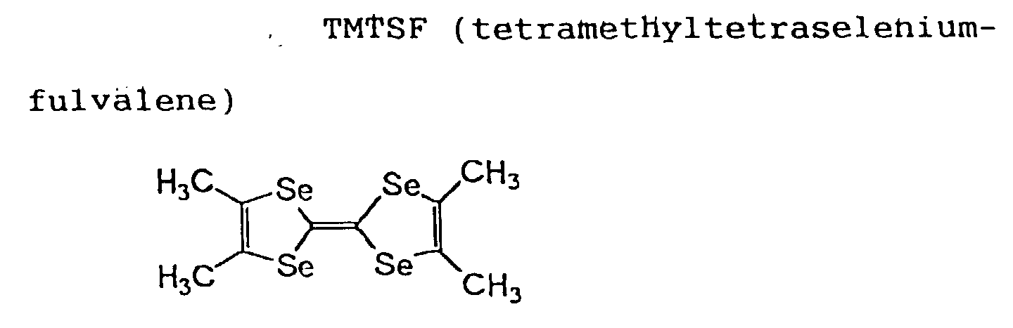
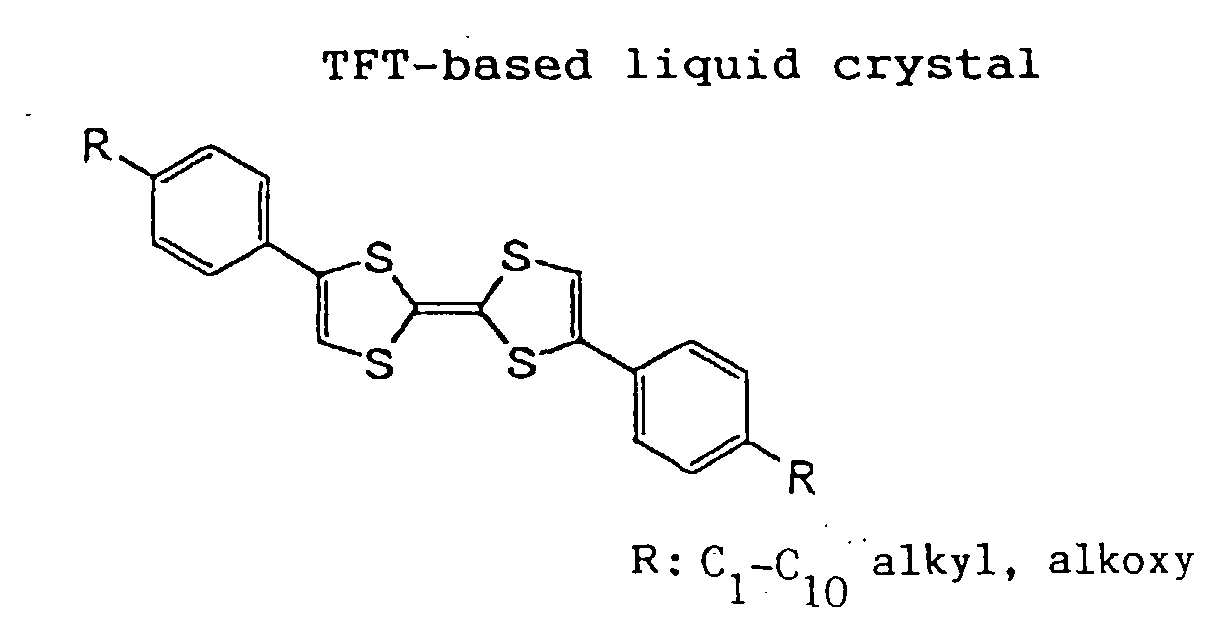
[Electron-donating compounds]
Compound 11: TTF (tetrathiafulvalene)
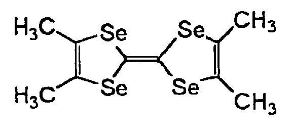
Compound 12: TMTSF (tetramethyltetraselenium-fulvalene)
Compound 13: TFT-based liquid crystal
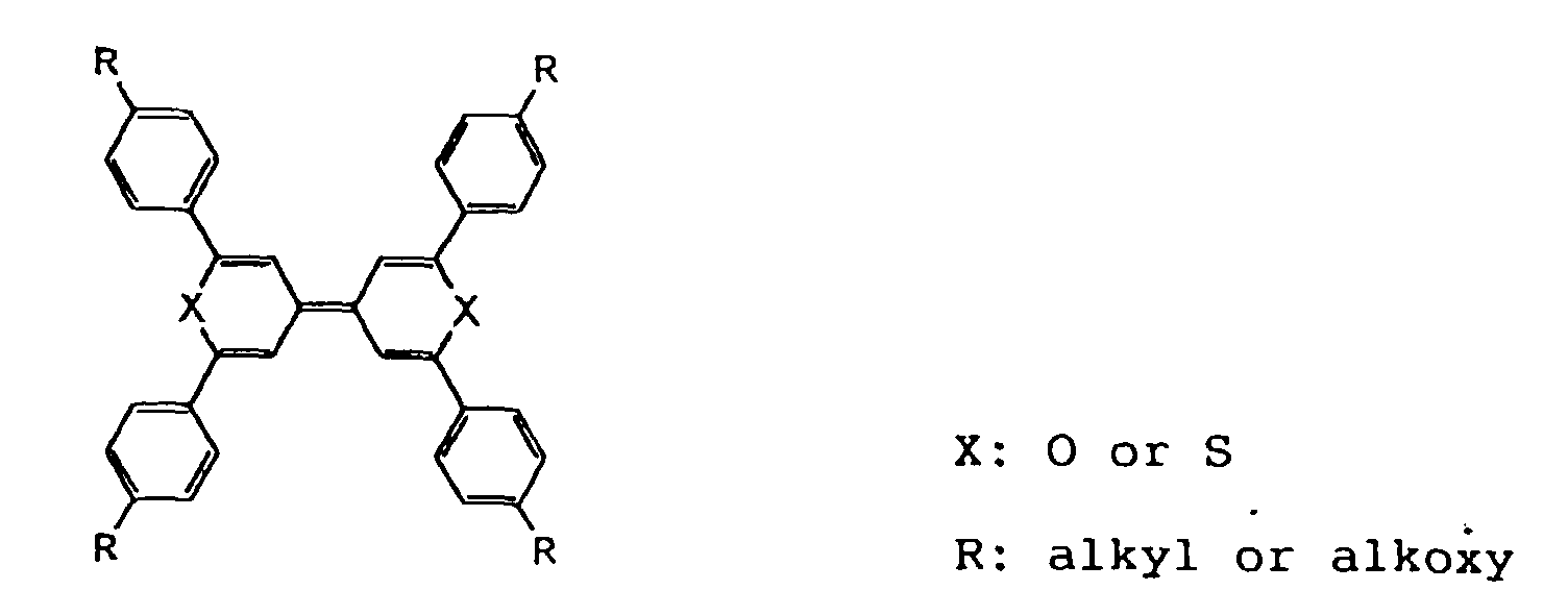
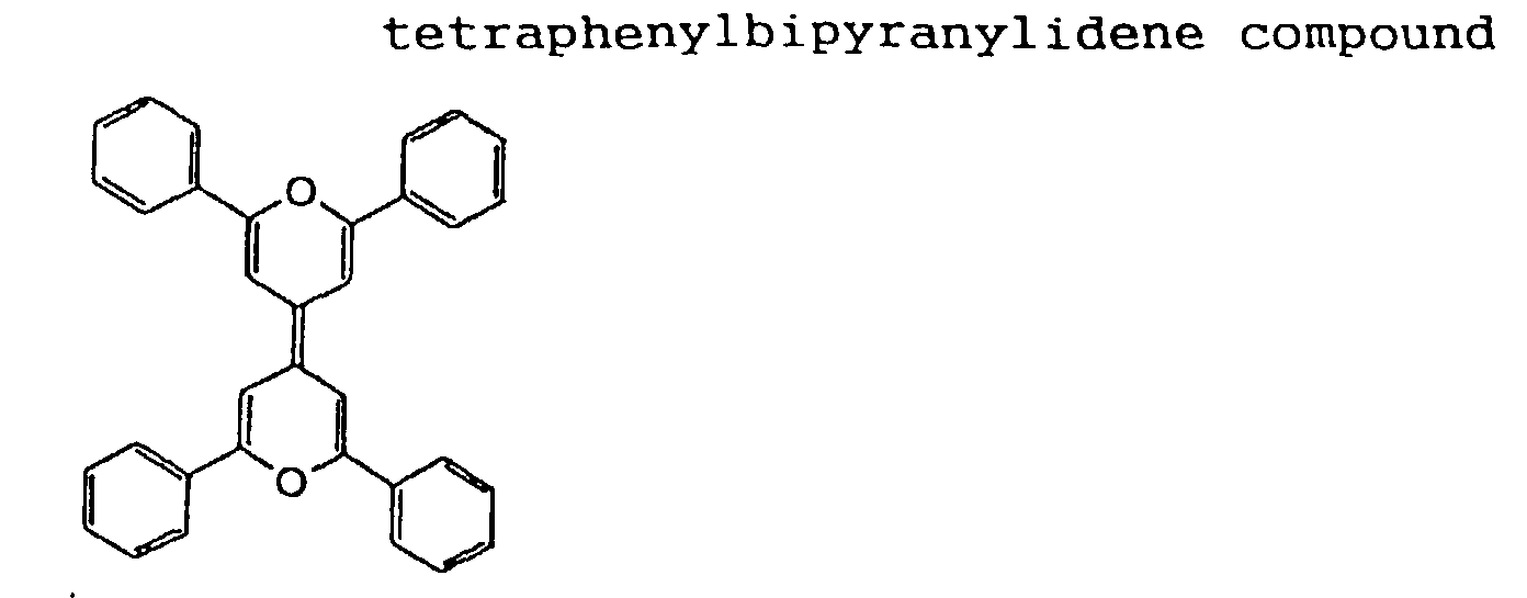
Compound 14: tetraphenylbipyranylidene compound
Compound 15: tetraphenylbipyranylidene-based liquid
crystal compound
[Electron-accepting compounds]
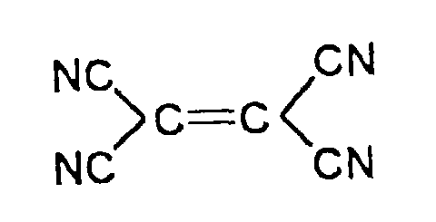
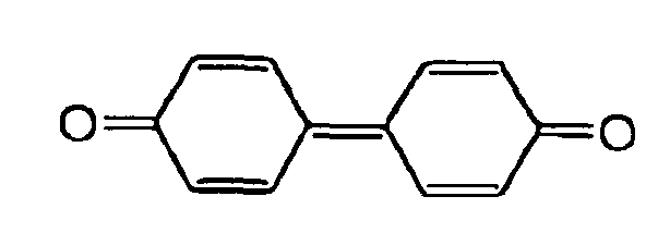
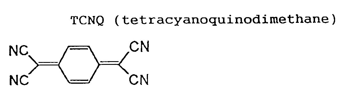
Compound 21: TCNQ (tetracyanoquinodimethane)
Compound 22: TCNE (tetracyanoethylene)
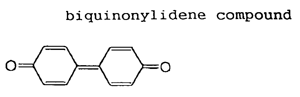
Compound 23: biquinonylidene compound
Compound 24: dithiolene-based nickel complex liquid
crystal compound
As mentioned above, the inorganic dopants
(inclusive of electron-donating materials comprising
metals, such as Li, Na, K and Cs, and electron-accepting
materials, such as Br2, I2, Cl2, BF3, PF5,
SbF5, SO3, FeCl3 and AlCl3) have only a relatively
small volume compared with the liquid crystal
compounds and the above-mentioned organic dopants.
Liquid crystal compound molecules are aligned in
stacked forms for their skeletons and side chains,
respectively. Accordingly, ionized small molecules of
such an inorganic dopant particularly present at the
side chains of the host liquid crystal molecules are
liable to move under an electric field, so that the
resultant ionic current cannot be negligible.
On the other hand, the organic dopants used
in the present invention have a molecular volume
comparable to or even larger than the volume of a
skeleton part of the host liquid crystal compound and
cause a charge transfer due to π-electron interaction,
to generate carriers. As a result, the host liquid
crystal and the dopant are bonded by a relatively
strong interaction to form a charge transfer complex.
Accordingly, an organic dopant is not liable to move,
thus resulting in only a negligible level of ionic
current and providing a durable and reliable device.
As the organic dopant, it is also possible to use a
liquid crystal compound as mentioned above.
Further, it is possible to form a more stably
functioning device by disposing a layer of compound
capable of transporting a species of carrier (holes or
electrons) identical to the principal species of
carrier transported by the doped liquid crystal layer
in lamination with the liquid crystal layer. The
additional layer functions as a protective layer for
preventing diffusion of the dopant. In the absence of
such a protective layer, the luminescence can be
obstructed as by obstruction of electron transfer,
e.g., due to diffusion of a doping electron-accepting
compound in a hole-transporting liquid crystal layer
to an electron-transporting compound to form a new
electron level. This problem can be obviated by
disposing such an identical species carrier-transporting
layer in lamination with the doped liquid
crystal layer.
As is well known, in a device using Si
crystal, such an Si crystal layer has to be formed by
strict crystal growth, and this is costly and poses a
serious difficulty in producing a large-area device.
The liquid crystal layer used in the liquid crystal
device of the present invention can be formed by co-vapor
deposition according to the vacuum deposition
process or by application according to spin coating due
to self-aligning characteristic and alignment order
of a liquid crystal close to that of a crystal,
therefore at a high productivity. Accordingly, a
high-performance electronic device can be realized at
a low cost. Moreover, as the self-alignment
characteristic allows easy production of a large-area
device, it becomes possible to prepare such a large-area
device that cannot be realized by using
conventional Si crystal.
Hereinbelow, the present invention will be
more specifically described with reference to Examples
and Comparative Examples.
Example 1
An organic EL device having an organization
as shown in Figure 4 (wherein identical numerals
represent identical layers as in Figure 1A) and
including a hole-injection layer 7 was prepared by
using a liquid crystal composition formed by doping LC
Compound 4 mentioned above with 1 mol. % of Compound
21 (TCNQ) as an electron-accepting dopant for the
hole-injection layer 7. The liquid crystal
composition, as well as LC Compound 4, exhibited a
phase transition from crystal phase to discotic
columnar disordered phase at ca. 65 °C on temperature
increase.
First of all, a glass substrate 5 coated with
a 70 nm-thick ITO film 4 was further coated with a 1
wt. % chloroform solution of the above liquid crystal
composition by spin coating at 1000 rpm for 20 sec,
followed by drying to form a 60 nm-thick liquid
crystal layer (hole injection layer) 7.
The hole injection layer 7 was further coated
with a 20 nm-thick hole-transporting amorphous layer 4
of aNPD and with a 50 nm-thick luminescence layer of
Alq3, respectively by vacuum deposition at a rate of
0.2 nm under resistance heating at a vacuum of at most
1.06x10⁻³ Pa. Further, thereon, a 10 nm-thick layer
of Al/1.8 wt. % Li alloy and a 100 nm-thick Al layer
were formed by vacuum deposition at a vacuum of at
most 1.06x10⁻³ Pa to form a cathode 1, thereby
providing an organic EL device as shown in Figure 4.
Comparative Example 1
An organic EL device having an organization
as shown in Figure 4 was prepared in the same manner
as in Example 1 except that a hole-injection layer 7
was formed of LC Compound 4 alone without the
electron-accepting dopant (Compound 21).
The above prepared devices of Example 1 and
Comparative Example 1 were supplied with a DC voltage
of 10 volts with the
ITO 4 as the anode at 30 °C
(crystal phase) and 70 °C (liquid crystal phase)
respectively, whereby the following current values
were exhibited.
| | 30°C | 70°C |
| Example 1 | 4 mA/cm2 | 30 mA/cm2 |
| Comparative Example 1 | 0.5 mA/cm 2 | 5 mA/cm2 |
The device of Example 1 exhibited improved
current characteristics due to spontaneous alignment
in the liquid crystal phase (30 °C → 70 °C) and also
free carrier generation by addition of the dopant.
The increase in current was accompanied with an almost
proportional increase in emission luminance. The
device of Example 1 also exhibited good and stable
luminescence in a continual current conduction
durability test in a nitrogen atmosphere.
Example 2
An organic EL device having a structure as
shown in Figure 1B was prepared in the following
manner.
A glass substrate 5 coated with a 70 nm-thick
ITO film 4 was further coated with a 50 nm-thick layer
3 of aNPD and a 40 nm-thick layer 2 of Alq3,
respectively by vacuum deposition. Further thereon, a
20 nm-thick layer 6 of liquid crystal composition
comprising LC Compound 5 and Compound 11 (TTF) as an
electron-donating dopant in a ratio of 200:1 was
formed by co-vacuum deposition under a condition
giving a thickness ratio of 200:1 by preliminary
separate vacuum deposition tests. Further thereon, a
cathode 1 of AlLi/Al laminate structure was formed by
vacuum deposition in the same manner as in Example 1.
Comparative Example 2
An organic EL device was prepared in the same
manner as in Example 2 except that an electron-transporting
layer 6 was formed of LC Compound 5
alone.
The above-prepared organic EL devices of
Example 2 and Comparative Example 2 were respectively
supplied with a DC voltage of 10 volts with the
ITO 5
as the anode, whereby the following current values
were measured.
| | 30°C |
| Example 2 | 8 mA/cm2 |
| Comparative Example 2 | 1.5 mA/cm2 |
Incidentally, the liquid crystal composition
and LC Compound 5 assumed smectic liquid crystal phase
at 30 °C as a supercooled state. As shown above, the
device of Example 2 having a liquid crystal layer with
a dopant exhibited a substantially better current
characteristic.
Example 3, Comparative Example 3
Organic EL devices were prepared in the same
manner as in Example 2 and Comparative Example 2,
respectively, except that the LC Compound 5 was
replaced by LC Compound 10.
The above-prepared organic EL devices of
Example 3 and Comparative Example 3 were respectively
supplied with a DC voltage of 10 volts with the
ITO 5
as the anode, whereby the following current values
were measured.
| | 30°C |
| Example 3 | 11 mA/cm2 |
| Comparative Example 3 | 2 mA/cm2 |
Incidentally, the liquid crystal composition
and LC Compound 10 assumed smectic liquid crystal
phase at 30 °C as a supercooled state. As shown
above, the device of Example 3 having a liquid crystal
layer with a dopant exhibited a substantially better
current characteristic.
Example 4, Comparative Example 4
Organic EL devices were prepared in the same
manner as in Example 2 and Comparative Example 2,
respectively, except that the LC Compound 5 was
replaced by LC Compound 11.
The above-prepared organic EL devices of
Example 4 and Comparative Example 4 were respectively
supplied with a DC voltage of 10 volts with the
ITO 5
as the anode, whereby the following current values
were measured.
| | 30°C |
| Example 4 | 6 mA/cm2 |
| Comparative Example 4 | 0.5 mA/cm2 |
Incidentally, the liquid crystal composition
and LC Compound 11 assumed smectic liquid crystal
phase at 30 °C as a supercooled state. As shown
above, the device of Example 4 having a liquid crystal
layer with a dopant exhibited a substantially better
current characteristic.
Example 5
Four types of organic EL devices were
prepared in the same manner as in Example 1 except
that LC Compound 4 as a principal component of the
liquid crystal composition having 4 different levels
of purities i.e., 98.2 wt. %, 98.8 wt. %, 99.2 wt. %
and 99.5 wt. %, respectively, was used.
A liquid crystal compound can have different
purities through different degrees of purification
after its synthesis. The above four levels of
purities were obtained by changing the conditions of
column chromatography and re-crystallization, and
measured by HPLC (high-performance liquid
chromatography) according to the following conditions.
In view of the synthesis process, it is
believed that substantially all the impurities
could be detected.
The four lots of LC Compound 4 having
different impurities were respectively doped with 1
mol. % of Compound 21 as an electron-accepting dopant
to respectively provide a hole-transporting layer.
The current values of the thus-prepared four
organic EL devices were measured under application of
a DC voltage of 10 volts at 70 °C. The results are
shown below corresponding to purities of
LC Compound
4.
| Purity | Current (at 70°C) |
| 98.2 (wt. %) | 5 (mA/cm2) |
| 98.8 | 7 |
| 99.2 | 30 |
| 99.5 | 26 |
The above results show that a liquid crystal
compound should have a purity of at least 99.0 wt. %
as measured by HPLC before it is doped with an
electron-donating or -accepting compound.
Incidentally, the liquid crystal compounds used in
Examples 1 - 4 all had purities of 99.5 wt. % or
higher.
Example 6
An organic EL device having an organization
as shown in Figure 5 further including an electron-injection
layer 8 between the luminescence layer 2 and
the cathode 1 in the device of Figure 4 (Example 1).
Thus, the procedure of Example 1 was repeated
up to the formation of the 50 nm-thick luminescence
layer of Alq3. Further thereon, a 20 nm-thick layer 8
of liquid crystal composition comprising LC Compound 5
and Compound 11 (TFT) as an electron-donating dopant
in a ratio of 200:1 was formed as an electron-injection
layer by co-vacuum deposition under a
condition giving a thickness ratio of 200:1 by
preliminary separate vacuum deposition tests. Further
thereon, a cathode 1 of AlLi/Al laminate structure was
formed by vacuum deposition in the same manner as in
Example 1.
The above-prepared device was supplied with a
DC voltage of 10 volts with the
ITO 4 as the anode at
30 °C and 70 °C similarly as in Example 1. The
measured current values are shown below in parallel
with those of Example 1.
| | 30°C | 70°C |
| Example 6 | 5 mA/cm2 | 50 mA/cm2 |
| Example 1 | 4 mA/cm2 | 30 mA/cm2 |
As shown above, the organic EL device of
Example 6 further including an electron-injection
layer 8 comprising a layer of liquid crystal doped
with an electron-donating dopant (Compound 11)
exhibited a further better current characteristic than
the device of Example 1.