EP1103060B1 - Method of manufacturing a light-absorbing matrix for a cathode-ray tube - Google Patents
Method of manufacturing a light-absorbing matrix for a cathode-ray tube Download PDFInfo
- Publication number
- EP1103060B1 EP1103060B1 EP99927154A EP99927154A EP1103060B1 EP 1103060 B1 EP1103060 B1 EP 1103060B1 EP 99927154 A EP99927154 A EP 99927154A EP 99927154 A EP99927154 A EP 99927154A EP 1103060 B1 EP1103060 B1 EP 1103060B1
- Authority
- EP
- European Patent Office
- Prior art keywords
- layer
- panel
- areas
- light
- matrix
- Prior art date
- Legal status (The legal status is an assumption and is not a legal conclusion. Google has not performed a legal analysis and makes no representation as to the accuracy of the status listed.)
- Expired - Lifetime
Links
- 239000011159 matrix material Substances 0.000 title claims description 70
- 238000004519 manufacturing process Methods 0.000 title claims description 12
- 239000010410 layer Substances 0.000 claims description 103
- 229920002120 photoresistant polymer Polymers 0.000 claims description 48
- 238000000034 method Methods 0.000 claims description 29
- 108091008695 photoreceptors Proteins 0.000 claims description 25
- 239000000243 solution Substances 0.000 claims description 25
- 239000002904 solvent Substances 0.000 claims description 19
- YXFVVABEGXRONW-UHFFFAOYSA-N Toluene Chemical compound CC1=CC=CC=C1 YXFVVABEGXRONW-UHFFFAOYSA-N 0.000 claims description 15
- 238000000151 deposition Methods 0.000 claims description 10
- 239000007788 liquid Substances 0.000 claims description 8
- 239000002245 particle Substances 0.000 claims description 8
- 239000000049 pigment Substances 0.000 claims description 8
- XLYOFNOQVPJJNP-UHFFFAOYSA-N water Substances O XLYOFNOQVPJJNP-UHFFFAOYSA-N 0.000 claims description 8
- 239000011248 coating agent Substances 0.000 claims description 7
- 238000000576 coating method Methods 0.000 claims description 7
- 239000000725 suspension Substances 0.000 claims description 7
- XMGQYMWWDOXHJM-JTQLQIEISA-N (+)-α-limonene Chemical compound CC(=C)[C@@H]1CCC(C)=CC1 XMGQYMWWDOXHJM-JTQLQIEISA-N 0.000 claims description 6
- 239000011241 protective layer Substances 0.000 claims description 6
- 239000000203 mixture Substances 0.000 claims description 5
- 230000005855 radiation Effects 0.000 claims description 5
- NTIZESTWPVYFNL-UHFFFAOYSA-N Methyl isobutyl ketone Chemical compound CC(C)CC(C)=O NTIZESTWPVYFNL-UHFFFAOYSA-N 0.000 claims description 4
- 238000007599 discharging Methods 0.000 claims description 4
- KHIWWQKSHDUIBK-UHFFFAOYSA-N periodic acid Chemical compound OI(=O)(=O)=O KHIWWQKSHDUIBK-UHFFFAOYSA-N 0.000 claims description 4
- 239000007864 aqueous solution Substances 0.000 claims description 3
- LNOPIUAQISRISI-UHFFFAOYSA-N n'-hydroxy-2-propan-2-ylsulfonylethanimidamide Chemical compound CC(C)S(=O)(=O)CC(N)=NO LNOPIUAQISRISI-UHFFFAOYSA-N 0.000 claims description 3
- 239000011253 protective coating Substances 0.000 claims 3
- 238000001035 drying Methods 0.000 claims 2
- 230000001681 protective effect Effects 0.000 claims 1
- OAICVXFJPJFONN-UHFFFAOYSA-N Phosphorus Chemical compound [P] OAICVXFJPJFONN-UHFFFAOYSA-N 0.000 description 11
- KFZMGEQAYNKOFK-UHFFFAOYSA-N Isopropanol Chemical compound CC(C)O KFZMGEQAYNKOFK-UHFFFAOYSA-N 0.000 description 8
- 238000010894 electron beam technology Methods 0.000 description 7
- 239000002131 composite material Substances 0.000 description 6
- 230000000717 retained effect Effects 0.000 description 5
- 230000005540 biological transmission Effects 0.000 description 4
- 239000011521 glass Substances 0.000 description 4
- OKKJLVBELUTLKV-UHFFFAOYSA-N Methanol Chemical compound OC OKKJLVBELUTLKV-UHFFFAOYSA-N 0.000 description 3
- UIHCLUNTQKBZGK-UHFFFAOYSA-N Methyl isobutyl ketone Natural products CCC(C)C(C)=O UIHCLUNTQKBZGK-UHFFFAOYSA-N 0.000 description 3
- 239000004372 Polyvinyl alcohol Substances 0.000 description 3
- 239000000463 material Substances 0.000 description 3
- 229920002451 polyvinyl alcohol Polymers 0.000 description 3
- 229910052724 xenon Inorganic materials 0.000 description 3
- FHNFHKCVQCLJFQ-UHFFFAOYSA-N xenon atom Chemical compound [Xe] FHNFHKCVQCLJFQ-UHFFFAOYSA-N 0.000 description 3
- SJEBAWHUJDUKQK-UHFFFAOYSA-N 2-ethylanthraquinone Chemical compound C1=CC=C2C(=O)C3=CC(CC)=CC=C3C(=O)C2=C1 SJEBAWHUJDUKQK-UHFFFAOYSA-N 0.000 description 2
- OKTJSMMVPCPJKN-UHFFFAOYSA-N Carbon Chemical compound [C] OKTJSMMVPCPJKN-UHFFFAOYSA-N 0.000 description 2
- KRHYYFGTRYWZRS-UHFFFAOYSA-N Fluorane Chemical compound F KRHYYFGTRYWZRS-UHFFFAOYSA-N 0.000 description 2
- 230000007423 decrease Effects 0.000 description 2
- 230000001419 dependent effect Effects 0.000 description 2
- 230000001678 irradiating effect Effects 0.000 description 2
- QSHDDOUJBYECFT-UHFFFAOYSA-N mercury Chemical compound [Hg] QSHDDOUJBYECFT-UHFFFAOYSA-N 0.000 description 2
- 229910052753 mercury Inorganic materials 0.000 description 2
- 239000002356 single layer Substances 0.000 description 2
- 239000004094 surface-active agent Substances 0.000 description 2
- VHQGURIJMFPBKS-UHFFFAOYSA-N 2,4,7-trinitrofluoren-9-one Chemical compound [O-][N+](=O)C1=CC([N+]([O-])=O)=C2C3=CC=C([N+](=O)[O-])C=C3C(=O)C2=C1 VHQGURIJMFPBKS-UHFFFAOYSA-N 0.000 description 1
- KGIGUEBEKRSTEW-UHFFFAOYSA-N 2-vinylpyridine Chemical compound C=CC1=CC=CC=N1 KGIGUEBEKRSTEW-UHFFFAOYSA-N 0.000 description 1
- 229910001209 Low-carbon steel Inorganic materials 0.000 description 1
- CTQNGGLPUBDAKN-UHFFFAOYSA-N O-Xylene Chemical compound CC1=CC=CC=C1C CTQNGGLPUBDAKN-UHFFFAOYSA-N 0.000 description 1
- 239000004793 Polystyrene Substances 0.000 description 1
- 229920004890 Triton X-100 Polymers 0.000 description 1
- 230000001464 adherent effect Effects 0.000 description 1
- XAGFODPZIPBFFR-UHFFFAOYSA-N aluminium Chemical compound [Al] XAGFODPZIPBFFR-UHFFFAOYSA-N 0.000 description 1
- 229910052782 aluminium Inorganic materials 0.000 description 1
- 230000015572 biosynthetic process Effects 0.000 description 1
- 229910052799 carbon Inorganic materials 0.000 description 1
- 239000003518 caustics Substances 0.000 description 1
- 239000003086 colorant Substances 0.000 description 1
- 238000007796 conventional method Methods 0.000 description 1
- 230000002950 deficient Effects 0.000 description 1
- 230000008021 deposition Effects 0.000 description 1
- 238000010586 diagram Methods 0.000 description 1
- 125000000664 diazo group Chemical group [N-]=[N+]=[*] 0.000 description 1
- 230000005686 electrostatic field Effects 0.000 description 1
- 238000005530 etching Methods 0.000 description 1
- 238000011010 flushing procedure Methods 0.000 description 1
- 229910002804 graphite Inorganic materials 0.000 description 1
- 239000010439 graphite Substances 0.000 description 1
- 230000005484 gravity Effects 0.000 description 1
- 238000007654 immersion Methods 0.000 description 1
- 239000012212 insulator Substances 0.000 description 1
- 230000033001 locomotion Effects 0.000 description 1
- 230000003278 mimic effect Effects 0.000 description 1
- 230000000737 periodic effect Effects 0.000 description 1
- 230000002093 peripheral effect Effects 0.000 description 1
- 229920002223 polystyrene Polymers 0.000 description 1
- 239000011347 resin Substances 0.000 description 1
- 229920005989 resin Polymers 0.000 description 1
- 239000002002 slurry Substances 0.000 description 1
- 239000007787 solid Substances 0.000 description 1
- 239000011877 solvent mixture Substances 0.000 description 1
- 239000000126 substance Substances 0.000 description 1
- JLZUZNKTTIRERF-UHFFFAOYSA-N tetraphenylethylene Chemical compound C1=CC=CC=C1C(C=1C=CC=CC=1)=C(C=1C=CC=CC=1)C1=CC=CC=C1 JLZUZNKTTIRERF-UHFFFAOYSA-N 0.000 description 1
- 238000005406 washing Methods 0.000 description 1
- 239000008096 xylene Substances 0.000 description 1
Images


Classifications
-
- H—ELECTRICITY
- H01—ELECTRIC ELEMENTS
- H01J—ELECTRIC DISCHARGE TUBES OR DISCHARGE LAMPS
- H01J9/00—Apparatus or processes specially adapted for the manufacture, installation, removal, maintenance of electric discharge tubes, discharge lamps, or parts thereof; Recovery of material from discharge tubes or lamps
- H01J9/20—Manufacture of screens on or from which an image or pattern is formed, picked up, converted or stored; Applying coatings to the vessel
- H01J9/22—Applying luminescent coatings
- H01J9/227—Applying luminescent coatings with luminescent material discontinuously arranged, e.g. in dots or lines
-
- H—ELECTRICITY
- H01—ELECTRIC ELEMENTS
- H01J—ELECTRIC DISCHARGE TUBES OR DISCHARGE LAMPS
- H01J29/00—Details of cathode-ray tubes or of electron-beam tubes of the types covered by group H01J31/00
- H01J29/02—Electrodes; Screens; Mounting, supporting, spacing or insulating thereof
- H01J29/10—Screens on or from which an image or pattern is formed, picked up, converted or stored
- H01J29/18—Luminescent screens
- H01J29/30—Luminescent screens with luminescent material discontinuously arranged, e.g. in dots, in lines
- H01J29/32—Luminescent screens with luminescent material discontinuously arranged, e.g. in dots, in lines with adjacent dots or lines of different luminescent material, e.g. for colour television
- H01J29/327—Black matrix materials
-
- H—ELECTRICITY
- H01—ELECTRIC ELEMENTS
- H01J—ELECTRIC DISCHARGE TUBES OR DISCHARGE LAMPS
- H01J9/00—Apparatus or processes specially adapted for the manufacture, installation, removal, maintenance of electric discharge tubes, discharge lamps, or parts thereof; Recovery of material from discharge tubes or lamps
- H01J9/20—Manufacture of screens on or from which an image or pattern is formed, picked up, converted or stored; Applying coatings to the vessel
- H01J9/22—Applying luminescent coatings
- H01J9/227—Applying luminescent coatings with luminescent material discontinuously arranged, e.g. in dots or lines
- H01J9/2278—Application of light absorbing material, e.g. between the luminescent areas
Definitions
- This invention relates to a method of manufacturing a light-absorbing matrix for a cathode-ray tube (CRT) and, more particularly to a method of making a matrix using a color selection electrode having openings substantially greater in width than the width of the resultant matrix openings.
- CTR cathode-ray tube
- Fig. 1 shows a shadow mask 2 and a viewing faceplate 18 of a conventional CRT screen surface having a screen assembly 22 thereon.
- the shadow mask 2 includes a plurality of slits, or rectangular openings, 4 only one of which is shown.
- the screen assembly 22 includes a light-absorbing matrix 23 with rectangular openings in which blue-, green-, and red-emitting phosphor lines, P b , P g and P r , respectively, are disposed.
- Three color-emitting phosphors and the matrix lines, or guardbands, therebetween comprise a triad having a width, or screen pitch, T , of about 0.84 mm (33 mils).
- the guardbands are designated hereinafter as RB, for the guardbands between the red- and blue-emitting phosphor lines; RG, for the guardbands between the red- and green-emitting phosphor lines; and BG, for the guardbands between the blue- and green-emitting phosphor lines.
- the mask openings 4 have a width, a, not greater than one third the width, T, of the triad. In a CRT having a diagonal dimension of 51 cm (20 inches), the width, a , of the shadow mask openings 4 are on the order of about 0.23 mm (9 mils) and the resultant openings formed in the matrix have a width, c , of about 0.18 mm (7 mils).
- the guardbands of the matrix 23, between the adjacent phosphor lines, have a width, d , of about 0.1 mm (4 mils).
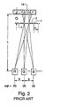
- the matrix 23, preferably, is formed on the viewing faceplate 18 by the process described in U.S. Pat. No. 3,558,310, issued to Mayaud on Jan. 26, 1971. Briefly, a film of a suitable photoresist, whose solubility is altered by light, is provided on the interior surface of the viewing faceplate 18. The photoresist film is exposed, through the openings 4 in the shadow mask 2, to ultraviolet light from a conventional three-in-one lighthouse, shown schematically in Fig. 2.
- the photoresist film is exposed sequentially and equally (6 exposures units (wgt) each, for example) by each of the light sources.
- the "G" source lies on the symmetry axis of the screen and mask.
- the regions of the photoresist film with greater solubility are removed by flushing the exposed film with water, thereby uncovering bare areas of the faceplate.
- the interior surface of the faceplate panel is overcoated with a black matrix slurry, of the type known in the art, which, when dried, is adherent to the uncovered areas of the faceplate.
- the matrix material overlying the retained film regions, as well as the retained film regions are removed, leaving the matrix guardbands on the previously uncovered areas of the faceplate panel.
- the positions on the screen surface denoted by b, g and r in Fig. 2 are the centers of the projected slit images.
- the difference between the width, a , of the shadow mask openings and the width, c , of the matrix openings is referred to as "print down.”
- the typical "print down" is about 0.05 mm (2 mils).
- a drawback of the shadow mask-type CRT is that, at the center of the screen, the shadow mask intercepts all but about 18 - 22 % of the electron beam current; that is, the shadow mask is said to have a transmission of only about 18 - 22 %.
- the area of the openings 4 in the shadow mask 2 is about 18 - 22 % of the area of the mask. Because there are no focusing fields associated with the shadow mask 2, a corresponding portion of the screen assembly 22 is excited by the electron beams.
- a post-deflection focusing color selection structure In order to increase the transmission of the color selection electrode without increasing the size of the excited portions of the screen, a post-deflection focusing color selection structure is required.
- the focusing characteristics of such a structure permit larger aperture openings to be utilized to obtain greater electron beam transmission than can be obtained with the conventional shadow mask.
- a uniaxial tension focus mask is described in U.S. Patent No. 5,646,478 issued to R. W. Nosker et al. on July 8, 1997.
- a drawback of using a post deflection color selection electrode, such as a tension focus mask is that conventional methods for forming the matrix cannot be utilized, because the prior methods provide only about a 0.05 mm (2 mil) "print down."
- the triad period or pitch, T of the screen assembly is the same as for a CRT with a conventional shadow mask, so the matrix openings are about 0.18 mm wide.
- a "print down" of about 0.37 mm (14.5 mils) is required. Such a high degree of "print down” cannot be achieved with the conventional matrix process described above.
- any matrix opening patterns formed using a conventional three-in-one lighthouse process such as that taught by Mayaud, referenced above, will result in misregister of the electron beams which impinge upon the blue- and red-emitting phosphors and also nonparity of the intratrio openings with "Q"-space errors.
- "Q"-space errors of the order of +/- 5% that is variations in the focus mask-to-screen spacing caused by deviations of the faceplate thickness or curvature from the bogie dimensions, are typical. Accordingly, a new method of making a matrix with the capability for very large "print down" is required.
- GB-A-2 307 094, dated May 14, 1997 describes a method of making a matrix, comprising coating a conductive layer on the inner surface of a color CRT panel, overcoating a photoconductive layer on the conductive layer, establishing an electrostatic charge on the photoconductive layer, exposing selected areas of the photoconductive layer, and developing the exposed panel.
- the developing may non-preferably be by a dry electrophotographic method, wherein a black matrix is said to be fixed by irradiating infrared rays from an IR lamp on the panel.
- the developing may preferably be by a wet electrophotographic method, employing a solution of light-absorptive material, wherein a residual solution on the developed panel is removed and the light-absorptive material is fixed on the panel.
- the method described does not make a matrix with the capability for very large "print down.”
- the present invention relates to a method of manufacturing a light-absorbing matrix, having a plurality of openings formed therein, on an interior surface of a faceplate panel of a cathode-ray tube.
- a photoreceptor having a plurality of layers including a photoresist layer, a conductive layer, and a photoconductive layer, is formed on the interior surface of the panel and electrostatically charged to a substantially uniform level of charge.
- a color selection electrode having a plurality of openings, substantially greater in a dimension than the corresponding openings in the light-absorbing matrix, is inserted into the panel.
- the photoreceptor is exposed to light through the openings in the color selection electrode to selectively discharge the more intensely illuminated areas of the photoreceptor, without substantially discharging the less intensely illuminated areas and without substantially irradiating the underlying photoresist.
- the color selection electrode is removed from the panel after the exposure step, and the photoreceptor is contacted with a suitable liquid toner to form toner lines.
- the liquid toner comprises pigment particles having a charge opposite in polarity to the charge on the less intensely illuminated areas of the photoreceptor.
- the color selection electrode is re-inserted into the panel and the photoreceptor is exposed to UV radiation to selectively change the solubility of the photoresist layer thereof, thus creating areas of greater solubility underlying the toner lines and areas of lesser solubility therebetween.
- the photoreceptor is serially developed to remove the areas with lesser solubility and expose portions of the interior surface of the panel, while leaving intact the areas of lesser solubility.
- the exposed portions of the interior surface of the panel and the areas of lesser solubility are coated with a matrix suspension and dried to form a matrix.
- the matrix is developed by contacting it with a solvent to remove the areas of lesser solubility and the overlying light-absorbing matrix thereon, without removing the light-absorbing matrix from the exposed portions of the interior surface of the panel.
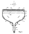
- Fig. 3 shows a cathode-ray tube 10 having a glass envelope 11 comprising a rectangular faceplate panel 12 and a tubular neck 14 connected by a rectangular funnel 15.
- the funnel has an internal conductive coating (not shown) that extends from an anode button 16 to the neck 14.
- the panel 12 comprises a cylindrical viewing faceplate 18 and a peripheral flange or sidewall 20 that is sealed to the funnel 15 by a glass frit 17.
- a three-color phosphor screen 22 is carried by the inner surface of the faceplate 18.
- the screen 22 is a line screen with the blue-, green-, and red-emitting phosphors arranged in triads, each triad including a phosphor line of each of the three colors, P b , P g and P r , separated by opaque lines of a light-absorbing matrix 23, shown in Fig. 4.
- a cylindrical multi-apertured color selection electrode, such as a tension focus mask, 24 is removably mounted within the panel 12, in predetermined spaced relation to the screen 22.
- An electron gun 26, shown schematically by the dashed lines in Fig. 3, is centrally mounted within the neck 14 to generate and direct three inline electron beams (also not shown) along convergent paths through the tension focus mask 24 to the screen 22.
- the electron gun is conventional and may be any suitable gun known in the art.
- the CRT 10 is designed to be used with an external magnetic deflection yoke, such as the yoke 30, shown in the neighborhood of the funnel-to-neck junction.
- the yoke 30 subjects the three beams to magnetic fields that cause the beams to scan a horizontal and vertical rectangular raster over the screen 22.
- an aluminum layer (not shown) overlies the screen 22 and provides an electrical contact thereto, as well as a reflective surface to direct light, emitted by the phosphors, outwardly through the viewing faceplate 18.
- the tension focus mask 24 is formed, preferably, from a thin rectangular sheet of about 0.05 mm (2 mil) thick low carbon steel, that includes two long sides and two short sides.
- the tension focus mask 24 includes an apertured portion that contains a plurality of first elongated strands 32 separated by slots 33 that parallel the minor axis, Y, of the mask.
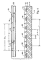
- the mask pitch, D m defined as the transverse dimension of a first strand 32 and an adjacent slot 33, is 0.85 mm (33.5 mils).
- each of the first strands 32 has a transverse dimension, or width, w , of about 0.39 mm (15.5 mils) and each of the slots 33 has a width, a ', of about 0.46 mm (18 mils).
- the slots 33 extends from near one long side of the tension focus mask to near the other long side thereof.
- a plurality of second strands 34 are disposed substantially parallel to the first strands 32 and spaced therefrom by insulators 36.
- the frame 38 comprises four major members: two torsion members 40 and 41; and two side members 42 and 43. The two torsion members, 40 and 41, parallel the major axis, X, and each other.
- the screen 22, formed on the viewing faceplate 18, includes the light-absorbing matrix 23 with rectangular openings in which the color emitting phosphor lines are disposed.
- the corresponding matrix openings have a width, c, of about 0.25 mm (6.1 mils).
- the width, d , of each matrix line is about 0.15 mm (5.8 mils) and each phosphor triad has a width or screen pitch, T , of about 0.91 mm (35.8 mils).
- the tension focus mask 24 is spaced at a distance, Q, (hereinafter Q-spacing) of about 15.24 mm (600 mils) from the center of the interior surface of the faceplate panel 12.
- Q a distance between the first strands 32 and the second strands 34, at an anode voltage of 30 kV, is about 800 volts.
- the pitch, D m of the tension focus mask 24 can be varied.
- the corresponding screen pitch, T is 0.68 mm (26.78 mils).
- Each matrix opening has a width, c, of about 0.11 mm (4.5 mils) and a matrix line width, d , of about 0.11 mm (4.5 mils).
- the voltage difference between the first strands 32 and the second strands 34, at an anode voltage of 30 kV is about 750 volts.
- the corresponding screen pitch, T is 0.42 mm (16.5 mils).
- Each matrix opening has a width, c, of about 0.051 mm (2 mils) and a matrix line width, d, of about 0.089 mm (3.5 mils).
- the voltage difference between the first strands 32 and the second strands 34, at an anode voltage of 30 kV is about 650 volts.
- the method of manufacturing the matrix 23 will be described in an embodiment using the tension focus mask 24 with a mask pitch, D m , of 0.68 mm as a photographic master.
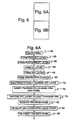
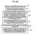
- the panel 12 is cleaned, as indicated in step 50 of Fig. 6, by washing it with a caustic solution, rinsing it in water, etching it with buffered hydrofluoric acid and rinsing it again with water, as is known in the art.
- the interior surface of the viewing faceplate 18 of the panel 12 is then coated with a polyvinyl alcohol (PVA) solution and dried to form a precoat layer 54, shown in Fig. 7.
- PVA polyvinyl alcohol
- the precoat layer 54 provides a uniform surface condition for the deposition for subsequent materials.
- the thickness of the precoat layer 54 is on the order of a monolayer.
- a negative photoresist solution is overcoated onto the precoat layer 54 and dried to form a photoresist layer 56, as indicated in step 58.
- the photoresist solution comprises 1.08 wt. % of PVA; 1.08 wt. % PVP; 0.6 wt. % of a sensitizer, such as Diazo Resin #8, available from Fairmount Chemical Co., Inc., Newark, NJ; 0.02 wt.
- the photoresist layer 56 has a thickness of about 1 ⁇ 0.2 ⁇ m.
- an organic conductive solution is overcoated onto the photoresist layer 56 and dried to form an organic conductive (OC) layer 62, as indicated in step 60.
- the thickness of the OC layer 62 is about 1 ⁇ 0.2 ⁇ m.
- the OC solution comprises about 0.62 wt. % PVP; 5.84 wt. % MS-905, available from BASF, Parsippany, NJ.; and the balance, methanol.
- an organic photoconductive solution is provided to overcoat the OC layer 62 and dried to form an organic photoconductive layer (OPC) 66.
- the OPC layer 66 has a thickness of about 5 ⁇ 1 ⁇ m.
- the OPC solution comprises about 0.005 wt. % of the surfactant UL-7602, available from Union Carbide, Danbury, CT; about 0.23 wt. % of 2,4,7-trinitro-9-fluorenone (TNF); about 0.35 wt. % of 2-ethylanthraquinone (EAQ); about 2.32 wt. % of tetraphenylethylene (TPE); about 9.28 wt.
- the surfactant UL-7602 available from Union Carbide, Danbury, CT
- TNF 2,4,7-trinitro-9-fluorenone
- EAQ 2-ethylanthraquinone
- TPE tetraphenylethylene
- % polystyrene about 24.49 wt. % xylene; and the balance, toluene.
- a poly-2-vinylpyridine (PVPy) solution is applied to overcoat the OPC layer 66 and dried to form a protective layer 70, having a thickness of about 0.7 ⁇ 0.2 ⁇ m.
- the photoresist layer 56, the OC layer 62 and the OPC layer 66 are referred to hereinafter, collectively, as the photoreceptor 72.
- the faceplate panel is then placed on a charging apparatus of the type described in U.S. 5,519,217, issued to Wilbur et al., on May 21, 1996, and the OPC layer 66 of the photoreceptor 72 is electrostatically charged to a positive voltage of 425 ⁇ 25V to provide a substantially uniform level of charge, as indicated in step 74.
- the tension focus mask 24 is inserted into the faceplate panel 12 and mounted within a lighthouse, containing a plurality of light sources.
- CRT's embodying the tension focus mask 24 may have an opening a' with a width between D m /3 and 2D m /3. If one were to use the three light sources, R, G and B, shown in Fig. 2, to project an image of the mask openings 33 of Fig. 4, significant spatial overlap at the screen would occur. The result would be that the area of least exposure would be centered on the projected image of the opening 33, where it is intended that one of the phosphor stripes would eventually be centered. To avoid this problem all of the light source positions of Fig.
- the light source geometries for the exposure procedures for a conventional CRT with a shadow mask and a CRT using a tension focus mask 24, are summarized as entries 1 - 3 of the TABLE.
- the TABLE indicates the light source locations and exposure weights (in parenthesis).
- column 1 indicates the light locations and exposure weights for the conventional CRT and shadow mask of Fig. 2.
- Column 2 represents a CRT using the tension focus mask 24 with the light locations left shifted, and column 3 represents the same tension focus mask 24 with the light locations right shifted.
- the values of s used to set the locations of the light sources in a lighthouse are linked to the design values L, D m , and Q o .
- the lateral shift of the light sources required for printing screens for a CRT having a tension focus mask 24 affects only the reference position of the matrix stripes with respect to the mask openings 33.
- Equation 4 provides a description of the center of the individual exposure profiles for a given source position.
- the equation is a very good approximation for the tension focus mask system, i.e., diffraction has little influence on the accuracy of the equation.
- Grouping or degrouping of a triad will be influenced by the summation of the exposure patterns; however, for a tension focus mask system with "Q" errors, the center of the individual exposure profiles described by equation 4 do not track the resultant grouping of degrouping.
- the exposure sequence taught by the entry in column 8 of the TABLE yields grouping with short "Q" that is less severe than one may expect from equation 4 and, likewise, the degrouping with long "Q" is less severe than may expect from equation 4.
- Grouping refers to the tendency of the red and blue triad centers to move toward the green center with short Q-error (i.e., b, g and g, r ⁇ T / 3 in Fig. 3).
- Degrouping refers to the tendency of the red and blue triad centers to move away from the green center with long Q-error (i.e., b, g and g, r > T / 3 in Fig. 2).
- equation (5) states that the fractional image shifts for a given Q-error are twice as large as in equation (4), and are in the opposite directions.
- the projected red and blue slit images experience twice the weight from the B and R source locations as from the R' and B' source locations. Additionally, the composite image, contributed by all light sources associated with a given color, receives the same total exposures of six units, as in the conventional practice.
- the motions of the red-image and the blue-image centroids from the weighted type 1 and type 2 exposures cancel each other in the combined exposure.
- the contrast level of the composite red or blue image decreases somewhat, but the peak location and exposure width remain relatively fixed, and exhibit acceptably small errors.
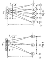
- Fig. 9 illustrates the composite exposure procedure that minimizes the matrix stripe grouping or de-grouping problems resulting from small Q-spacing errors.
- the composite exposure pattern assigns relative exposure weights of two units from B', four units from R, six units from G, four units from B, and two units from R'.
- the procedure is summarized in column 5 of the TABLE.
- the lateral shift of the light sources required for the CRT having the tension focus mask 24 affects only the reference position of the matrix stripes with respect to the mask slits or openings 33, and has no influence on the matrix opening parity.
- Matrix opening parity refers to the condition in which the matrix openings in a given triad are equal in width. Consequently, shifting the array of the five light sources in Fig. 9 by a lateral distance of s /2, as summarized for a left shift in column 6 of the TABLE minimizes the grouping problem, for a CRT having a tension focus mask, in the presence of Q-errors.
- the mask-screen symmetry axis lies midway between light sources G and B.
- the exposure pattern may be shifted right by a lateral distance s /2 for the same tube type, as summarized in column 7 of the TABLE.
- the weighted 5-position exposure significantly aids in compensating for stripe-to-stripe spacing errors, and is found adequate for this purpose in the screen fabrication process for CRT having a tension focus mask.
- the overall exposure directions in the lighthouse are not symmetrical about the normal to the screen center, which is also the symmetry axis for the in-line electron gun assembly of the CRT.
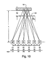
- a 6-position composite exposure which exhibits such symmetry about the electron gun and screen axis can be obtained by halving the weights of the light sources in the exposures of columns 6 and 7 of the TABLE, and combining the two sequences. The results are shown in Fig. 10 and summarized in column 8 of the TABLE.
- a xenon light source within the lighthouse exposes the OPC layer 66 of the photoreceptor 72 to light, which passes through the plurality of rectangular openings 33 in the tension focus mask 24, to selectively discharge the more intensely illuminated areas of the OPC layer 66 of the photoreceptor 72, without completely discharging the less intensely illuminated areas.
- the intensity of the xenon light source is substantially less than that of a conventional mercury source, the underlying photoresist layer 56 of the photoreceptor 72 is substantially unaffected by this light exposure.
- the exposure voltage contrast between the more intensely illuminated and less intensely illuminated areas of the OPC layer 66 is about 50 - 75 volts.
- the tension focus mask 24 is removed from the panel 12, as indicated by step 80, and the OPC layer 66 is developed, in step 82, using a suitable liquid toner.
- the toner comprises negatively charged pigment particles suspended in an insulating liquid, such as isopar type H or G.
- the toner may be applied as a limp stream or by immersion. During application, the negatively charged toner particles follow the electrostatic field lines and settle on the protective layer 70 overlying the positively charged, less intensely illuminated, areas of the OPC layer 66.
- the excess liquid toner is removed from the panel 12, for example by gravity flow, or pouring, and the resultant toner lines 84, shown in Fig. 7, are dried.
- the exposure dose i.e., the number of xenon lamp flashes
- the width of the lines generally decreases as the exposure dosage increases.
- Toner pattern development time which also affects the width of the toner lines 84, is related to the conductivity of the toner, which, in turn, is dependent on the concentration of the pigment solids in the toner solution.
- the preferred pigment available from Olin Corporation, Cheshire, CT, comprises carbon particles having a concentration within the range of 0.3 to 2.0 weight percent.
- Toner lines having the necessary density and opacity can be obtained with a liquid toner having a conductivity of about 0.88 picosiemens/cm (pS/cm), a charge-to-mass ratio of about 9 microcoulombs/gram ( ⁇ C/gm), and a particle size of about 430 nm.
- the tension focus mask 24 is re-inserted into the faceplate panel 12 and mounted within a lighthouse having a mercury arc source which provides a UV output. Then, as indicated in step 88, the UV radiation source within the lighthouse flood exposes the photoresist layer 56 of the photoreceptor 72 to UV radiation. The UV radiation passes through the plurality of rectangular openings 33 in the tension focus mask 24 and through the protective layer 70, the OPC layer 66, and the OC layer 62, to selectively change the solubility of the photoresist layer 56 of the photoreceptor 72.
- the non-illuminated areas of the photoresist layer 56, underlying the toner lines 84, are unaffected by the UV exposure and retain their solubility, while the illuminated areas of the photoresist layer between toner lines are rendered less soluble.
- the UV source within the lighthouse is oscillated to prevent the first strands 32 of the tension focus mask 24 from forming a pattern on the photoresist layer 56.
- the toner lines 84 and the various layers 54, 56, 62, 66 and 70, disposed on the interior surface of the panel 12, are serially developed in order to expose portions of the interior surface of the viewing faceplate 18.
- a suitable quantity of a first solvent is poured into the panel and sloshed for about two minutes to remove the toner lines and the protective layer 70.
- the first solvent is selected from the group consisting of isopropanol (IPA), an aqueous solution of sulfamic acid (15%), or periodic acid (10%).
- IPA isopropanol
- aqueous solution of sulfamic acid 15%)
- periodic acid (10%) periodic acid
- IPA IPA
- an additional quantity for example about 200 ml, of IPA is dispensed into the panel and allowed to drain out, after which the panel sidewall 20 is wiped dry to remove any residue and the panel is dried.
- the removal of the OPC layer 66 is accomplished, as indicated in step 92, by depositing a second solvent, preferably 400 ml of a 2:1 mixture, by volume, of toluene and methyl isobutyl ketone (MIBK), or alternatively, a suitable quantity of d-limonene.
- MIBK methyl isobutyl ketone
- d-limonene is used, then no additional treatment is required prior to photoresist development; however, if the mixture of toluene and MIBK is used, then an additional 200 ml of toluene is squirted into the panel while it is in a vertical position for draining, and the sidewall 20 is wiped dry to remove any residue. Because the OC layer 62 and the unexposed areas of the photoresist layer 56 are soluble in water, the development of the photoresist layer, as described in step 94, is accomplished by rinsing the interior surface of the panel 12 with a third solvent, such as water, to remove the OC layer and the areas of the photoresist layer having greater solubility.
- a third solvent such as water
- This development step exposes portions of the underlying areas of the interior surface of the panel 12, while leaving intact the areas of the photoresist layer 56 having lesser solubility.
- the matrix is formed, as indicated in step 96, by coating the exposed portions of the interior surface of the panel 12 and the retained areas of the photoresist layer 56, having lesser solubility, with an aqueous graphite suspension, of the type described in the above-referenced U.S. Pat. No. 3,558,310.
- the suspension is dried to form a light-absorbing matrix 23, as indicated in step 98, and developed, in step 100, by depositing a fourth solvent, such as aqueous periodic acid, or the equivalent, onto the matrix to soften and swell the underlying, retained areas of the photoresist layer 56 having lesser solubility.
- a fourth solvent such as aqueous periodic acid, or the equivalent
- the matrix is then flushed with water to remove the loosened, less soluble, retained areas of the photoresist layer and the overlying matrix thereon, forming openings therein, but leaving the matrix lines or guardbands attached to the exposed portion of the interior surface of the panel 12.
- the faceplate panel is now ready for the formation of the phosphor screen, using the EPS process described in U.S. Pat. No. 4,721,767.
- photoresist layer 56 and the OC layer 62 have been described herein as separate layers, it is within the scope of this invention to provide a single layer having both photoresist and conductive properties. Also, the invention encompasses a suitable development of charged pigment onto the more intensely illuminated areas of the photoreceptor.
Landscapes
- Engineering & Computer Science (AREA)
- Manufacturing & Machinery (AREA)
- Formation Of Various Coating Films On Cathode Ray Tubes And Lamps (AREA)
Description
- This invention relates to a method of manufacturing a light-absorbing matrix for a cathode-ray tube (CRT) and, more particularly to a method of making a matrix using a color selection electrode having openings substantially greater in width than the width of the resultant matrix openings.
- Fig. 1 shows a
shadow mask 2 and aviewing faceplate 18 of a conventional CRT screen surface having ascreen assembly 22 thereon. Theshadow mask 2 includes a plurality of slits, or rectangular openings, 4 only one of which is shown. Thescreen assembly 22 includes a light-absorbingmatrix 23 with rectangular openings in which blue-, green-, and red-emitting phosphor lines, Pb, Pg and Pr, respectively, are disposed. Three color-emitting phosphors and the matrix lines, or guardbands, therebetween comprise a triad having a width, or screen pitch, T, of about 0.84 mm (33 mils). The guardbands are designated hereinafter as RB, for the guardbands between the red- and blue-emitting phosphor lines; RG, for the guardbands between the red- and green-emitting phosphor lines; and BG, for the guardbands between the blue- and green-emitting phosphor lines. For theconventional shadow mask 2, themask openings 4 have a width, a, not greater than one third the width, T, of the triad. In a CRT having a diagonal dimension of 51 cm (20 inches), the width, a, of theshadow mask openings 4 are on the order of about 0.23 mm (9 mils) and the resultant openings formed in the matrix have a width, c, of about 0.18 mm (7 mils). The guardbands of thematrix 23, between the adjacent phosphor lines, have a width, d, of about 0.1 mm (4 mils). Thematrix 23, preferably, is formed on theviewing faceplate 18 by the process described in U.S. Pat. No. 3,558,310, issued to Mayaud on Jan. 26, 1971. Briefly, a film of a suitable photoresist, whose solubility is altered by light, is provided on the interior surface of theviewing faceplate 18. The photoresist film is exposed, through theopenings 4 in theshadow mask 2, to ultraviolet light from a conventional three-in-one lighthouse, shown schematically in Fig. 2. With theshadow mask 2 in place, the photoresist film is exposed sequentially and equally (6 exposures units (wgt) each, for example) by each of the light sources. Theshadow mask openings 4 have a periodic pitch, Dm, and the design value of the mask-to-screen spacing is Q = Qo. It is desired that the light paths from the three sources, R, G and B, mimic the electron beam paths from the three electron guns of the CRT. Therefore, the light sources R, G and B are spaced a distance, L, from the screen, at the effective center of deflection of the gun-yoke system, and are laterally spaced by the same distance, s, as the electron beam centers in the deflection plane. The "G" source lies on the symmetry axis of the screen and mask. - After the matrix exposure process is completed, the regions of the photoresist film with greater solubility are removed by flushing the exposed film with water, thereby uncovering bare areas of the faceplate. Next, the interior surface of the faceplate panel is overcoated with a black matrix slurry, of the type known in the art, which, when dried, is adherent to the uncovered areas of the faceplate. Finally, the matrix material overlying the retained film regions, as well as the retained film regions, are removed, leaving the matrix guardbands on the previously uncovered areas of the faceplate panel. The positions on the screen surface denoted by b, g and r in Fig. 2, are the centers of the projected slit images. The matrix guardbands are in the area of least light exposure, midway between the slit images. From the exposure geometry, the design value of the triad pitch, T, at the screen, based on the projected slit images from a single light source, is given by:
- Again with reference to Fig. 1, the difference between the width, a, of the shadow mask openings and the width, c, of the matrix openings is referred to as "print down." Thus, in the conventional shadow mask-type CRT, having mask openings with a width of 0.23 mm and the matrix openings with a width of 0.18 mm, the typical "print down" is about 0.05 mm (2 mils). A drawback of the shadow mask-type CRT is that, at the center of the screen, the shadow mask intercepts all but about 18 - 22 % of the electron beam current; that is, the shadow mask is said to have a transmission of only about 18 - 22 %. Thus, the area of the
openings 4 in theshadow mask 2 is about 18 - 22 % of the area of the mask. Because there are no focusing fields associated with theshadow mask 2, a corresponding portion of thescreen assembly 22 is excited by the electron beams. - In order to increase the transmission of the color selection electrode without increasing the size of the excited portions of the screen, a post-deflection focusing color selection structure is required. The focusing characteristics of such a structure permit larger aperture openings to be utilized to obtain greater electron beam transmission than can be obtained with the conventional shadow mask. One such structure, a uniaxial tension focus mask, is described in U.S. Patent No. 5,646,478 issued to R. W. Nosker et al. on July 8, 1997. A drawback of using a post deflection color selection electrode, such as a tension focus mask, is that conventional methods for forming the matrix cannot be utilized, because the prior methods provide only about a 0.05 mm (2 mil) "print down." For the tension focus mask of U.S. Patent No. 5,646,478, the triad period or pitch, T, of the screen assembly is the same as for a CRT with a conventional shadow mask, so the matrix openings are about 0.18 mm wide. However, as described hereinafter, for a tension focus mask-type CRT, a "print down" of about 0.37 mm (14.5 mils) is required. Such a high degree of "print down" cannot be achieved with the conventional matrix process described above. Additionally, for a tension focus mask-type CRT having, for example, 50% mask transmission, any matrix opening patterns formed using a conventional three-in-one lighthouse process, such as that taught by Mayaud, referenced above, will result in misregister of the electron beams which impinge upon the blue- and red-emitting phosphors and also nonparity of the intratrio openings with "Q"-space errors. "Q"-space errors of the order of +/- 5%, that is variations in the focus mask-to-screen spacing caused by deviations of the faceplate thickness or curvature from the bogie dimensions, are typical. Accordingly, a new method of making a matrix with the capability for very large "print down" is required.
- GB-A-2 307 094, dated May 14, 1997, describes a method of making a matrix, comprising coating a conductive layer on the inner surface of a color CRT panel, overcoating a photoconductive layer on the conductive layer, establishing an electrostatic charge on the photoconductive layer, exposing selected areas of the photoconductive layer, and developing the exposed panel. According to one discussion, the developing may non-preferably be by a dry electrophotographic method, wherein a black matrix is said to be fixed by irradiating infrared rays from an IR lamp on the panel. According to another discussion, the developing may preferably be by a wet electrophotographic method, employing a solution of light-absorptive material, wherein a residual solution on the developed panel is removed and the light-absorptive material is fixed on the panel. However, the method described does not make a matrix with the capability for very large "print down."
- The present invention relates to a method of manufacturing a light-absorbing matrix, having a plurality of openings formed therein, on an interior surface of a faceplate panel of a cathode-ray tube. A photoreceptor, having a plurality of layers including a photoresist layer, a conductive layer, and a photoconductive layer, is formed on the interior surface of the panel and electrostatically charged to a substantially uniform level of charge. Then, a color selection electrode having a plurality of openings, substantially greater in a dimension than the corresponding openings in the light-absorbing matrix, is inserted into the panel. The photoreceptor is exposed to light through the openings in the color selection electrode to selectively discharge the more intensely illuminated areas of the photoreceptor, without substantially discharging the less intensely illuminated areas and without substantially irradiating the underlying photoresist. The color selection electrode is removed from the panel after the exposure step, and the photoreceptor is contacted with a suitable liquid toner to form toner lines. The liquid toner comprises pigment particles having a charge opposite in polarity to the charge on the less intensely illuminated areas of the photoreceptor. The color selection electrode is re-inserted into the panel and the photoreceptor is exposed to UV radiation to selectively change the solubility of the photoresist layer thereof, thus creating areas of greater solubility underlying the toner lines and areas of lesser solubility therebetween. The photoreceptor is serially developed to remove the areas with lesser solubility and expose portions of the interior surface of the panel, while leaving intact the areas of lesser solubility. Next, the exposed portions of the interior surface of the panel and the areas of lesser solubility are coated with a matrix suspension and dried to form a matrix. The matrix is developed by contacting it with a solvent to remove the areas of lesser solubility and the overlying light-absorbing matrix thereon, without removing the light-absorbing matrix from the exposed portions of the interior surface of the panel.
- In the drawings:
- Fig. 1 is an enlarged sectional view of a portion of a conventional shadow mask and screen of a CRT demonstrating "print-down";
- Fig. 2 schematically shows a conventional three-in-one lighthouse exposure procedure used in conjunction with a shadow mask;
- Fig. 3 is a plan view, partly in axial section, of a color CRT made according to the present invention;
- Fig. 4 is an enlarged sectional view of a portion of the tension focus mask and screen of the CRT of Fig. 3;
- Fig. 5 is a plan view of a tension focus mask and frame used in the CRT of Fig. 3;
- Fig. 6 is an enlarged sectional view of a portion of a viewing faceplate having a plurality of layers formed thereon during successive steps in the matrix manufacturing process;
- Fig. 7 is a block diagram comprising a flow chart of the manufacturing process of the present invention;
- Figs. 8 schematically shows the exposure procedure described as the entry in
column 4 of the TABLE; - Fig. 9 schematically shows the exposure procedure described as the entry in
column 6 of the TABLE; and - Fig. 10 schematically shows the exposure procedure described as the entry in column 8 of the TABLE.
-
- Fig. 3 shows a cathode-
ray tube 10 having aglass envelope 11 comprising arectangular faceplate panel 12 and a tubular neck 14 connected by arectangular funnel 15. The funnel has an internal conductive coating (not shown) that extends from ananode button 16 to the neck 14. Thepanel 12 comprises acylindrical viewing faceplate 18 and a peripheral flange orsidewall 20 that is sealed to thefunnel 15 by aglass frit 17. A three-color phosphor screen 22 is carried by the inner surface of thefaceplate 18. Thescreen 22 is a line screen with the blue-, green-, and red-emitting phosphors arranged in triads, each triad including a phosphor line of each of the three colors, Pb, Pg and Pr, separated by opaque lines of a light-absorbingmatrix 23, shown in Fig. 4. A cylindrical multi-apertured color selection electrode, such as a tension focus mask, 24 is removably mounted within thepanel 12, in predetermined spaced relation to thescreen 22. Anelectron gun 26, shown schematically by the dashed lines in Fig. 3, is centrally mounted within the neck 14 to generate and direct three inline electron beams (also not shown) along convergent paths through thetension focus mask 24 to thescreen 22. The electron gun is conventional and may be any suitable gun known in the art. - The
CRT 10 is designed to be used with an external magnetic deflection yoke, such as theyoke 30, shown in the neighborhood of the funnel-to-neck junction. When activated, theyoke 30 subjects the three beams to magnetic fields that cause the beams to scan a horizontal and vertical rectangular raster over thescreen 22. As is known in the art, an aluminum layer (not shown) overlies thescreen 22 and provides an electrical contact thereto, as well as a reflective surface to direct light, emitted by the phosphors, outwardly through theviewing faceplate 18. As shown in Fig. 5, thetension focus mask 24 is formed, preferably, from a thin rectangular sheet of about 0.05 mm (2 mil) thick low carbon steel, that includes two long sides and two short sides. The two long sides of the tension focus mask parallel the central major axis, X, of the mask and the two short sides parallel the central minor axis, Y, of the mask. With reference to Figs. 4 and 5, thetension focus mask 24 includes an apertured portion that contains a plurality of firstelongated strands 32 separated byslots 33 that parallel the minor axis, Y, of the mask. In one configuration, the mask pitch, Dm, defined as the transverse dimension of afirst strand 32 and anadjacent slot 33, is 0.85 mm (33.5 mils). As shown in Fig. 4, each of thefirst strands 32 has a transverse dimension, or width, w, of about 0.39 mm (15.5 mils) and each of theslots 33 has a width, a', of about 0.46 mm (18 mils). Theslots 33 extends from near one long side of the tension focus mask to near the other long side thereof. A plurality ofsecond strands 34, each having a diameter of about 0.025 mm (1 mil), are disposed substantially parallel to thefirst strands 32 and spaced therefrom byinsulators 36. As shown in Fig. 5, theframe 38 comprises four major members: twotorsion members side members tension focus mask 24 are welded between the twotorsion members mask 24. Again with reference to Fig. 4, thescreen 22, formed on theviewing faceplate 18, includes the light-absorbingmatrix 23 with rectangular openings in which the color emitting phosphor lines are disposed. The corresponding matrix openings have a width, c, of about 0.25 mm (6.1 mils). The width, d, of each matrix line is about 0.15 mm (5.8 mils) and each phosphor triad has a width or screen pitch, T, of about 0.91 mm (35.8 mils). For this embodiment, thetension focus mask 24 is spaced at a distance, Q, (hereinafter Q-spacing) of about 15.24 mm (600 mils) from the center of the interior surface of thefaceplate panel 12. During operation of theCRT 10, the voltage difference between thefirst strands 32 and thesecond strands 34, at an anode voltage of 30 kV, is about 800 volts. - The pitch, Dm, of the
tension focus mask 24 can be varied. For example, in a second configuration, with a mask pitch of 0.68 mm (25.6 mils) and a first strand width of 0.3 mm (11.8 mils), the corresponding screen pitch, T, is 0.68 mm (26.78 mils). Each matrix opening has a width, c, of about 0.11 mm (4.5 mils) and a matrix line width, d, of about 0.11 mm (4.5 mils). For this configuration of thetension focus mask 24, with a center Q-spacing of 11.56 mm (455 mils), the voltage difference between thefirst strands 32 and thesecond strands 34, at an anode voltage of 30 kV, is about 750 volts. - In a third configuration, with a mask pitch, Dm, of 0.41 mm (16.1 mils) and a first strand width of 0.2 mm (7.8 mils), the corresponding screen pitch, T, is 0.42 mm (16.5 mils). Each matrix opening has a width, c, of about 0.051 mm (2 mils) and a matrix line width, d, of about 0.089 mm (3.5 mils). For this configuration of the
tension focus mask 24, with a center Q-spacing of 7.4 mm (291.5 mils), the voltage difference between thefirst strands 32 and thesecond strands 34, at an anode voltage of 30 kV, is about 650 volts. - The method of manufacturing the
matrix 23 will be described in an embodiment using thetension focus mask 24 with a mask pitch, Dm, of 0.68 mm as a photographic master. Initially, thepanel 12 is cleaned, as indicated instep 50 of Fig. 6, by washing it with a caustic solution, rinsing it in water, etching it with buffered hydrofluoric acid and rinsing it again with water, as is known in the art. As indicated instep 52, the interior surface of theviewing faceplate 18 of thepanel 12 is then coated with a polyvinyl alcohol (PVA) solution and dried to form aprecoat layer 54, shown in Fig. 7. Because the chemical composition of theglass faceplate panel 12 may vary somewhat from one glass manufacturer to another, theprecoat layer 54 provides a uniform surface condition for the deposition for subsequent materials. The thickness of theprecoat layer 54 is on the order of a monolayer. A negative photoresist solution is overcoated onto theprecoat layer 54 and dried to form aphotoresist layer 56, as indicated instep 58. The photoresist solution comprises 1.08 wt. % of PVA; 1.08 wt. % PVP; 0.6 wt. % of a sensitizer, such as Diazo Resin #8, available from Fairmount Chemical Co., Inc., Newark, NJ; 0.02 wt. % of a surfactant, such as Triton X100, available from Union Carbide, Danbury, CT; and the balance, deionized (DI) water. Thephotoresist layer 56 has a thickness of about 1 ± 0.2 µm. Then, an organic conductive solution is overcoated onto thephotoresist layer 56 and dried to form an organic conductive (OC) layer 62, as indicated instep 60. The thickness of the OC layer 62 is about 1 ± 0.2 µm. The OC solution comprises about 0.62 wt. % PVP; 5.84 wt. % MS-905, available from BASF, Parsippany, NJ.; and the balance, methanol. Next, as indicated instep 64, an organic photoconductive solution is provided to overcoat the OC layer 62 and dried to form an organic photoconductive layer (OPC) 66. TheOPC layer 66 has a thickness of about 5 ± 1 µm. The OPC solution comprises about 0.005 wt. % of the surfactant UL-7602, available from Union Carbide, Danbury, CT; about 0.23 wt. % of 2,4,7-trinitro-9-fluorenone (TNF); about 0.35 wt. % of 2-ethylanthraquinone (EAQ); about 2.32 wt. % of tetraphenylethylene (TPE); about 9.28 wt. % polystyrene; about 24.49 wt. % xylene; and the balance, toluene. Then, as indicated instep 68, a poly-2-vinylpyridine (PVPy) solution is applied to overcoat theOPC layer 66 and dried to form a protective layer 70, having a thickness of about 0.7 ± 0.2 µm. Thephotoresist layer 56, the OC layer 62 and theOPC layer 66 are referred to hereinafter, collectively, as the photoreceptor 72. - The faceplate panel is then placed on a charging apparatus of the type described in U.S. 5,519,217, issued to Wilbur et al., on May 21, 1996, and the
OPC layer 66 of the photoreceptor 72 is electrostatically charged to a positive voltage of 425 ± 25V to provide a substantially uniform level of charge, as indicated in step 74. As indicated instep 76, thetension focus mask 24 is inserted into thefaceplate panel 12 and mounted within a lighthouse, containing a plurality of light sources. - Unlike a conventional CRT in which the
shadow mask 2 hasopenings 4, each with a width less than Dm/3, CRT's embodying thetension focus mask 24 may have an opening a' with a width between Dm/3 and 2Dm/3. If one were to use the three light sources, R, G and B, shown in Fig. 2, to project an image of themask openings 33 of Fig. 4, significant spatial overlap at the screen would occur. The result would be that the area of least exposure would be centered on the projected image of theopening 33, where it is intended that one of the phosphor stripes would eventually be centered. To avoid this problem all of the light source positions of Fig. 2 are laterally shifted, either left or right, by a distance, s/2, so that the light source, G, no longer lies on the symmetry axis of the screen and mask. When the light sources are shifted to the right, the mask-screen axis lies halfway between the shifted R and G light sources. Similarly, if the light sources are shifted to the left, the screen symmetry axis lies midway between the shifted G and B light sources. The light source geometries for the exposure procedures for a conventional CRT with a shadow mask and a CRT using atension focus mask 24, are summarized as entries 1 - 3 of the TABLE. The TABLE indicates the light source locations and exposure weights (in parenthesis).1 2 3 4 5 6 7 8 -5s/2 G'(2) G'(1) -2s R'(6) R'(2) -3s/2 B(6) R'(2) R'(4) R'(3) -s B(6) B(4) -s/2 B(6) G(6) B(4) B(6) B(5) 0 G(6) G(6) G(6) +s/2 G(6) R(6) G(6) G(4) G(5) +s R(6) R(4) +3s/2 R(6) R(4) R(2) R(3) +2s B'(6) B'(2) +5s/2 B'(2) B'(1) - In the TABLE,
column 1 indicates the light locations and exposure weights for the conventional CRT and shadow mask of Fig. 2.Column 2 represents a CRT using thetension focus mask 24 with the light locations left shifted, andcolumn 3 represents the sametension focus mask 24 with the light locations right shifted. - The values of s used to set the locations of the light sources in a lighthouse are linked to the design values L, Dm, and Qo. When a defective or unmatched shadow mask or tension focus mask exhibits location deformations from the specified surface shape zm(x, y), the error produces a local mask-screen spacing of the form Q = Qo + ε, while L remains fixed. The trio pitch T 1 at the screen becomes:
T T tension focus mask 24 affects only the reference position of the matrix stripes with respect to themask openings 33. It has no influence on the stripe-to-stripe spacing, i.e., such shifting of the source does not change the screen structure elements or their relationship to each other, but rather laterally shifts them collectively with respect to the mask. Therefore, the spacing formulas of equations (3) and (4) apply to both conventional CRT and to CRT having thetension focus mask 24. For both types of tubes, errors of ±5% in the mask-screen or Q-spacing produce an unacceptable degree of non-uniformity in the spacing widths of the black stripes, or guardbands, of thematrix 23.Equation 4 provides a description of the center of the individual exposure profiles for a given source position. The equation is a very good approximation for the tension focus mask system, i.e., diffraction has little influence on the accuracy of the equation. Grouping or degrouping of a triad will be influenced by the summation of the exposure patterns; however, for a tension focus mask system with "Q" errors, the center of the individual exposure profiles described byequation 4 do not track the resultant grouping of degrouping. For example, the exposure sequence taught by the entry in column 8 of the TABLE yields grouping with short "Q" that is less severe than one may expect fromequation 4 and, likewise, the degrouping with long "Q" is less severe than may expect fromequation 4. Grouping refers to the tendency of the red and blue triad centers to move toward the green center with short Q-error (i.e., b, g and g, r < T/3 in Fig. 3). Degrouping refers to the tendency of the red and blue triad centers to move away from the green center with long Q-error (i.e., b, g and g, r > T/3 in Fig. 2). - With reference to Fig. 8, if two of the light source locations are denoted as B' and R', and are spaced a lateral distance 2s from the G light source location, the projected images of the mask openings in each b, g, r trio at the screen are formed by light rays through three adjacent openings in the mask, rather than from the same opening, as in Fig. 2. For the design values L, Qo, and Dm, the spacings between the images at the screen are the same as for the procedure of Fig. 2. An example of this exposure procedure for a conventional CRT is summarized as the entry in
column 4 in the TABLE. - In the presence of Q-spacing errors, the light source configuration of Fig. 8 produces a trio spacing T 2 with the same Q-space dependence as T 1 in equation (3), but the fractional spacing x2/T 2 between the image centers g and b, and between the image centers r and g, now has the form
T - For a composite exposure procedure in which the screen is given four exposure units from each light source in the configuration of Fig. 2, and an additional two exposure units from each light source location as in Fig. 8, the projected red and blue slit images experience twice the weight from the B and R source locations as from the R' and B' source locations. Additionally, the composite image, contributed by all light sources associated with a given color, receives the same total exposures of six units, as in the conventional practice. In the presence of Q-error, the motions of the red-image and the blue-image centroids from the
weighted type 1 andtype 2 exposures cancel each other in the combined exposure. For sufficiently small Q-errors, on the order of ±5% or less, the contrast level of the composite red or blue image decreases somewhat, but the peak location and exposure width remain relatively fixed, and exhibit acceptably small errors. - Fig. 9 illustrates the composite exposure procedure that minimizes the matrix stripe grouping or de-grouping problems resulting from small Q-spacing errors. The composite exposure pattern assigns relative exposure weights of two units from B', four units from R, six units from G, four units from B, and two units from R'. The procedure is summarized in
column 5 of the TABLE. - As previously noted, the lateral shift of the light sources required for the CRT having the
tension focus mask 24 affects only the reference position of the matrix stripes with respect to the mask slits oropenings 33, and has no influence on the matrix opening parity. Matrix opening parity refers to the condition in which the matrix openings in a given triad are equal in width. Consequently, shifting the array of the five light sources in Fig. 9 by a lateral distance of s/2, as summarized for a left shift incolumn 6 of the TABLE minimizes the grouping problem, for a CRT having a tension focus mask, in the presence of Q-errors. In this example, the mask-screen symmetry axis lies midway between light sources G and B. Alternatively, the exposure pattern may be shifted right by a lateral distance s/2 for the same tube type, as summarized in column 7 of the TABLE. - The weighted 5-position exposure significantly aids in compensating for stripe-to-stripe spacing errors, and is found adequate for this purpose in the screen fabrication process for CRT having a tension focus mask. However, the overall exposure directions in the lighthouse are not symmetrical about the normal to the screen center, which is also the symmetry axis for the in-line electron gun assembly of the CRT. A 6-position composite exposure which exhibits such symmetry about the electron gun and screen axis can be obtained by halving the weights of the light sources in the exposures of
columns 6 and 7 of the TABLE, and combining the two sequences. The results are shown in Fig. 10 and summarized in column 8 of the TABLE. - As indicated in step 78 of Fig. 6, using one of the procedures of either Figs. 9 or 10, a xenon light source within the lighthouse exposes the
OPC layer 66 of the photoreceptor 72 to light, which passes through the plurality ofrectangular openings 33 in thetension focus mask 24, to selectively discharge the more intensely illuminated areas of theOPC layer 66 of the photoreceptor 72, without completely discharging the less intensely illuminated areas. Because the intensity of the xenon light source is substantially less than that of a conventional mercury source, theunderlying photoresist layer 56 of the photoreceptor 72 is substantially unaffected by this light exposure. Typically, the exposure voltage contrast between the more intensely illuminated and less intensely illuminated areas of theOPC layer 66 is about 50 - 75 volts. - After the exposure step, the
tension focus mask 24 is removed from thepanel 12, as indicated bystep 80, and theOPC layer 66 is developed, instep 82, using a suitable liquid toner. The toner comprises negatively charged pigment particles suspended in an insulating liquid, such as isopar type H or G. The toner may be applied as a limp stream or by immersion. During application, the negatively charged toner particles follow the electrostatic field lines and settle on the protective layer 70 overlying the positively charged, less intensely illuminated, areas of theOPC layer 66. The excess liquid toner is removed from thepanel 12, for example by gravity flow, or pouring, and theresultant toner lines 84, shown in Fig. 7, are dried. It has been determined that the exposure dose, i.e., the number of xenon lamp flashes, directly affects the width of the toner lines. The width of the lines generally decreases as the exposure dosage increases. Toner pattern development time, which also affects the width of thetoner lines 84, is related to the conductivity of the toner, which, in turn, is dependent on the concentration of the pigment solids in the toner solution. The preferred pigment, available from Olin Corporation, Cheshire, CT, comprises carbon particles having a concentration within the range of 0.3 to 2.0 weight percent. Toner lines having the necessary density and opacity can be obtained with a liquid toner having a conductivity of about 0.88 picosiemens/cm (pS/cm), a charge-to-mass ratio of about 9 microcoulombs/gram (µC/gm), and a particle size of about 430 nm. - As indicated by
step 86, thetension focus mask 24 is re-inserted into thefaceplate panel 12 and mounted within a lighthouse having a mercury arc source which provides a UV output. Then, as indicated instep 88, the UV radiation source within the lighthouse flood exposes thephotoresist layer 56 of the photoreceptor 72 to UV radiation. The UV radiation passes through the plurality ofrectangular openings 33 in thetension focus mask 24 and through the protective layer 70, theOPC layer 66, and the OC layer 62, to selectively change the solubility of thephotoresist layer 56 of the photoreceptor 72. The non-illuminated areas of thephotoresist layer 56, underlying thetoner lines 84, are unaffected by the UV exposure and retain their solubility, while the illuminated areas of the photoresist layer between toner lines are rendered less soluble. During the UV exposure, the UV source within the lighthouse is oscillated to prevent thefirst strands 32 of thetension focus mask 24 from forming a pattern on thephotoresist layer 56. - The toner lines 84 and the
various layers panel 12, are serially developed in order to expose portions of the interior surface of theviewing faceplate 18. As indicated instep 90, a suitable quantity of a first solvent is poured into the panel and sloshed for about two minutes to remove the toner lines and the protective layer 70. Preferably, the first solvent is selected from the group consisting of isopropanol (IPA), an aqueous solution of sulfamic acid (15%), or periodic acid (10%). Then, the panel is tilted into a vertical position to drain the solvent, toner and protective layer residue. While in the vertical position, if IPA has been used, an additional quantity, for example about 200 ml, of IPA is dispensed into the panel and allowed to drain out, after which thepanel sidewall 20 is wiped dry to remove any residue and the panel is dried. The removal of theOPC layer 66 is accomplished, as indicated in step 92, by depositing a second solvent, preferably 400 ml of a 2:1 mixture, by volume, of toluene and methyl isobutyl ketone (MIBK), or alternatively, a suitable quantity of d-limonene. The mixture is sloshed around the interior of the panel for about seven minutes to dissolve theOPC layer 66 and then the panel is tipped to pour out the solvent mixture and OPC residue. If d-limonene is used, then no additional treatment is required prior to photoresist development; however, if the mixture of toluene and MIBK is used, then an additional 200 ml of toluene is squirted into the panel while it is in a vertical position for draining, and thesidewall 20 is wiped dry to remove any residue. Because the OC layer 62 and the unexposed areas of thephotoresist layer 56 are soluble in water, the development of the photoresist layer, as described in step 94, is accomplished by rinsing the interior surface of thepanel 12 with a third solvent, such as water, to remove the OC layer and the areas of the photoresist layer having greater solubility. This development step exposes portions of the underlying areas of the interior surface of thepanel 12, while leaving intact the areas of thephotoresist layer 56 having lesser solubility. The matrix is formed, as indicated instep 96, by coating the exposed portions of the interior surface of thepanel 12 and the retained areas of thephotoresist layer 56, having lesser solubility, with an aqueous graphite suspension, of the type described in the above-referenced U.S. Pat. No. 3,558,310. The suspension is dried to form a light-absorbingmatrix 23, as indicated instep 98, and developed, instep 100, by depositing a fourth solvent, such as aqueous periodic acid, or the equivalent, onto the matrix to soften and swell the underlying, retained areas of thephotoresist layer 56 having lesser solubility. The matrix is then flushed with water to remove the loosened, less soluble, retained areas of the photoresist layer and the overlying matrix thereon, forming openings therein, but leaving the matrix lines or guardbands attached to the exposed portion of the interior surface of thepanel 12. - The faceplate panel is now ready for the formation of the phosphor screen, using the EPS process described in U.S. Pat. No. 4,721,767.
- While the
photoresist layer 56 and the OC layer 62 have been described herein as separate layers, it is within the scope of this invention to provide a single layer having both photoresist and conductive properties. Also, the invention encompasses a suitable development of charged pigment onto the more intensely illuminated areas of the photoreceptor.
Claims (10)
- A method of manufacturing a light-absorbing matrix (23) having a plurality of openings formed therein on an interior surface of a faceplate panel (12) of a cathode-ray tube (10), comprising the steps of:a) forming a photoreceptor (72), having a plurality of layers including a photoresist layer (56), a conductive layer (62), and a photoconductive layer (66), on said interior surface of said faceplate panel;b) electrostatically charging said photoreceptor to a substantially uniform level of charge;c) inserting a color selection electrode (24) into said panel, said color selection electrode having a plurality of openings (33) substantially greater in a dimension than the corresponding dimension of said openings in said light-absorbing matrix;d) exposing said photoreceptor to light, through said plurality of openings in said color selection electrode, to selectively discharge the more intensely illuminated areas of said photoreceptor, without substantially discharging the less intensely illuminated areas thereof;e) removing said color selection electrode from said panel;f) contacting said photoreceptor with a suitable liquid toner to form a plurality of toner lines (84), said toner comprising pigment particles having a charge opposite in polarity to the charge on the less intensely illuminated areas of said photoreceptor;g) reinserting said color-selection electrode into said panel;h) re-exposing said photoreceptor to light to selectively change the solubility of said photoresist layer of said photoreceptor, thereby creating in said photoresist layer areas of greater solubility underlying said toner locations and areas of lesser solubility therebetween;i) serially developing said photoreceptor to expose portions of said interior surface of said panel, while leaving said areas of lesser solubility;j) coating said exposed portions of said interior surface of said panel and said areas of lesser solubility with a matrix suspension;k) drying said matrix suspension to form said light-absorbing matrix; andI) contacting said light-absorbing matrix with a solvent to remove said areas of lesser solubility and the overlying light-absorbing matrix thereon, without removing said light-absorbing matrix from the exposed portions of said interior surface of said panel, thereby forming said plurality of openings in said light-absorbing matrix.
- The method as described in claim 1, further including, prior to step a), the substep of coating said interior surface of said faceplate panel (12) with a PVA solution to form a precoat layer (54).
- The method as described in claim 2, where step a) includes the substeps of:I) overcoating said precoat layer (54) with a photoresist solution to form said photoresist layer (56);II) overcoating said photoresist layer with an organic conductive solution to form an organic conductive (OC) layer (62);III) overcoating said OC layer with an organic photoconductive solution to form an organic photoconductive (OPC) layer (66); andIV) applying a PVPy solution to said OPC layer to form a protective coating (70) thereon.
- The method as described in claim 3, wherein the photoresist solution of step I) and the OC solution of step II) are combined to facilitate overcoating said precoat layer (54) with a suitable solution to form a single photoresist and OC layer.
- The method as described in claim 3, wherein step i), of serially developing said photoreceptor (72) to expose portions of said interior surface of said panel (12) while leaving said areas of lesser solubility, includes:depositing a first solvent into said panel to remove said toner lines (84) and said protective coating (70);depositing a second solvent into said panel to remove said OPC layer (66); anddepositing a third solvent into said panel to remove said OC layer (62) and said areas of greater solubility of said photoresist layer (56), thereby exposing portions of said interior surface of said panel, while leaving intact said areas of said photoresist layer of lesser solubility.
- The method as described in claim 5, wherein said first solvent is selected from the group consisting of IPA, an aqueous solution of sulfamic acid (15%), and periodic acid (10%).
- The method as described in claim 5, wherein said second solvent is selected from the group consisting of a mixture of toluene and MIBK, and D-limonene.
- The method as described in claim 5, wherein said third solvent is water.
- A method of manufacturing a light-absorbing matrix (23) having a plurality of rectangular openings formed therein on an interior surface of a faceplate panel (12) of a cathode-ray tube (10), comprising the steps of:coating said interior surface of said faceplate panel with a PVA solution to form a precoat layer (54);overcoating said precoat layer with a photoresist solution to form a photoresist layer (56);overcoating said photoresist layer with an organic conductive solution to form an organic conductive (OC) layer (62);overcoating said OC layer with an organic photoconductive solution to form an organic photoconductive (OPC) layer (66);applying a PVPy solution to form a protective overcoating (70) on said OPC layer;electrostatically charging said OPC layer to a substantially uniform level of charge;inserting, into said panel, a tension focus mask (24) having a plurality of rectangular openings (33) substantially greater in width than the width of said rectangular openings in said light-absorbing matrix;exposing to light said OPC layer, through said plurality of rectangular openings in said tension focus mask, from at least five light locations (B',R,G,B,R'; B',R,G,B,R',G';R,G,B,R',G'), to selectively discharge the more intensely illuminated areas of said OPC layer, without substantially discharging the less intensely illuminated areas of said OPC layer;removing said tension focus mask from said panel;contacting said OPC layer with a suitable liquid toner, having charged pigment particles therein, to form a plurality of toner lines (84) on the less intensely illuminated areas of said OPC layer, said pigment particles having a charge opposite in polarity to the charge on the less intensely illuminated areas of said OPC layer;reinserting said tension focus mask into said panel;flood exposing said photoresist layer underlying said protective layer, said OPC layer and said OC layer, to UV radiation to selectively change the solubility thereof, thereby creating in said photoresist layer areas of greater solubility underlying said toner lines and areas of lesser solubility therebetween;depositing a first solvent into said panel to remove said toner lines and said protective coating;depositing a second solvent into said panel to remove said OPC layer;depositing a third solvent into said panel to remove said OC layer and said areas of said photoresist layer of greater solubility, thereby exposing portions of the underlying interior surface of said panel, while leaving intact said areas of said photoresist layer of lesser solubility;coating said exposed portions of said interior surface of said panel and said areas of said photoresist layer of lesser solubility with a matrix suspension;drying said matrix suspension to form a layer of said light-absorbing matrix; anddepositing a fourth solvent into said panel to remove said areas of said photoresist layer of lesser solubility and the overlying matrix thereon, thereby forming said plurality of rectangular openings in said light-absorbing matrix.
- The method as described in claim 9, wherein said first solvent is selected from the group consisting of IPA, an aqueous solution of sulfamic acid (15%), and periodic acid (10%).
Applications Claiming Priority (3)
| Application Number | Priority Date | Filing Date | Title |
|---|---|---|---|
| US09/097,390 US6037086A (en) | 1998-06-16 | 1998-06-16 | Method of manufacturing a matrix for a cathode-ray tube |
| US97390 | 1998-06-16 | ||
| PCT/US1999/012217 WO1999066524A1 (en) | 1998-06-16 | 1999-06-02 | Method of manufacturing a black matrix for a cathode-ray tube |
Publications (2)
| Publication Number | Publication Date |
|---|---|
| EP1103060A1 EP1103060A1 (en) | 2001-05-30 |
| EP1103060B1 true EP1103060B1 (en) | 2005-10-12 |
Family
ID=22263119
Family Applications (1)
| Application Number | Title | Priority Date | Filing Date |
|---|---|---|---|
| EP99927154A Expired - Lifetime EP1103060B1 (en) | 1998-06-16 | 1999-06-02 | Method of manufacturing a light-absorbing matrix for a cathode-ray tube |
Country Status (8)
| Country | Link |
|---|---|
| US (1) | US6037086A (en) |
| EP (1) | EP1103060B1 (en) |
| JP (1) | JP3708020B2 (en) |
| KR (1) | KR100395317B1 (en) |
| CN (1) | CN1169180C (en) |
| AU (1) | AU4413199A (en) |
| DE (1) | DE69927692T2 (en) |
| WO (1) | WO1999066524A1 (en) |
Families Citing this family (7)
| Publication number | Priority date | Publication date | Assignee | Title |
|---|---|---|---|---|
| US5925485A (en) * | 1998-08-05 | 1999-07-20 | Thomson Consumer Electronics, Inc. | Method of manufacturing a phosphor screen for a CRT |
| JP2001256888A (en) * | 2000-01-05 | 2001-09-21 | Sony Corp | Glass bulb and color cathode ray tube for color picture tube, and manufacturing method thereof |
| US6444380B1 (en) | 2001-01-16 | 2002-09-03 | Thomson Licensing S. A. | Filming process for electrophotographic screen (EPS) formation |
| US6531252B1 (en) * | 2002-07-19 | 2003-03-11 | Thomson Licensing S.A. | Method of manufacturing a matrix for cathode-ray tube |
| JP2006058533A (en) * | 2004-08-19 | 2006-03-02 | Sharp Corp | Liquid crystal display |
| US20080116468A1 (en) * | 2006-11-22 | 2008-05-22 | Gelcore Llc | LED backlight using discrete RGB phosphors |
| US20200225596A1 (en) * | 2019-01-15 | 2020-07-16 | Xerox Corporation | Toner composition comprising gadolinium oxysulfide particles |
Family Cites Families (10)
| Publication number | Priority date | Publication date | Assignee | Title |
|---|---|---|---|---|
| US3558310A (en) * | 1967-03-29 | 1971-01-26 | Rca Corp | Method for producing a graphic image |
| JPS5557233A (en) * | 1978-10-25 | 1980-04-26 | Hitachi Ltd | Method for manufacturing fluorescent screen |
| US4921767A (en) * | 1988-12-21 | 1990-05-01 | Rca Licensing Corp. | Method of electrophotographically manufacturing a luminescent screen assembly for a cathode-ray-tube |
| EP0447078B1 (en) * | 1990-03-12 | 1994-09-28 | Thomson Consumer Electronics, Inc. | Method of electrophotographically manufacturing a luminescent screen assembly for a CRT |
| TW358215B (en) * | 1994-08-08 | 1999-05-11 | Thomson Consumer Electronics | Coded marking on an interior surface of a CRT faceplate panel and method of marking same |
| US5455133A (en) * | 1994-08-30 | 1995-10-03 | Thomson Consumer Electronics, Inc. | Method of manufacturing a screen assembly having a planarizing layer |
| US5519217A (en) * | 1995-05-08 | 1996-05-21 | Thomson Consumer Electronics, Inc. | Apparatus for charging an organic photoconductive layer for a CRT |
| US5646478A (en) * | 1995-07-26 | 1997-07-08 | Thomson Multimedia, S. A. | Uniaxial tension focus mask for a color CRT with electrical connection means |
| KR970029982A (en) * | 1995-11-07 | 1997-06-26 | 윤종용 | Black matrix for fluorescent tube of color, fluorescent film and manufacturing method thereof |
| US5840450A (en) * | 1996-12-24 | 1998-11-24 | Samsung Display Devices Co., Ltd. | Method for forming a black matrix on a faceplate panel for a color CRT |
-
1998
- 1998-06-16 US US09/097,390 patent/US6037086A/en not_active Expired - Fee Related
-
1999
- 1999-06-02 AU AU44131/99A patent/AU4413199A/en not_active Abandoned
- 1999-06-02 DE DE69927692T patent/DE69927692T2/en not_active Expired - Fee Related
- 1999-06-02 EP EP99927154A patent/EP1103060B1/en not_active Expired - Lifetime
- 1999-06-02 CN CNB998075205A patent/CN1169180C/en not_active Expired - Fee Related
- 1999-06-02 JP JP2000555268A patent/JP3708020B2/en not_active Expired - Fee Related
- 1999-06-02 WO PCT/US1999/012217 patent/WO1999066524A1/en not_active Ceased
- 1999-06-02 KR KR10-2000-7014243A patent/KR100395317B1/en not_active Expired - Fee Related
Also Published As
| Publication number | Publication date |
|---|---|
| AU4413199A (en) | 2000-01-05 |
| DE69927692T2 (en) | 2006-07-13 |
| JP2002518805A (en) | 2002-06-25 |
| KR100395317B1 (en) | 2003-08-21 |
| KR20010052896A (en) | 2001-06-25 |
| JP3708020B2 (en) | 2005-10-19 |
| CN1305637A (en) | 2001-07-25 |
| WO1999066524A1 (en) | 1999-12-23 |
| US6037086A (en) | 2000-03-14 |
| DE69927692D1 (en) | 2005-11-17 |
| CN1169180C (en) | 2004-09-29 |
| EP1103060A1 (en) | 2001-05-30 |
Similar Documents
| Publication | Publication Date | Title |
|---|---|---|
| JPH02284331A (en) | Method of manufacturing luminescent screen structure used in cathode-ray tube on board electrophotographically | |
| JPH0795426B2 (en) | Method of electrophotographically forming a light-emitting screen structure on a substrate of a color cathode ray tube | |
| US5405722A (en) | Method for combined baking-out and sealing of an electrophotographically processed screen assembly for a cathode-ray tube | |
| US5413885A (en) | Organic photoconductor for an electrophotographic screening process for a CRT | |
| US6037086A (en) | Method of manufacturing a matrix for a cathode-ray tube | |
| US5370952A (en) | Organic conductor for an electrophotographic screening process for a CRT | |
| KR0180913B1 (en) | Phosphor deposition method by electrophotographic method | |
| US5827628A (en) | Method of electrographically manufacturing a luminescent screen assembly for a CRT and CRT comprising a luminescent screen assembly manufacturing by the method | |
| US5455133A (en) | Method of manufacturing a screen assembly having a planarizing layer | |
| WO1999040603A1 (en) | Method of manufacturing a luminescent screen assembly for a cathode-ray tube | |
| MXPA00012566A (en) | Method of manufacturing a black matrix for a cathode-ray tube | |
| US6040097A (en) | Solution for making photoconductive layer and an electrophotographic manufacturing method of the layer in CRT | |
| US5407765A (en) | Method of spray-depositing an organic conductor to make a screen assembly for a CRT | |
| KR100629188B1 (en) | Method for manufacturing fluorescent screen for cathode ray tube | |
| US6531252B1 (en) | Method of manufacturing a matrix for cathode-ray tube | |
| US5902708A (en) | Method of electrophotographic phosphor deposition | |
| JP2001507505A (en) | Color cathode ray tube having phosphor elements attached to the periphery of non-porous matrix | |
| US6576383B2 (en) | Method of manufacturing a luminescent screen for a CRT | |
| JPH09199028A (en) | Method for manufacturing luminescent screen assembly for cathode-ray tube electrophotographically | |
| WO1998024111A1 (en) | A solution for making photoconductive layers and their electrophotographical manufacturing in crts | |
| MXPA00007682A (en) | Method of manufacturing a luminescent screen assembly for a cathode-ray tube | |
| MXPA99010722A (en) | Color cathode-ray tube having phosphor elements deposited on an imperforate matrix border | |
| WO1997006551A1 (en) | High-luminance-low-temperature mask for crts and fabrication of a screen using the mask |
Legal Events
| Date | Code | Title | Description |
|---|---|---|---|
| PUAI | Public reference made under article 153(3) epc to a published international application that has entered the european phase |
Free format text: ORIGINAL CODE: 0009012 |
|
| 17P | Request for examination filed |
Effective date: 20001212 |
|
| AK | Designated contracting states |
Kind code of ref document: A1 Designated state(s): DE FR GB IT |
|
| GRAP | Despatch of communication of intention to grant a patent |
Free format text: ORIGINAL CODE: EPIDOSNIGR1 |
|
| GRAS | Grant fee paid |
Free format text: ORIGINAL CODE: EPIDOSNIGR3 |
|
| GRAA | (expected) grant |
Free format text: ORIGINAL CODE: 0009210 |
|
| AK | Designated contracting states |
Kind code of ref document: B1 Designated state(s): DE FR GB IT |
|
| REG | Reference to a national code |
Ref country code: GB Ref legal event code: FG4D |
|
| REF | Corresponds to: |
Ref document number: 69927692 Country of ref document: DE Date of ref document: 20051117 Kind code of ref document: P |
|
| ET | Fr: translation filed | ||
| PLBE | No opposition filed within time limit |
Free format text: ORIGINAL CODE: 0009261 |
|
| STAA | Information on the status of an ep patent application or granted ep patent |
Free format text: STATUS: NO OPPOSITION FILED WITHIN TIME LIMIT |
|
| 26N | No opposition filed |
Effective date: 20060713 |
|
| PGFP | Annual fee paid to national office [announced via postgrant information from national office to epo] |
Ref country code: IT Payment date: 20080625 Year of fee payment: 10 |
|
| PGFP | Annual fee paid to national office [announced via postgrant information from national office to epo] |
Ref country code: DE Payment date: 20080624 Year of fee payment: 10 |
|
| PGFP | Annual fee paid to national office [announced via postgrant information from national office to epo] |
Ref country code: GB Payment date: 20080527 Year of fee payment: 10 |
|
| PGFP | Annual fee paid to national office [announced via postgrant information from national office to epo] |
Ref country code: FR Payment date: 20090626 Year of fee payment: 11 |
|
| GBPC | Gb: european patent ceased through non-payment of renewal fee |
Effective date: 20090602 |
|
| PG25 | Lapsed in a contracting state [announced via postgrant information from national office to epo] |
Ref country code: GB Free format text: LAPSE BECAUSE OF NON-PAYMENT OF DUE FEES Effective date: 20090602 |
|
| PG25 | Lapsed in a contracting state [announced via postgrant information from national office to epo] |
Ref country code: DE Free format text: LAPSE BECAUSE OF NON-PAYMENT OF DUE FEES Effective date: 20100101 |
|
| REG | Reference to a national code |
Ref country code: FR Ref legal event code: ST Effective date: 20110228 |
|
| PG25 | Lapsed in a contracting state [announced via postgrant information from national office to epo] |
Ref country code: IT Free format text: LAPSE BECAUSE OF NON-PAYMENT OF DUE FEES Effective date: 20090602 |
|
| PG25 | Lapsed in a contracting state [announced via postgrant information from national office to epo] |
Ref country code: FR Free format text: LAPSE BECAUSE OF NON-PAYMENT OF DUE FEES Effective date: 20100630 |