EP1102345A2 - Balance-unbalance converting circuit, balance-unbalance converter, and communication device including the same - Google Patents
Balance-unbalance converting circuit, balance-unbalance converter, and communication device including the same Download PDFInfo
- Publication number
- EP1102345A2 EP1102345A2 EP00123559A EP00123559A EP1102345A2 EP 1102345 A2 EP1102345 A2 EP 1102345A2 EP 00123559 A EP00123559 A EP 00123559A EP 00123559 A EP00123559 A EP 00123559A EP 1102345 A2 EP1102345 A2 EP 1102345A2
- Authority
- EP
- European Patent Office
- Prior art keywords
- balance
- unbalance
- transmission line
- transmission
- line
- Prior art date
- Legal status (The legal status is an assumption and is not a legal conclusion. Google has not performed a legal analysis and makes no representation as to the accuracy of the status listed.)
- Withdrawn
Links
Images


Classifications
-
- H—ELECTRICITY
- H01—ELECTRIC ELEMENTS
- H01P—WAVEGUIDES; RESONATORS, LINES, OR OTHER DEVICES OF THE WAVEGUIDE TYPE
- H01P5/00—Coupling devices of the waveguide type
- H01P5/08—Coupling devices of the waveguide type for linking dissimilar lines or devices
- H01P5/10—Coupling devices of the waveguide type for linking dissimilar lines or devices for coupling balanced lines or devices with unbalanced lines or devices
Definitions
- the present invention relates to a balance-unbalance converting circuit, a balance-unbalance converter, which are operated in a high frequency band, and a communication device including the same.
- FIG. 9 As a balance-unbalance converting circuit for processing a signal in a wide band, a Marchand Balun circuit shown in FIG. 9 has been known.
- transmission lines 5a, 5b, 6a, and 6b each having a quarter-wavelength at an operating frequency are shown.
- One ends of the transmission lines 6a and 6b are grounded, and the other ends thereof are signal input-output ports 2 and 3, respectively.
- One end of the transmission line 5b is opened, and the other end thereof is connected to one end of the transmission line 5a.
- the other end of the transmission line 5a is a signal input-output port 1.
- this circuit functions as Balun having the ports 2 and 3 to act as balanced ports, and the port 1 to act as an unbalanced port.
- U.S. Pat. 5,880,646 discloses a balance-unbalance converter including coaxial transmission lines.
- the balance-unbalance converter two quarter-wavelength transmission lines are provided in a dielectric block.
- a transmission line is formed on the outer surface of the dielectric block so as to connect one ends of the respective two transmission lines to each other.
- the other ends of the two transmission lines are balanced ports, and the area between one of the other ends of the two transmission lines and the ground functions as an unbalanced port.
- the transmission lines 5a, 5b, 6a, and 6b are formed on a dielectric substrate. Therefore, the Q value of the transmission lines is low, and in some cases, unnecessary radiation becomes a problem. Furthermore, in a balance-unbalance converting circuit containing coaxial transmission lines as disclosed in the above-mentioned U.S. Pat. 5,880,646, the transmission line is elongated by a half-wavelength from one of the balanced ports. Accordingly, a loss caused by this transmission line deteriorates the balance characteristic (the difference between the amplitudes at the balanced ports).
- the Merchand Balun circuit shown in Fig. 9 is formed by use of a dielectric coaxial line, it is necessary to provide a transmission line with a half-wavelength (total of the transmission lines 5a and 5b) and transmission lines 6a and 6b in parallel to the half-wavelength transmission line in a dielectric block. This causes the interval between the open ends of the quarter-wavelength transmission lines 6a and 6b to be excessively short. Thus, from the structural standpoints, it becomes difficult to form the balanced input-output ports 2 and 3.
- the conventional Merchand Balun circuit In the conventional Merchand Balun circuit, one unbalanced signal and one balanced signal are converted mutually, namely, an unbalanced signal is converted to a balanced signal and vice versa. That is, the conventional Merchand Balum circuit has neither the function that one balanced signal is demultiplexed into two unbalanced signals to be transmitted nor the function that two unbalanced signals are multiplexed to be transmitted as one balanced signal.
- a balance-unbalance converting circuit which comprises a first transmission line having both of the ends opened, and a second transmission line having both of the ends grounded, arranged substantially in parallel to the first transmission line, and having an electrical length substantially equal to the electrical length of the first transmission line, the first transmission line having balanced ports connected to both of the ends thereof, the second transmission line having an unbalanced port connected substantially to the center thereof.
- the interval between the balanced ports is wide, so that the balanced ports can be easily formed. Moreover, unnecessary coupling between the balanced ports can be reduced, and an excellent balance characteristic can be obtained.
- the balance-unbalance converting circuit comprises a first transmission line having both of the ends opened, and second and third transmission lines arranged substantially in parallel to the first transmission line, the second and third transmission lines having electrical lengths each substantially equal to that of the first transmission line and different from each other and having both of the ends grounded, the first transmission line having balanced ports connected to both of the ends thereof, the second and third transmission lines each having an unbalanced port connected substantially to the center thereof.
- the balance-unbalance converting circuit provided with the one balanced port and the two unbalanced ports, corresponding to two frequencies, can be obtained. That is, the balance-unbalance converting circuit has a function of multiplexing or demultiplexing a signal, in addition to the balanced-unbalanced signal converting function.
- the electrical length of the first transmission line is in the range between the electrical lengths of the second and third transmission lines.
- the balance-unbalance converter includes the first and second transmission lines in the above-described balance-unbalance converting circuit each comprising a microstrip line or strip line produced by forming a conductor film on a dielectric substrate.
- the balance-unbalance converter including the dielectric substrate can be easily formed, and the connection of the balance-unbalance converter to another high frequency circuit to be formed on the dielectric substrate can be easily performed.
- the balance-unbalance converter includes the first and second transmission lines in the above-described balance-unbalance converting circuit each comprising a dielectric coaxial transmission line produced by forming a conductor film in a dielectric block.
- the small-sized balance-unbalance converter having a low loss and a low unnecessary radiation characteristic can be formed.
- the conductor films may be a thin film lamination electrode having an area in which plural thin film conductor layers and plural thin filn dielectric layers, each having a thickness smaller than the skin depth at an operating frequency are alternately laminated. Thereby, a low loss can be attained.
- a communication device which comprises the above-described balance-unbalance converter provided, e.g., in a high frequency circuit section.
- the communication device reduced in size, having a high efficiency can be provided.
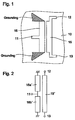
- FIG. 1 illustrates the configuration of a balance-unbalance converter according to a first embodiment of the present invention
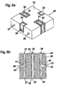
- FIG. 2 is an equivalent circuit diagram of the balance-unbalance converter
- FIG. 3A is a perspective view showing the appearance of a balance-unbalance converter according to a second embodiment of the present invention.
- FIG. 3B is a cross section of the balance-unbalance converter
- FIG. 4 illustrates the configuration of a balance-unbalance converter according to a third embodiment of the present invention
- FIG. 5 is an equivalent circuit diagram of the balance-unbalance converter
- FIG. 6A is a perspective view showing the appearance of a balance-unbalance converter according to a fourth embodiment of the present invention.
- FIG. 6B is a cross section of the balance-unbalance converter
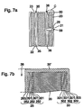
- FIG. 7A is a cross section of a balance-unbalance converter according to a fifth embodiment of the present invention.
- FIG. 7B is a fragmentary cross section of the balance-unbalance converter
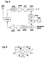
- FIG. 8 is a block diagram showing the configuration of a communication device according to a sixth embodiment of the present invention.
- FIG. 9 illustrates the configuration of a conventional balance-unbalance converter.
- FIG. 1 is a plan view of the balance-unbalance converter.
- Strip line electrodes 15 and 16 are arranged, adjacently in parallel to each other on the upper face of a dielectric substrate 10.
- An earth electrode is formed so as to extend substantially on the whole of the under face of the dielectric substrate 10.
- the dielectric substrate 10, the strip line electrodes 15 and 16, and the earth electrode constitute microstrip lines, respectively.
- a terminal electrode 11 is led out from the center of the strip line electrode 16, and terminal electrodes 12 and 13 are led out from both of the ends of the strip line electrode 15.
- Both of the ends of the strip line electrode 16 are patterned so as to be connected to earth electrodes, respectively, provided on the upper face of the dielectric substrate 10.
- FIG. 2 is an equivalent circuit diagram of the balance-unbalance converter shown in FIG. 1.
- a microstrip line 15' corresponds to the microstrip line electrode 15 shown in FIG. 1
- microstrip lines 16a' and 16b' correspond to the microstrip line electrode 16 in FIG. 1, respectively.
- the microstrip line 15' having the open opposite ends, and the microstrip lines 16a' and 16b' each having the grounded end are arranged adjacently in parallel to each other, as described above. Therefore, both of the microstrip lines 15' and 16a' and 16b' are coupled to each other via an electromagnetic field.
- the ground ends of the microstrip lines 16a' and 16b' have a ground potential, and the potential of the terminal electrode 11 is varied correspondingly to an unbalance input voltage with respect to the ground potential.
- output voltages having a phase difference of 180° are generated at both of the open ends of the microstrip line 15'.
- the terminal electrode 11 acts as an unbalanced input port
- the terminal electrodes 12 and 13 act as balanced output ports.
- the terminal electrodes 12 and 13 may be employed as balanced input ports, and the terminal electrode 11 may be used as an unbalanced output port, due to the reversibility of the circuit.
- FIG. 3A is a perspective view showing the appearance of the balance-unbalance converter.
- FIG. 3B is a cross section taken along the plane passing through two inner conductor formation holes 35 and 36 shown in FIG. 3A.
- Terminal electrodes 21, 22, and 23 are connected to signal input-output electrodes formed on the circuit substrate.
- An earth electrode on the circuit substrate is connected to an outer conductor 30.
- a dielectric block 20 has a substantially rectangular parallelepiped shape as a whole, and is provided with three inner conductor formation holes 35, 36, and 38.
- the two inner conductor formation holes 35 and 36 of these holes are formed in parallel to each other.
- the inner conductor formation hole 38 is formed orthogonally to the inner conductor formation hole 36.
- Inner conductors 25, 26, and 28 are formed on the inner walls of the inner conductor formation holes 35, 36, and 38, respectively.
- terminal electrodes 22 and 23 are formed at both of the ends of the inner conductor formation hole 35 so as to be connected to the inner conductor 25 and separated from the outer conductor 30.
- a terminal electrode 21 is formed at the opening of the inner conductor formation hole 38 so as to be connected to the inner conductor 28 and separated from the outer conductor 30.
- both of the ends of the inner conductor 26 formed on the inner wall of the inner conductor formation hole 36 are connected to the outer conductor 30.
- FIG. 4 is a plane view of the balance-unbalance converter.
- Strip line electrodes 16 and 17 are arranged adjacently to and on both sides of a strip line electrode 15, on the upper face of a dielectric substrate 10.
- An earth electrode is formed substantially on the whole of the under face of the dielectric substrate 10.
- the dielectric substrate 10, the strip line electrodes 15, 16, and 17, and the earth electrode constitute microstrip lines, respectively.
- Terminal electrodes 11 and 14 are led out from the centers of the strip line electrodes 16 and 17, respectively.
- Terminal electrodes 12 and 13 are led out from both of the ends of the strip line electrode 15, respectively. Both of the ends of each strip line 16 and 17 are patterned so as to be connected to an earth electrode provided on the upper face of the dielectric substrate 10.
- FIG. 5 is an equivalent circuit diagram of the balance-unbalance converter of FIG. 4.
- a microstrip line 15' corresponds to the strip line electrode 15 shown in FIG. 1.
- Microstrip lines 16a' and 16b' correspond to the microstrip line electrode 16 shown in FIG. 1.
- Microstrip lines 17a' and 17b' correspond to the microstrip line electrode 17 shown in FIG. 1.
- the microstrip line 15'having both of the ends opened and the microstrip line 16a' and 16b' having both of the ends grounded are arranged adjacently to and in parallel to each other to be coupled via an electromagnetic field.
- the microstrip line 15' and the microstrip lines 17a' and 17b' are coupled to each other via an electromagnetic field.
- the total electrical length of the microstrip lines 16a' and 16b' is different from that of the microstrip lines 17a' and 17b'. Furthermore, the electrical length of the microstrip line 15'is in the range between the total electrical length of the lines 16a' and 16b' and that of the lines 17a' and 17b'.
- the microstrip line 15' and the microstrip lines 16a' and 16b' act as a balance-unbalance converter in a first frequency band, and simultaneously, the microstrip line 15' and the microstrip lines 17a' and 17b' act as a balance-unbalance converter in a second frequency band.
- the balance-unbalance converter of this embodiment can be used as a multiplexer having a function of inputting signals in the first and second frequency bands via the terminal electrodes 11 and 14 as unbalanced input ports, and outputting the multiplexed signals from the terminal electrodes 12 and 13 as balanced output ports.
- the balance-unbalance converter of this embodiment can be employed as a demultiplexer having a function of demultiplexing an input signal into signals in the first and second frequency bands by use of the terminal electrodes 12 and 13 as balanced input ports and the terminal electrodes 11 and 14 as unbalanced output ports.
- the difference between the electrical length of the microstrip line 15' and the overall electrical length of the microstrip lines 16a' and 16b', and that between the electrical length of the microstrip line 15' and the overall electrical length of the microstrip lines 17a'and 17b' are small. Accordingly, good multiplexing and demultiplexing characteristics in the above-mentioned first and second frequency bands can be obtained.
- FIGS. 6A and 6B the configuration of a balance-unbalance converter having a multiplexing or demultiplexing function according to a fourth embodiment of the present invention will be described with reference to FIGS. 6A and 6B.
- FIG. 6A is a perspective view showing the appearance of the balance-unbalance converter.
- FIG. 6B is a cross section thereof taken along the plane passing through two inner conductor formation holes shown in FIG. 6A.
- the upper face as viewed in FIG. 6A of the balance-unbalance converter, when the converter is surface-mounted, is used as a mounting surface opposed to a circuit substrate.
- Terminal electrodes 21, 22, 23, and 24 are connected to signal input-output terminals provided on the circuit substrate, respectively.
- An outer conductor 30 is connected to an earth electrode on the circuit substrate.
- a dielectric block 20 has a substantially rectangular parallelepiped shape as a whole, and is provided with three inner conductor formation holes 35, 36, and 37, and two slits 39 and 40.
- the three inner conductor formation holes 35, 36, and 37 are formed in parallel to each other.
- the slits 39 and 40 are formed orthogonally to the inner conductor formation holes 36 and 37, respectively.
- Inner conductors 25, 26, and 27 are formed on the inner walls of the inner conductor formation holes 35, 36, and 37, and inner conductors 41 and 42 are formed on the inner walls of slits 39 and 40, respectively.
- terminal electrodes 22 and 23 are formed at both of the ends of the inner conductor formation hole 35 so as to be connected to the inner conductor 25 and separated from an outer conductor 30.
- Terminal electrodes 21 and 24 are formed at the openings of the slits 39 and 40 so as to be connected to the inner conductor 41 and 42 and separated from the outer conductor 30.
- Both of the ends of the inner conductors 26 and 27 formed on the inner walls of the inner conductor formation holes 36 and 37 are connected to the outer conductor 30.
- a multiplexer or demultiplexer which contains the terminal electrodes 21 and 24 as unbalanced ports, and the terminal electrodes 22 and 23 as balanced ports, equivalently similarly to the configuration of FIG. 5.
- each of the conductor films in the main parts comprises a thin film lamination electrode.
- FIG. 7A is a cross section of the converter taken along the same plane thereof as that of the second embodiment shown in FIG. 3B.
- FIG. 7B is an enlarged view of part C shown in FIG. 7A.
- the thickness of a dielectric block 20 is considerably shortened as compared with the thickness of the respective thin film conductor layers or the like.
- thin film conductor layers 261 and 301, thin film dielectric layers 262 and 302, and outermost conductor layers 263 and 303 are shown.
- the thin film conductor layers 261 and 301 and the thin film dielectric layers 262 and 302 are alternately laminated to each other.
- the inner conductor 26 and the outer conductor 30 each having the thin film lamination electrode structure are formed.
- Conductor layers 263 and 303 having a large thickness are provided as the outermost layers, respectively, and thereby, the surfaces of the thin film lamination electrodes become fast.
- An outer conductor 30' comprising a single layer electrode having a thickness at least three times the skin depth at an operating frequency is formed on a short-circuiting face of the dielectric block 20 so as to connect the inner conductor 26 and the outer conductor 30 each having the thin film lamination electrode structure, and also, connect the respective thin film conductor layers to each other.
- the part of the inner conductor 25 has a thin film lamination electrode structure.
- a transmission-reception antenna ANT, a duplexer DPX, band-pass filters BPFa, BPFb, and BPFc, amplifier circuits AMPa and AMPb, balance-unbalance converters BUa and BUb, mixers MIXa and MIXb, an oscillator OSC, and a frequency divider (synthesizer) DIV constitutes the communication device.
- the mixer MIXa modulates a frequency signal output from the frequency divider DIV, with a modulation signal.
- the band-pass filter BPFa transmits only a signal within a transmission frequency band.
- the amplifier circuit AMPa power-amplifies the signal, and transmits the signal from the antenna ANT via the duplexer DPX.
- the band-pass filter BPFb transmits only a signal output from the duplexer DPX and within a reception frequency band.
- the amplifier circuit AMPb amplifies the signal.
- the mixer MIXb mixes a frequency signal output from the band-pass filter BPFc and the reception signal to output an intermediate frequency signal IF.
- the amplifier circuit AMPa is a balanced input type amplifier circuit
- the amplifier circuit AMPb is an unbalanced output type amplifier circuit.
- the balance-unbalance converter BUa converts an unbalanced output signal from the band-pass filter BPFa to a balanced signal, and feeds the signal to the amplifier circuit AMPa.
- the balance-unbalance converter BUb converts an unbalanced output signal from the amplifier circuit AMPb to a balanced signal, and feeds the signal to the mixer MIXb.
- the transmission lines each comprise the microstrip lines.
- the transmission lines may comprise strip lines each produced by forming dielectric layers and earth electrodes on both of the upper and under faces of a strip line electrode, respectively.
- the coaxial transmission lines are formed by use of the single dielectric blocks, respectively.
- Two dielectric sheets each having a groove formed thereon may be used. Inner conductors are formed on the inner walls of the grooves, and outer conductors are formed on the back faces of the dielectric sheets, respectively. Then, the two dielectric sheets are bonded to each other, so that the balance-unbalance converter including the formed coaxial structure transmission lines is produced.
- the interval between the balanced ports can be set to be relatively wide, and the connection of the balanced ports (parallel input-output terminals) to transmission lines can be easily performed, due to the configuration. Therefore, no unnecessary coupling between the parallel terminals occurs, and an excellent balance characteristic can be obtained.
- the balance-unbalance converting circuit can be used as a three port type provided with one balanced port and two unbalanced ports, and having a function of multiplexing or demultiplexing a signal. Furthermore, the balance-unbalance converting circuit can be reduced in size as a whole.
- the electrical length of the above-described first transmission line may be set to be in the range between the electrical lengths of the first and second transmission lines. Accordingly, a balance-unbalance converter made up of the first and second transmission lines, and a balance-unbalance converting circuit made up of the first and third transmission lines exhibit good balance-unbalance conversion characteristics with respect to two frequency bands. That is, for the two frequency bands, good multiplexing or demultiplexing characteristics can be attained.
- the transmission lines may comprise microstrip or strip lines produced by forming conductor films on a dielectric substrate, respectively.
- the balance-unbalance converter including the dielectric substrate can be simply formed.
- the balance-unbalance converter can be easily connected to other high frequency circuits.
- the transmission lines may comprise the dielectric coaxial lines produced by forming conductor films in a dielectric block, respectively.
- the conductor films is a thin film lamination electrode having an area in which plural thin film conductor layers and plural thin film dielectric layers, each having a thickness smaller than the skin depth at an operating frequency are alternately laminated.
- the effective sectional area of the thin film lamination electrode is increased.
- the conductor loss, caused by the skin effect, is reduced.
- the balance-unbalance converter having a low loss can be obtained.
- a communication device reduced in size, having a high efficiency can be obtained.
Landscapes
- Coils Or Transformers For Communication (AREA)
- Waveguides (AREA)
- Control Of Motors That Do Not Use Commutators (AREA)
Abstract
Description
respectively.
Claims (7)
- A balance-unbalance converting circuit comprising a first transmission line (15, 15'; 25) having both of the ends opened, and a second transmission line (16, 16a', 16b'; 26) having both of the ends grounded, arranged substantially in parallel to the first transmission line (15, 15'; 25), and having an electrical length substantially equal to the electrical length of the first transmission line (15, 15'; 25), said first transmission line (15, 15'; 25) having balanced ports (12, 13; 22, 23) connected to both of the ends thereof, said second transmission line (16, 16a', 16b'; 26) having an unbalanced port (11; 21) connected substantially to the center thereof.
- A balance-unbalance converting circuit according to claim 1, wherein a third transmission (17, 17a', 17b'; 27) line having both of the ends thereof grounded is provided substantially in parallel to the first transmission line (15, 15'; 25), the electrical length of the third transmission line (17, 17a', 17b'; 27) is substantially equal to the electrical length of the first transmission line (15, 15'; 25) and is different from the electrical length of the second transmission line (16, 16a', 16b';26), and the third transmission line (17, 17a', 17b'; 27) has an unbalanced port (14; 24) connected substantially to the center thereof.
- A balance-unbalance converting circuit according to claim 2, wherein the electrical length of the first transmission line (15, 15'; 25) is in the range between the electrical lengths of the second (16, 16a', 16b'; 26) and third transmission lines (17, 17a', 17b'; 27).
- A balance-unbalance converter including the transmission lines (15, 15', 16, 16a', 16b'; 17, 17a', 17b'; 25, 26, 27) defined in claim 1, 2, or 3 each comprising a microstrip line or strip line (15, 15', 16, 16a', 16b', 17, 17a', 17b') produced by forming a conductor film on a dielectric substrate (10).
- A balance-unbalance converter including the transmission lines (15, 15', 16, 16a', 16b'; 17, 17a', 17b'; 25, 26, 27) defined in claim 1, 2, or 3 each comprising a dielectric coaxial transmission line (25, 26, 27) produced by forming a conductor film in a dielectric block (20).
- A balance-unbalance converter according to claim 4 or 5, wherein at least a part of the conductor films comprise a thin film lamination electrode having an area in which plural thin film conductor layers (261, 301) and plural thin film dielectric layers (262, 302), each having a thickness smaller than the skin depth at an operating frequency are alternately laminated.
- A communication device including a balance-unbalance converter defined in claim 4, 5, or 6.
Applications Claiming Priority (4)
| Application Number | Priority Date | Filing Date | Title |
|---|---|---|---|
| JP32572699 | 1999-11-16 | ||
| JP32572699 | 1999-11-16 | ||
| JP2000259654 | 2000-08-29 | ||
| JP2000259654A JP2001211010A (en) | 1999-11-16 | 2000-08-29 | Balance/unbalance conversion circuit, balance/unbalance converter and communications equipment |
Publications (2)
| Publication Number | Publication Date |
|---|---|
| EP1102345A2 true EP1102345A2 (en) | 2001-05-23 |
| EP1102345A3 EP1102345A3 (en) | 2002-03-27 |
Family
ID=26571928
Family Applications (1)
| Application Number | Title | Priority Date | Filing Date |
|---|---|---|---|
| EP00123559A Withdrawn EP1102345A3 (en) | 1999-11-16 | 2000-10-27 | Balance-unbalance converting circuit, balance-unbalance converter, and communication device including the same |
Country Status (3)
| Country | Link |
|---|---|
| US (1) | US6448864B1 (en) |
| EP (1) | EP1102345A3 (en) |
| JP (1) | JP2001211010A (en) |
Cited By (1)
| Publication number | Priority date | Publication date | Assignee | Title |
|---|---|---|---|---|
| CN100466373C (en) * | 2004-02-06 | 2009-03-04 | 株式会社村田制作所 | Balanced distributor |
Families Citing this family (3)
| Publication number | Priority date | Publication date | Assignee | Title |
|---|---|---|---|---|
| JP3866231B2 (en) * | 2003-09-04 | 2007-01-10 | Tdk株式会社 | Multilayer bandpass filter |
| DE102004022185A1 (en) * | 2004-05-05 | 2005-12-01 | Rohde & Schwarz Gmbh & Co. Kg | Broadband balun transformer |
| KR100715861B1 (en) | 2006-02-17 | 2007-05-11 | 삼성전자주식회사 | Balloon |
Family Cites Families (11)
| Publication number | Priority date | Publication date | Assignee | Title |
|---|---|---|---|---|
| JPS607407B2 (en) * | 1977-08-20 | 1985-02-25 | 日立電線株式会社 | Balanced-unbalanced converter |
| JPS60148233A (en) * | 1984-01-13 | 1985-08-05 | Matsushita Electric Ind Co Ltd | Mixer circuit |
| US5229782A (en) * | 1991-07-19 | 1993-07-20 | Conifer Corporation | Stacked dual dipole MMDS feed |
| CN1122327C (en) * | 1993-08-27 | 2003-09-24 | 株式会社村田制作所 | Thin-film multilayer electrode of high frequency electromagnetic field coupling |
| JP2773617B2 (en) * | 1993-12-17 | 1998-07-09 | 株式会社村田製作所 | Balun Trance |
| US5777527A (en) * | 1996-10-31 | 1998-07-07 | Motorola, Inc. | Method and apparatus for coupling a differential signal to an unbalanced port |
| US5880646A (en) * | 1997-05-07 | 1999-03-09 | Motorola, Inc. | Compact balun network of doubled-back sections |
| JPH11214943A (en) * | 1998-01-26 | 1999-08-06 | Murata Mfg Co Ltd | Balloon transformer |
| US6294965B1 (en) * | 1999-03-11 | 2001-09-25 | Anaren Microwave, Inc. | Stripline balun |
| JP3528044B2 (en) * | 1999-04-06 | 2004-05-17 | 株式会社村田製作所 | Dielectric filter, dielectric duplexer and communication device |
| JP2001036310A (en) * | 1999-07-23 | 2001-02-09 | Nec Corp | 180-degree phase shifter |
-
2000
- 2000-08-29 JP JP2000259654A patent/JP2001211010A/en active Pending
- 2000-10-27 EP EP00123559A patent/EP1102345A3/en not_active Withdrawn
- 2000-11-16 US US09/714,763 patent/US6448864B1/en not_active Expired - Lifetime
Cited By (1)
| Publication number | Priority date | Publication date | Assignee | Title |
|---|---|---|---|---|
| CN100466373C (en) * | 2004-02-06 | 2009-03-04 | 株式会社村田制作所 | Balanced distributor |
Also Published As
| Publication number | Publication date |
|---|---|
| JP2001211010A (en) | 2001-08-03 |
| EP1102345A3 (en) | 2002-03-27 |
| US6448864B1 (en) | 2002-09-10 |
Similar Documents
| Publication | Publication Date | Title |
|---|---|---|
| JP3642276B2 (en) | Antenna device and communication device | |
| US6801101B2 (en) | Dielectric filter, dielectric duplexer, and communication apparatus | |
| EP0986124B1 (en) | Dielectric filter, composite dielectric filter, antenna duplexer, and comunication apparatus | |
| KR100353593B1 (en) | Dielectric filter, duplexer and communication apparatus | |
| US6549093B2 (en) | Dielectric filter, duplexer, and communication apparatus incorporating the same | |
| JP3480368B2 (en) | Dielectric filter, dielectric duplexer and communication device | |
| US6448864B1 (en) | Balanced-unbalanced converting circuit, balanced-unbalanced converter, and communication device including the same | |
| KR100352573B1 (en) | Dielectric Filter, Dielectric Duplexer, and Communication Apparatus | |
| JP2003087014A (en) | Nonreciprocal circuit element and communication apparatus | |
| KR100411203B1 (en) | Dielectric Filter, Dielectric Duplexer and Communication Apparatus incorporating the Same | |
| JP3788402B2 (en) | Dielectric filter, dielectric duplexer, and communication device | |
| KR100519014B1 (en) | Dielectric filter, dielectric duplexer and communication apparatus |
Legal Events
| Date | Code | Title | Description |
|---|---|---|---|
| PUAI | Public reference made under article 153(3) epc to a published international application that has entered the european phase |
Free format text: ORIGINAL CODE: 0009012 |
|
| 17P | Request for examination filed |
Effective date: 20001027 |
|
| AK | Designated contracting states |
Kind code of ref document: A2 Designated state(s): DE FR GB Kind code of ref document: A2 Designated state(s): AT BE CH CY DE DK ES FI FR GB GR IE IT LI LU MC NL PT SE |
|
| AX | Request for extension of the european patent |
Free format text: AL;LT;LV;MK;RO;SI |
|
| PUAL | Search report despatched |
Free format text: ORIGINAL CODE: 0009013 |
|
| AK | Designated contracting states |
Kind code of ref document: A3 Designated state(s): AT BE CH CY DE DK ES FI FR GB GR IE IT LI LU MC NL PT SE |
|
| AX | Request for extension of the european patent |
Free format text: AL;LT;LV;MK;RO;SI |
|
| AKX | Designation fees paid |
Free format text: DE FR GB |
|
| STAA | Information on the status of an ep patent application or granted ep patent |
Free format text: STATUS: THE APPLICATION HAS BEEN WITHDRAWN |
|
| 18W | Application withdrawn |
Effective date: 20051117 |