EP1102344A2 - Dielectric resonator, dielectric filter, dielectric duplexer, and communication device - Google Patents
Dielectric resonator, dielectric filter, dielectric duplexer, and communication device Download PDFInfo
- Publication number
- EP1102344A2 EP1102344A2 EP00122900A EP00122900A EP1102344A2 EP 1102344 A2 EP1102344 A2 EP 1102344A2 EP 00122900 A EP00122900 A EP 00122900A EP 00122900 A EP00122900 A EP 00122900A EP 1102344 A2 EP1102344 A2 EP 1102344A2
- Authority
- EP
- European Patent Office
- Prior art keywords
- dielectric
- thin
- film
- face
- outer conductor
- Prior art date
- Legal status (The legal status is an assumption and is not a legal conclusion. Google has not performed a legal analysis and makes no representation as to the accuracy of the status listed.)
- Granted
Links
- 238000004891 communication Methods 0.000 title claims abstract description 11
- 239000010409 thin film Substances 0.000 claims abstract description 112
- 239000004020 conductor Substances 0.000 claims abstract description 109
- 239000010410 layer Substances 0.000 claims abstract description 83
- 239000002356 single layer Substances 0.000 claims abstract description 10
- 230000008878 coupling Effects 0.000 description 9
- 238000010168 coupling process Methods 0.000 description 9
- 238000005859 coupling reaction Methods 0.000 description 9
- 239000010408 film Substances 0.000 description 7
- 230000005540 biological transmission Effects 0.000 description 6
- 238000010586 diagram Methods 0.000 description 6
- 238000009826 distribution Methods 0.000 description 5
- 238000006073 displacement reaction Methods 0.000 description 4
- 230000005684 electric field Effects 0.000 description 4
- 239000000758 substrate Substances 0.000 description 4
- 238000003780 insertion Methods 0.000 description 3
- 230000037431 insertion Effects 0.000 description 3
- UUDAMDVQRQNNHZ-UHFFFAOYSA-N (S)-AMPA Chemical compound CC=1ONC(=O)C=1CC(N)C(O)=O UUDAMDVQRQNNHZ-UHFFFAOYSA-N 0.000 description 2
- 239000003989 dielectric material Substances 0.000 description 2
- 238000000034 method Methods 0.000 description 2
- 239000007787 solid Substances 0.000 description 2
- 238000005299 abrasion Methods 0.000 description 1
- 238000005520 cutting process Methods 0.000 description 1
- 230000001419 dependent effect Effects 0.000 description 1
- 238000000151 deposition Methods 0.000 description 1
- 230000002500 effect on skin Effects 0.000 description 1
- 230000005672 electromagnetic field Effects 0.000 description 1
- 238000005530 etching Methods 0.000 description 1
- 238000007733 ion plating Methods 0.000 description 1
- 239000000463 material Substances 0.000 description 1
- 230000001902 propagating effect Effects 0.000 description 1
- 230000005855 radiation Effects 0.000 description 1
- 238000004544 sputter deposition Methods 0.000 description 1
- 239000000126 substance Substances 0.000 description 1
- 238000007738 vacuum evaporation Methods 0.000 description 1
Images



Classifications
-
- H—ELECTRICITY
- H01—ELECTRIC ELEMENTS
- H01P—WAVEGUIDES; RESONATORS, LINES, OR OTHER DEVICES OF THE WAVEGUIDE TYPE
- H01P1/00—Auxiliary devices
- H01P1/20—Frequency-selective devices, e.g. filters
- H01P1/201—Filters for transverse electromagnetic waves
- H01P1/205—Comb or interdigital filters; Cascaded coaxial cavities
- H01P1/2056—Comb filters or interdigital filters with metallised resonator holes in a dielectric block
-
- H—ELECTRICITY
- H01—ELECTRIC ELEMENTS
- H01P—WAVEGUIDES; RESONATORS, LINES, OR OTHER DEVICES OF THE WAVEGUIDE TYPE
- H01P7/00—Resonators of the waveguide type
- H01P7/04—Coaxial resonators
-
- H—ELECTRICITY
- H01—ELECTRIC ELEMENTS
- H01P—WAVEGUIDES; RESONATORS, LINES, OR OTHER DEVICES OF THE WAVEGUIDE TYPE
- H01P1/00—Auxiliary devices
- H01P1/20—Frequency-selective devices, e.g. filters
- H01P1/207—Hollow waveguide filters
- H01P1/208—Cascaded cavities; Cascaded resonators inside a hollow waveguide structure
- H01P1/2084—Cascaded cavities; Cascaded resonators inside a hollow waveguide structure with dielectric resonators
-
- H—ELECTRICITY
- H01—ELECTRIC ELEMENTS
- H01P—WAVEGUIDES; RESONATORS, LINES, OR OTHER DEVICES OF THE WAVEGUIDE TYPE
- H01P1/00—Auxiliary devices
- H01P1/20—Frequency-selective devices, e.g. filters
- H01P1/213—Frequency-selective devices, e.g. filters combining or separating two or more different frequencies
- H01P1/2136—Frequency-selective devices, e.g. filters combining or separating two or more different frequencies using comb or interdigital filters; using cascaded coaxial cavities
-
- H—ELECTRICITY
- H01—ELECTRIC ELEMENTS
- H01P—WAVEGUIDES; RESONATORS, LINES, OR OTHER DEVICES OF THE WAVEGUIDE TYPE
- H01P7/00—Resonators of the waveguide type
- H01P7/10—Dielectric resonators
Definitions
- the present invention relates to a dielectric resonator, a dielectric filter, and a dielectric duplexer, which include a dielectric block and conductive layers serving as electrodes formed on the inner and outer surfaces of the dielectric block, and also to a communication device using at least one of the dielectric resonator, the dielectric filter, and the dielectric duplexer.
- a typical dielectric resonator for use in the microwave band is formed using a rectangular or cylindrical dielectric block having a coaxial through-hole wherein an inner conductor is formed on the inner surface of the through-hole and an outer conductor is formed on the outer surface of the dielectric block. It is also known in the art to construct a dielectric filter or a dielectric duplexer having a plurality of resonator stages by forming a plurality of through-holes in a rectangular dielectric block and forming inner conductors on the inner surfaces of the respective through-holes thereby forming a plurality of dielectric resonators in the single dielectric block.
- Devices such as the dielectric resonator and the dielectric filter constructed by forming conductive films serving as electrodes on the inner and outer surfaces of a dielectric block have the advantages that the total size is small and high unloaded Q (Qo) is obtained.
- the loss of dielectric resonators includes conductor losses of conductive films such as an inner conductor and an outer conductor, a dielectric loss of a dielectric material, and a radiation loss radiated to the outside. Of these losses, the conductor loss is dominant. Therefore, the key point for reducing the loss of dielectric resonators is to reduce the conductive loss.
- the conductive films will have a reduced current density, and thus the conductive loss will be reduced.
- this technique cannot meet the requirement of reducing the size.
- the present invention provides a dielectric resonator comprising a dielectric block, an inner conductor formed on the inner surface of a through-hole extending from one end face to the opposite end face of the dielectric block, and an outer conductor formed on the outer surface of the dielectric block, wherein at least a part of at least one of the inner conductor and the outer conductor has a thin-film multilayer electrode structure formed by alternately disposing thin-film conductive layers with a thickness smaller than the skin depth at the operating frequency and thin-film dielectric layers with a particular dielectric constant, thereby allowing currents to be passed substantially equally through the respective thin-film conductive layers of the thin-film multilayer electrodes and thus achieving an increase in the effective area (effective cross section) of current paths and a reduction in the conductor loss.
- a dielectric resonator with a low loss is achieved.
- the present invention also provides a dielectric filter comprising the dielectric block described above and external terminals serving as high frequency signal input/output terminals.
- the dielectric block preferably includes a plurality of through-holes, and closest parts of the inner conductors formed on the inner surfaces of the through-holes preferable have the thin-film multilayer electrode structure.
- the thin-film multilayer electrodes are provided at locations where the electric field is concentrated in the odd mode of the coupling modes of the two resonators, thereby efficiently improving the insertion loss of the dielectric filter.
- the present invention also provides a dielectric duplexer comprising the dielectric block described above, an external terminal for connection with an antenna, an external terminal for connection with a receiving circuit, and an external terminal for connection with a transmitting circuit, wherein the external terminals are disposed on the outer surface of the dielectric block.
- This dielectric duplexer using the single dielectric block may be employed, for example, as an antenna duplexer having a transmission filter and a reception filter.
- the present invention also provides a communication device including the above-described dielectric filter serving, for example, as a transmission/reception signal band-pass filter or including the above-described dielectric duplexer serving as an antenna duplexer.
- a communication device having a small size and having a high power efficiency can be realized.
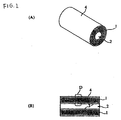
- Fig. 1A is a perspective view illustrating the appearance of the dielectric resonator
- Fig. 1B is a cross-sectional view thereof taken along the central axis.
- reference numeral 1 denotes a cylindrical-shaped dielectric block having a through-hole 2 extending along the central axis from one end face to the opposite end face.
- An inner conductor 3 is formed on the inner surface of the through-hole 2
- an outer conductor 4 is formed on the outer surface of the dielectric block 1.
- the inner conductor 3 and the outer conductor 4 are both formed so as to have a thin-film multilayer electrode structure consisting of a plurality of thin-film conductive layers and thin-film dielectric layers which are alternately disposed one on another.
- Fig. 2 is a cross-sectional view of a part denoted by D in Fig. 1B. Note that in Fig. 2 the thickness of the dielectric block 1 is much reduced relative to the thicknesses of the thin-film conductive layers.
- solid arrows represent high frequency currents and broken arrows represent displacement currents.
- Reference numerals 31 and 41 denote thin-film conductive layers with a thickness equal to or smaller than the skin depth at the operating frequency.
- Reference numerals 33 and 43 denote outermost conductive layers.
- the inner conductor 3 and the outer conductor 4 with the thin-film multilayer electrode structure are produced by alternately disposing thin-film conductive layers and thin-film dielectric layers.
- the outermost conductive layers are formed so as to have a large thickness thereby achieving ruggedness of the surfaces of the thin-film multilayer electrodes. This allows the multilayer structure made up of the thin-film conductive layers and the thin-film dielectric layers to be maintained without being deformed when a pin electrode is inserted into the though-hole 2 so as to achieve electrical connection with the inner conductor 3, or when the outer electrode 4 of the dielectric resonator is soldered to a ground electrode on a mounting substrate.
- the numbers of thin-film conductive layers and thin-film dielectric layers may be 2, the thickness of each thin-film conductive layer may be 1823 nm, the thickness of each dielectric layer may be 113 nm, and the thickness of each outermost conductive layer may be 6000 nm, although specific values may be varied depending upon the operating frequency.
- a high frequency signal is applied between the outermost conductive layers 33 and 43, a high frequency electric field is applied across the dielectric block 1 as shown in Fig. 2, and resonance occurs.
- the high-frequency electric power applied, via thin-film dielectric layers at lower positions, to the respective thin-film conductive layers 31 and 41 is partially transmitted to thin-film conductive layers located at upper positions, and the energy of the high-frequency signal is partially reflected back to the thin-film conductive layers at the lower positions via the thin-film dielectric layers at the lower positions.
- each thin-film dielectric layer located between adjacent two thin-film conductive layers the reflected and transmitted waves resonate, and high-frequency currents flow in the upper surface region and the lower surface region of each thin-film conductive layer such that they flow along the surfaces in parallel but in opposite directions. Because the film thicknesses of the thin-film conductive layers 31 and 41 are smaller than the skin depth, the two high-frequency currents flowing in parallel in the opposite directions interfere with each other via the thin-film dielectric layer. As a result, almost all currents are cancelled.
- the dielectric resonator acts as a half-wave coaxial resonator which is open-circuited at both ends, and thus the displacement currents become maximum at both ends, in the longitudinal direction, of the inner conductor 3 and become minimum at the center thereof.
- the thicknesses of the respective thin-film dielectric layers 32 and 42 are selected so that the phase velocities of TEM waves propagating through the dielectric block 1 and the thin-film dielectric layers 32 and 42 become substantially equal. Therefore, the high-frequency currents flowing in a distributed fashion through the thin-film conductive layers 31 and 41 become equal in phase. This results in an increase in the effective skin depth.
- the increased effective skin depth is obtained by distributing the currents among the thin-film conductive layers 31 and 41 such that the distributed currents flow with the same phase.
- the effective areas (effective cross sections) of the current paths are increased and thus the conductor losses are reduced.
- a dielectric resonator with a low loss is obtained.
- both inner and outer conductors are formed so as to have the thin-film multilayer electrode structure, only either the outer conductor or the inner conductor may have the thin-film multilayer electrode structure.
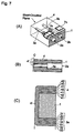
- Fig. 3A is a perspective view illustrating the appearance of the dielectric resonator
- Fig. 3B is a cross-sectional view thereof taken along the central axis
- Fig. 3C is an enlarged view of a part denoted by C in Fig. 3B.
- one end face, on a front side in Fig. 3A, of a dielectric block 1 is formed so as to act as an open-circuited end, and the opposite end face is formed so as to act as a short-circuited end.
- An inner conductor 3 and an outer conductor 4 are formed on the inner surface of a through-hole 2 and the outer surface of the dielectric block 1, respectively, in a similar manner to the first embodiment.
- a part denoted by D in Fig. 3B has an electrode structure similar to that shown in Fig. 2, although the distributions of currents and displacement currents are different.
- An outer conductor 4' in the form of a single-layer electrode is disposed on the short-circuited end face of the dielectric block 1 such that an end of the inner conductor 3 with the thin-film multilayer electrode structure and an end of the outer conductor 4 with the thin-film multilayer electrode structure are electrically connected to each other via the outer conductor 4'.
- the outer conductor 4' connects together the thin-film conductive layers 31 and the outermost conductor layer 33 of the inner conductor 3 and also connects together the thin-film conductive layers 41 and the outermost conductive layer 43 of the outer conductor 4.
- the respective thin-film conductive layers have the common zero potential, and high-frequency currents flowing through the respective thin-film conductive layers have the same phase.
- the effective skin depth is increased.
- the conductor loss of the outer conductor 4' can be minimized by forming the outer conductor 4' so as to have a thickness equal to or greater than the skin depth at the operating frequency.
- the outer conductor 4' on the short-circuited end face is in the form of a single-layer electrode, it is possible to adjust the resonance frequency of the dielectric resonator simply by cutting a part of the outer conductor 4' by a particular amount.
- Fig. 4 is a perspective view illustrating the appearance of the dielectric filter. Note that the dielectric filter is drawn such that the plane to be in contact with a mounting substrate is on the top side of Fig. 4.
- reference numeral 1 denotes a rectangular dielectric block.
- through-holes 2a and 2b are formed between two opposite end faces such that the axes thereof become parallel to each other.
- the through-holes 2a and 2b have a stepped structure in terms of the hole diameter along the axis thereof. That is, the through-hole 2a and 2b includes a small-diameter part with a small hole diameter formed in the center and large-diameter parts with a large hole diameter formed on both end sides.
- Inner conductors 3a and 3b are formed on the inner surfaces of the respective through-holes 2a and 2b.
- an outer conductor 4 is formed on four side faces other than the two end faces between which the through-holes 2a and 2b are formed.
- signal input/output terminals 7a and 7b for inputting/outputting a high frequency signal are formed on the outer surface of the dielectric block 1 such that they are electrically isolated from the outer conductor 4.
- Fig. 5A is a view of the dielectric filter shown in Fig. 4, seen from the side of one end face in which open ends of the through-holes 2a and 2b are formed.
- Fig. 5B is an enlarged view of a part denoted by B in Fig. 5A.
- the outer conductor 4 has a thin-film multilayer electrode structure consisting of an outermost conductive layer 43 and a multilayer region including thin-film conductive layers 41 and thin-film dielectric layers 42.
- the thin-film conductive layers 41 and the thin-film dielectric layers 42 extend continuously along a ridge from one side face of the dielectric block 1 to another adjacent side face.
- the inner conductors 3a and 3b also have a thin-film multilayer electrode structure similar to that shown in Fig. 2.
- two half-wave resonators coupled to each other are formed in the single dielectric block.
- the signal input/output terminals 7a and 7b are formed by first forming the thin-film multilayer electrode over the entire areas of the four side faces of the dielectric block 1 and then selectively etching the thin-film multilayer electrode so as to form portions isolated from the other portion of the outer conductor 4.
- the signal input/output terminals 7a and 7b creates electrostatic capacity with one open end of each inner conductor 3a and 3b, and thus the signal input/output terminals 7a and 7b are capacitively coupled with the respective resonators.
- the signal input/output terminals 7a and 7b may be formed so as to have a thin-film multilayer electrode structure, like the outer conductor 4, or may be formed so as to have a single-layer electrode structure because the signal input/output terminals 7a and 7b have a small current density.
- Fig. 6A is a view of the dielectric filter seen from the side of one end face in which open ends of two through-holes are formed.
- Fig. 6B is a cross-sectional view of the dielectric filter, taken along a plane perpendicular to the axes of the through-holes.
- solid arrows represent lines of electric force in an odd mode thereby representing the electric field distribution.
- the odd mode as can be seen, the part between the two inner conductors 3a and 3b acts as an electrical wall, and thus an electric field is concentrated in closest regions of the inner conductors 3a and 3b. As a result, the current density becomes high in these regions.
- the inner conductors are formed such that the regions of the inner conductors where the current density becomes high, that is, the closest parts of the inner conductors have a thin-film multilayer electrode structure, as shown in Fig. 6B. That is, in Fig. 6B, reference numerals 31 and 32 denote thin-film conductive layers and thin-film dielectric layers, respectively, making up thin-film multilayer electrode.
- the current distribution in the opposing parts of the thin-film multilayer electrodes of the two inner conductors 3a and 3b along the axis in the odd mode is similar to that shown in Fig. 2.
- the effective skin depth of the inner conductors 3a and 3b is increased, and the conductive loss of the inner conductors is reduced.
- Fig. 7A is a perspective view illustrating the appearance of the dielectric filter
- Fig. 7B is a cross-sectional view thereof, taken along the central axis of one of two through-holes
- Fig. 7C is an enlarged view of a part denoted by C in Fig. 7B.
- through-holes 2a and 2b whose inner surface is covered with an inner conductor are formed in a dielectric block 1, and an outer conductor 4 and signal input/output terminals 7a and 7b are formed on the outer surface of the dielectric block 1.
- each through-hole 2a and 2b is formed so as to act as an open-circuited plane and the opposite end is formed so as to act as a short-circuited plane.
- Each through-hole 2a and 2b includes a large-diameter part with a large internal diameter located at the open-circuited end and a small-diameter part with a small internal diameter located at the short-circuited end.
- An outer conductor 4' in the form of a single-layer electrode with a thickness equal to or greater than 3 times the skin depth at the operating frequency is disposed on the short-circuited side face of the dielectric block 1 such that the inner conductor 3a and the outer conductor 4 with the thin-film multilayer electrode structure are electrically connected to each other and the respective thin-film conductive layers are also connected together.
- the other inner conductor 3b is also electrically connected in a similar manner.
- the through-holes are formed such that only one end of each through-hole acts as the short-circuited plane, the through-holes may also be formed such that both ends of each through-hole act as short-circuited planes thereby forming resonators in which half-wave resonance occurs at both short-circuited ends.
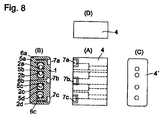
- Fig. 8 is a projection view of the dielectric duplexer, wherein a top view, a left side view, a right side vide, and a rear side view are given in Figs. 8A, 8B, 8C, and 8D, respectively.
- the upper surface shown in Fig. 8 is a surface to be in contact with a mounting substrate.
- substantially parallel though-holes 2a to 2d are formed in a dielectric block 1 having a generally rectangular shape.
- An inner conductor having a thin-film multilayer electrode structure is formed on the inner surface of each through-hole.
- An outer conductor 4 having a thin-film multilayer electrode structure is formed on the four side faces, parallel to the axes of the through-holes, of the dielectric block 1.
- An outer conductor 4' in the form of a single-layer electrode is disposed on an end face, serving as a short-circuited plane, of the dielectric block 1.
- open-end electrodes 5a to 5d are formed which extend continuously from the respective inner conductors.
- coupling electrodes 6a, 6b, and 6c capacitively coupled with adjacent open-end electrodes are also formed.
- signal input/output terminals 7a, 7b, and 7c are formed on this open-circuited end face of the dielectric block 1 such that they continuously extend from the respective coupling electrodes 6a, 6b, and 6c and such that they are electrically isolated from the outer conductor 4.
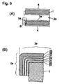
- Fig. 9A is a cross-sectional view of the dielectric duplexer, taken along a plane in which the axis of the through-hole 2a lies and which is perpendicular to the upper surface of the dielectric block 1.
- Fig. 9B is an enlarged view of a part denoted by B in Fig. 9A.
- the inner conductor 3a is formed so as to have a thin-film multilayer electrode structure consisting of thin-film conductive layers 31, thin-film dielectric layers 32, and an outermost conductive layer 33.
- the open-end electrode 5a also has a thin-film multilayer electrode structure each layer of which extends continuously to the end face of the dielectric block 1.
- the two resonators formed with the respective through-holes 2a and 2b are coupled to each other via capacitance between the open-end electrodes 5a and 5b.
- the two resonators formed with the respective through-holes 2c and 2d are coupled to each other via capacitance between the open-end electrodes 5c and 5d.
- the coupling electrode 6a is capacitively coupled with the open-end electrode 5a
- the coupling electrode 6c is capacitively coupled with the open-end electrode 5d.
- the coupling electrode 6b is capacitively coupled with the open-end electrodes 5b and 5c.
- the dielectric duplexer functions as an antenna duplexer in which the signal input/output terminal 7a serves as an external terminal for connection with a transmitting circuit, the signal input/output terminal 7b serves as an external terminal for connection with an antenna, and the signal input/output terminal 7c serves as an external terminal for connection with a receiving circuit.
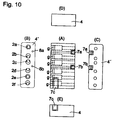
- Figs. 10A, 10B, 10C, 10D, and 10E are a top view, a left side view, a right side vide, a rear side view, and a front view, respectively, of the dielectric duplexer.
- the upper surface shown in Fig. 10 is a surface to be in contact with a mounting substrate.
- substantially parallel though-holes 2a to 2f, 8a, and 8b are formed in a dielectric block a having a generally rectangular shape.
- An inner conductor having a thin-film multilayer electrode structure is formed on the inner surface of each through-hole 2a to 2f, and a non-electrode part g is formed in a region near one open end of each through-hole 2a to 2f.
- An outer conductor 4 having a thin-film multilayer electrode structure is formed on the four side faces, parallel to the axes of the through-holes, of the dielectric block 1.
- An outer conductor 4' in the form of a single-layer electrode is disposed on two end faces, serving as short-circuited planes, of the dielectric block 1.
- Signal input/output terminals 7a and 7b are formed on one open end of each through-hole 8a and 8b such the signal input/output terminals 7a and 7b extend continuously from the inner conductor formed on the inner surface of the through-holes 8a and 8b to the end face and further to the upper surface of the dielectric block 1 and such that the signal input/output terminals 7a and 7b are isolated from the outer electrodes 4 and 4'. Furthermore, a signal input/output terminal 7c isolated from the outer conductor 4 is also formed on the outer surface of the dielectric block 1.
- the two resonators formed with the through-holes 2b and 2c are coupled in a comb line fashion.
- the coupling line holes 8a and 8b are interdigitally coupled with the respective resonators formed with the through-holes 2b and 2c.
- the resonator formed with the through-hole 2a is interdigitally coupled with the coupling line hole 8a.
- a filter having a wide passband is formed with the 2-stage resonator consisting of the through-holes 2b and 2c, and a transmission filter is formed with this wide-band filter and a trap resonator realized by the through-hole 2a.
- Three resonators formed with the through-holes 2d, 2e, and 2f are coupled in a comb line fashion.
- the coupling line hole 8b is interdigitally coupled with the resonator formed with the through-hole 2d.
- the signal input/output terminal 7c is capacitively coupled with the resonator formed with the through-hole 2f.
- reception filter having a band-pass characteristic is formed with the three resonators realized by the through-holes 2d, 2e, and 2f.
- the dielectric duplexer functions as an antenna duplexer in which the signal input/output terminal 7a serves as an external terminal for connection with a transmitting circuit, the signal input/output terminal 7b serves as an external terminal for connection with an antenna, and the signal input/output terminal 7c serves as an external terminal for connection with a receiving circuit.
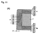
- Figs. 11A and 11B are enlarged cross-sectional views illustrating parts of dielectric blocks of a dielectric filter or a dielectric duplexer.
- Figs. 11A and 11B the cross-sectional structure of a short-circuited end part, similar to the part denoted by C in Fig. 3 or 7, of a dielectric block is shown.
- the structure of an inner conductor 3 formed on the inner surface of a through-hole 2 and that of an outer conductor 4 formed on outer side faces of the dielectric block 1 are similar to those shown in Fig. 3 or 7.
- the respective thin-film conductive layers including the outermost conductive layers are electrically connected together via a single-layer electrode.
- the respective thin-film conductive layers have the common zero potential, and high-frequency currents flowing through the respective thin-film conductive layers have the same phase.
- the effective skin depth is increased. Because the outer electrode 4 on the short-circuited end face also has the thin-film multilayer electrode structure, the current is distributed among the thin-film conductive layers of the outer conductor 4 on the short-circuited end face, and thus the conductor loss at the short-circuited end face is sufficiently reduced.
- the inner conductor 3 on the inner surface of the through-hole 2, the outer conductor 4 on the outer surface of the dielectric block 1, and the outer conductor 4 on the short-circuited end face are all formed with a continuous electrode having a thin-film multilayer structure.
- the high frequency currents flowing through the respective thin-film conductive layers have substantially the same phase, and the effective skin depth is increased. Furthermore, the current is distributed among the thin-film conductive layers of the outer conductor 4 on the short-circuited end face, and thus the conductor loss at the short-circuited end face is also sufficiently reduced.
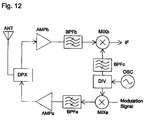
- the communication device includes a transmission/reception antenna ANT, a duplexer DPX, band-pass filters BPFa, BPFb, and BPFc, amplifiers AMPa and AMPb, mixers MIXa and MIXb, an oscillator OSC, and a frequency divider (synthesizer) DIV.
- the mixer MIXa modulates the frequency signal output from the frequency divider DIV in accordance with a modulation signal.
- the band-pass filter BPFa passes only signal components within the transmission frequency band.
- the amplifier AMPa amplifies the power of the signal output from the band-pass filter BPFa.
- the amplified signal is supplied to the antenna ANT via the duplexer DPX and transmitted from the antenna ANT.
- the amplifier AMPb amplifies a signal output from the duplexer DPX.
- the band-pass filter BPFb passes only signal components within the reception frequency band.
- the mixer MIXb mixes the frequency signal output from the band-pass filter BPFc with the received signal and outputs an intermediate frequency signal IF.
- a dielectric duplexer having any one of the structures shown in Fig. 8, 10, and 11 may be employed as the duplexer DPX shown in Fig. 12.
- a dielectric filter having any one of the structures shown in Figs. 1 to 7 and 11 may be employed as the band-pass filters BPFa, BPFb, and BPFc.
- electrodes are formed on the inner and outer surfaces of a single dielectric block having a rectangular shape.
- a dielectric resonator, a dielectric filter, or a dielectric duplexer, having a similar structure may be produced by adhesively combining two or more dielectric blocks having electrodes formed at particular locations.
- the thin-film multilayer electrodes may be produced by alternately forming conductive layers and dielectric layers into a multilayer structure by means of a physical or chemical film deposition technique such as sputtering, vacuum evaporation, CVD, laser abrasion, or ion plating.
- the present invention provides great advantages. That is, in an aspect of the present invention, at least a part of at least one of the inner conductor and the outer conductor has the thin-film multilayer electrode structure formed by alternately disposing thin-film conductive layers with a thickness smaller than the skin depth at the operating frequency and thin-film dielectric layers with a particular dielectric constant, thereby increasing the effective cross-sectional areas of the inner and outer conductors and thus reducing the conductor losses.
- This allows a dielectric resonator, a dielectric filter, and a dielectric duplexer, having a low-loss characteristic, to be realized.
- a communication device having a small size and a high power efficiency can also be realized.
- a through-hole is formed between two opposing end faces of a dielectric block, wherein one of the two opposing end faces of the dielectric block acts as an open-circuited end face and the other end face acts as a short-circuited end face.
- the short-circuited end face is covered with an outer conductor a having a single-layer electrode structure with a thickness greater than the skin depth at the operating frequency.
- the outer conductor disposed on side faces other than the short-circuited end face has the thin-film multilayer electrode structure.
- a plurality of through-holes are formed in a dielectric block, and inner conductors are formed on the inner surfaces of the through-holes such that closest parts of inner conductors have the thin-film multilayer electrode structure.
- the thin-film multilayer electrodes are provided at location where the currents are concentrated, the insertion loss of the dielectric filter is efficiently improved.
Landscapes
- Physics & Mathematics (AREA)
- Electromagnetism (AREA)
- Control Of Motors That Do Not Use Commutators (AREA)
Abstract
Description
Claims (11)
- A dielectric resonator comprising:a dielectric block (1);an inner conductor (3; 3a, 3b) formed on the inner surface of a through-hole (2; 2a, 2b; 2a-2d; 2a-2f)extending from one end face to the opposite end face of said dielectric block (1); andan outer conductor (4) formed on the outer surface of said dielectric block (1), whereinat least a part of at least one of said inner conductor (3; 3a, 3b) and said outer conductor (4) has a thin-film multilayer electrode structure formed by alternately disposing thin-film conductive layers (31, 41, 33, 43) with a thickness smaller than the skin depth at an operating frequency and thin-film dielectric layers (32, 42) with a particular dielectric constant.
- A dielectric resonator according to Claim 1, wherein said outer conductor (4) is formed so as to have said thin-film multilayer electrode structure.
- A dielectric resonator according to Claim 1 or 2, wherein said inner conductor (3) is formed so as to have said thin-film multilayer electrode structure.
- A dielectric resonator according to Claim 1, 2 or 3, wherein said one end face is formed so as to act as an open-circuited end face and said opposite end face is formed so as to act as a short-circuited end face, a part (4') of said outer conductor (4) on said short-circuited end face is formed so as to have a single-layer electrode structure, and the part of the outer conductor (4) other than the part (4') on said short-circuited end face is formed so as to have the thin-film multilayer electrode structure.
- A dielectric resonator according to Claim 4, wherein the part (4') of the outer conductor on said short-circuited end face has a thickness equal to or greater than 3 times the skin depth at said operating frequency.
- A dielectric resonator according to one of Claims 1 to 5, wherein said through-hole (2a, 2b; 2a-2d; 2a-2f) includes a small-diameter part having a small hole diameter and a large-diameter part having a large hole diameter.
- A dielectric filter comprising:a dielectric block (1) according to one of Claims 1 to 6; andexternal terminals (7a, 7b) serving as high-frequency signal input/output terminals disposed on the outer surface of said dielectric block (1).
- A dielectric filter according to Claim 7, wherein said dielectric block (1) has a plurality of said through-holes (2a, 2b).
- A dielectric filter according to Claim 8, wherein, of the inner conductors (3a, 3b) formed on the inner surfaces of adjacent through-holes (2a, 2b), closest parts of inner conductors are formed so as to have said thin-film multilayer electrode structure.
- A dielectric duplexer comprising:a dielectric filter according to one of Claims 7 to 9;an external terminal (7b) for connection with an antenna;an external terminal (7c) for connection with a receiving circuit; andan external terminal (7a) for connection with a transmitting circuit,said external terminals (7a, 7b, 7c) being disposed on the outer surface of said dielectric block (1).
- A communication device including a dielectric filter according to one of Claims 7 to 9 or a dielectric duplexer according to Claim 10.
Applications Claiming Priority (4)
| Application Number | Priority Date | Filing Date | Title |
|---|---|---|---|
| JP31465899 | 1999-11-05 | ||
| JP31465899 | 1999-11-05 | ||
| JP2000256191A JP2001196817A (en) | 1999-11-05 | 2000-08-25 | Dielectric resonator, dielectric filter, dielectric duplexer and communication apparatus |
| JP2000256191 | 2000-08-25 |
Publications (3)
| Publication Number | Publication Date |
|---|---|
| EP1102344A2 true EP1102344A2 (en) | 2001-05-23 |
| EP1102344A3 EP1102344A3 (en) | 2002-03-20 |
| EP1102344B1 EP1102344B1 (en) | 2008-04-09 |
Family
ID=26568017
Family Applications (1)
| Application Number | Title | Priority Date | Filing Date |
|---|---|---|---|
| EP00122900A Expired - Lifetime EP1102344B1 (en) | 1999-11-05 | 2000-10-20 | Dielectric resonator, dielectric filter, dielectric duplexer, and communication device |
Country Status (6)
| Country | Link |
|---|---|
| US (1) | US6556101B1 (en) |
| EP (1) | EP1102344B1 (en) |
| JP (1) | JP2001196817A (en) |
| KR (1) | KR100352574B1 (en) |
| CN (1) | CN1159798C (en) |
| DE (1) | DE60038528T2 (en) |
Cited By (1)
| Publication number | Priority date | Publication date | Assignee | Title |
|---|---|---|---|---|
| EP1684374A1 (en) * | 2005-01-20 | 2006-07-26 | M/A-Com, Inc. | Dielectric resonator with variable diameter through hole and circuit with such dielectric resonators |
Families Citing this family (46)
| Publication number | Priority date | Publication date | Assignee | Title |
|---|---|---|---|---|
| US6703912B2 (en) * | 2001-08-10 | 2004-03-09 | Sanyo Electric Co., Ltd. | Dielectric resonator devices, dielectric filters and dielectric duplexers |
| JP2003174306A (en) | 2001-09-27 | 2003-06-20 | Murata Mfg Co Ltd | Resonator, filter, duplexer, and high-frequency circuit apparatus |
| KR100811783B1 (en) * | 2002-05-08 | 2008-03-07 | 엘지이노텍 주식회사 | Antenna Switch Using Low Temperature Plasticity Ceramic |
| US20040085165A1 (en) * | 2002-11-05 | 2004-05-06 | Yung-Rung Chung | Band-trap filter |
| US9208942B2 (en) * | 2009-03-09 | 2015-12-08 | Nucurrent, Inc. | Multi-layer-multi-turn structure for high efficiency wireless communication |
| US11476566B2 (en) | 2009-03-09 | 2022-10-18 | Nucurrent, Inc. | Multi-layer-multi-turn structure for high efficiency wireless communication |
| US9439287B2 (en) | 2009-03-09 | 2016-09-06 | Nucurrent, Inc. | Multi-layer wire structure for high efficiency wireless communication |
| US9232893B2 (en) | 2009-03-09 | 2016-01-12 | Nucurrent, Inc. | Method of operation of a multi-layer-multi-turn structure for high efficiency wireless communication |
| US9306358B2 (en) | 2009-03-09 | 2016-04-05 | Nucurrent, Inc. | Method for manufacture of multi-layer wire structure for high efficiency wireless communication |
| US9300046B2 (en) * | 2009-03-09 | 2016-03-29 | Nucurrent, Inc. | Method for manufacture of multi-layer-multi-turn high efficiency inductors |
| US9444213B2 (en) | 2009-03-09 | 2016-09-13 | Nucurrent, Inc. | Method for manufacture of multi-layer wire structure for high efficiency wireless communication |
| EP2845263B1 (en) * | 2012-05-01 | 2019-09-25 | Nanoton, Inc. | Radio frequency (rf) conductive medium |
| CN103840240B (en) * | 2012-11-20 | 2020-03-17 | 深圳光启创新技术有限公司 | Resonant cavity, filter device and electromagnetic wave equipment |
| CN103165969B (en) * | 2012-11-20 | 2014-04-16 | 深圳光启创新技术有限公司 | Harmonic oscillator, resonant cavity, wave filter component and electromagnetic wave equipment |
| EP3370300B1 (en) | 2013-04-16 | 2021-06-09 | Huawei Technologies Co., Ltd. | Dielectric resonator, dielectric filter, and fabrication method |
| KR101588874B1 (en) * | 2014-03-28 | 2016-01-27 | 주식회사 이너트론 | Resonator and filter having the same |
| KR101561285B1 (en) * | 2014-03-28 | 2015-10-20 | 주식회사 이너트론 | Multi-band filter |
| US9941743B2 (en) | 2015-08-07 | 2018-04-10 | Nucurrent, Inc. | Single structure multi mode antenna having a unitary body construction for wireless power transmission using magnetic field coupling |
| US9941729B2 (en) | 2015-08-07 | 2018-04-10 | Nucurrent, Inc. | Single layer multi mode antenna for wireless power transmission using magnetic field coupling |
| US11205848B2 (en) | 2015-08-07 | 2021-12-21 | Nucurrent, Inc. | Method of providing a single structure multi mode antenna having a unitary body construction for wireless power transmission using magnetic field coupling |
| US9948129B2 (en) | 2015-08-07 | 2018-04-17 | Nucurrent, Inc. | Single structure multi mode antenna for wireless power transmission using magnetic field coupling having an internal switch circuit |
| US9960628B2 (en) | 2015-08-07 | 2018-05-01 | Nucurrent, Inc. | Single structure multi mode antenna having a single layer structure with coils on opposing sides for wireless power transmission using magnetic field coupling |
| US10658847B2 (en) | 2015-08-07 | 2020-05-19 | Nucurrent, Inc. | Method of providing a single structure multi mode antenna for wireless power transmission using magnetic field coupling |
| US10063100B2 (en) | 2015-08-07 | 2018-08-28 | Nucurrent, Inc. | Electrical system incorporating a single structure multimode antenna for wireless power transmission using magnetic field coupling |
| US10636563B2 (en) | 2015-08-07 | 2020-04-28 | Nucurrent, Inc. | Method of fabricating a single structure multi mode antenna for wireless power transmission using magnetic field coupling |
| US9960629B2 (en) | 2015-08-07 | 2018-05-01 | Nucurrent, Inc. | Method of operating a single structure multi mode antenna for wireless power transmission using magnetic field coupling |
| US9941590B2 (en) | 2015-08-07 | 2018-04-10 | Nucurrent, Inc. | Single structure multi mode antenna for wireless power transmission using magnetic field coupling having magnetic shielding |
| WO2017031348A1 (en) | 2015-08-19 | 2017-02-23 | Nucurrent, Inc. | Multi-mode wireless antenna configurations |
| US11011915B2 (en) | 2016-08-26 | 2021-05-18 | Nucurrent, Inc. | Method of making a wireless connector transmitter module |
| US10468733B2 (en) * | 2016-11-08 | 2019-11-05 | LGS Innovations LLC | Ceramic block filter having through holes of specific shapes |
| EP3552298A4 (en) | 2016-12-09 | 2020-01-15 | NuCurrent, Inc. | SUBSTRATE CONFIGURED TO FACILITATE METAL ENERGY TRANSFER THROUGH NEAR-FIELD MAGNETIC COUPLING |
| US11177695B2 (en) | 2017-02-13 | 2021-11-16 | Nucurrent, Inc. | Transmitting base with magnetic shielding and flexible transmitting antenna |
| US10651201B2 (en) * | 2017-04-05 | 2020-05-12 | Samsung Electronics Co., Ltd. | Integrated circuit including interconnection and method of fabricating the same, the interconnection including a pattern shaped and/or a via disposed for mitigating electromigration |
| US11277028B2 (en) | 2017-05-26 | 2022-03-15 | Nucurrent, Inc. | Wireless electrical energy transmission system for flexible device orientation |
| CN107706488B (en) * | 2017-09-30 | 2020-12-11 | 厦门松元电子有限公司 | Multistage resonance band-pass filter of structural type |
| US11227712B2 (en) | 2019-07-19 | 2022-01-18 | Nucurrent, Inc. | Preemptive thermal mitigation for wireless power systems |
| US11271430B2 (en) | 2019-07-19 | 2022-03-08 | Nucurrent, Inc. | Wireless power transfer system with extended wireless charging range |
| JP7211533B2 (en) * | 2019-11-29 | 2023-01-24 | 株式会社村田製作所 | Dielectric resonators, dielectric filters, and multiplexers |
| US11056922B1 (en) | 2020-01-03 | 2021-07-06 | Nucurrent, Inc. | Wireless power transfer system for simultaneous transfer to multiple devices |
| US11283303B2 (en) | 2020-07-24 | 2022-03-22 | Nucurrent, Inc. | Area-apportioned wireless power antenna for maximized charging volume |
| US11876386B2 (en) | 2020-12-22 | 2024-01-16 | Nucurrent, Inc. | Detection of foreign objects in large charging volume applications |
| US11881716B2 (en) | 2020-12-22 | 2024-01-23 | Nucurrent, Inc. | Ruggedized communication for wireless power systems in multi-device environments |
| US11695302B2 (en) | 2021-02-01 | 2023-07-04 | Nucurrent, Inc. | Segmented shielding for wide area wireless power transmitter |
| JP7582451B2 (en) | 2021-03-29 | 2024-11-13 | 株式会社村田製作所 | Dielectric Filter |
| US11831174B2 (en) | 2022-03-01 | 2023-11-28 | Nucurrent, Inc. | Cross talk and interference mitigation in dual wireless power transmitter |
| US12003116B2 (en) | 2022-03-01 | 2024-06-04 | Nucurrent, Inc. | Wireless power transfer system for simultaneous transfer to multiple devices with cross talk and interference mitigation |
Family Cites Families (8)
| Publication number | Priority date | Publication date | Assignee | Title |
|---|---|---|---|---|
| BE507158A (en) * | 1951-03-07 | |||
| US2831921A (en) * | 1952-09-11 | 1958-04-22 | Bell Telephone Labor Inc | Loaded laminated conductor |
| WO1995006336A1 (en) * | 1993-08-27 | 1995-03-02 | Murata Manufacturing Co., Ltd. | Thin-film multilayer electrode of high frequency electromagnetic field coupling |
| JP3362535B2 (en) | 1994-12-14 | 2003-01-07 | 株式会社村田製作所 | High frequency electromagnetic field coupling type thin film laminated electrode, high frequency transmission line, high frequency resonator, high frequency filter, high frequency device, and method of setting film thickness of high frequency electromagnetic field coupling type thin film laminated electrode |
| JPH08191208A (en) | 1995-01-06 | 1996-07-23 | Murata Mfg Co Ltd | Method for adjusting resonance frequency of high frequency resonator |
| JP3314594B2 (en) * | 1995-09-22 | 2002-08-12 | 松下電器産業株式会社 | High frequency circuit electrode, transmission line and resonator using the same |
| JPH10220302A (en) | 1997-02-07 | 1998-08-18 | Hino Motors Ltd | Natural gas engine |
| JPH10335906A (en) * | 1997-03-31 | 1998-12-18 | Murata Mfg Co Ltd | Dielectric filter, dielectric duplexer, and communication equipment device |
-
2000
- 2000-08-25 JP JP2000256191A patent/JP2001196817A/en active Pending
- 2000-10-20 DE DE60038528T patent/DE60038528T2/en not_active Expired - Lifetime
- 2000-10-20 EP EP00122900A patent/EP1102344B1/en not_active Expired - Lifetime
- 2000-11-04 KR KR1020000065364A patent/KR100352574B1/en not_active Expired - Lifetime
- 2000-11-06 CN CNB001328360A patent/CN1159798C/en not_active Expired - Lifetime
- 2000-11-06 US US09/707,264 patent/US6556101B1/en not_active Expired - Lifetime
Cited By (2)
| Publication number | Priority date | Publication date | Assignee | Title |
|---|---|---|---|---|
| EP1684374A1 (en) * | 2005-01-20 | 2006-07-26 | M/A-Com, Inc. | Dielectric resonator with variable diameter through hole and circuit with such dielectric resonators |
| US7388457B2 (en) | 2005-01-20 | 2008-06-17 | M/A-Com, Inc. | Dielectric resonator with variable diameter through hole and filter with such dielectric resonators |
Also Published As
| Publication number | Publication date |
|---|---|
| KR20010051449A (en) | 2001-06-25 |
| EP1102344A3 (en) | 2002-03-20 |
| CN1159798C (en) | 2004-07-28 |
| CN1301055A (en) | 2001-06-27 |
| DE60038528T2 (en) | 2009-06-10 |
| JP2001196817A (en) | 2001-07-19 |
| KR100352574B1 (en) | 2002-09-12 |
| DE60038528D1 (en) | 2008-05-21 |
| EP1102344B1 (en) | 2008-04-09 |
| US6556101B1 (en) | 2003-04-29 |
Similar Documents
| Publication | Publication Date | Title |
|---|---|---|
| EP1102344B1 (en) | Dielectric resonator, dielectric filter, dielectric duplexer, and communication device | |
| US6426725B2 (en) | Antenna device and communication device | |
| EP0917236A2 (en) | High-frequency transmission line, dielectric resonator, filter, duplexer, and communication device | |
| JP2001077609A (en) | Dielectric resonator, inductor, capacitor, dielectric filter, oscillator, dielectric duplexer, and communications equipment | |
| US6445263B1 (en) | Dielectric resonator, dielectric filter, duplexer, and communication device | |
| JP3498649B2 (en) | Dielectric filter, duplexer and communication device | |
| US6549093B2 (en) | Dielectric filter, duplexer, and communication apparatus incorporating the same | |
| EP1025608B1 (en) | Duplexer with stepped impedance resonators | |
| JP3348658B2 (en) | Dielectric filter, composite dielectric filter, antenna duplexer, and communication device | |
| JP3478244B2 (en) | Coaxial resonator, filter, duplexer and communication device | |
| EP1612881B1 (en) | Dielectric filter, dielectric duplexer, and communication apparatus incorporating the same | |
| EP1294042B1 (en) | Dielectric filter, dielectric duplexer, and communication device | |
| US6661310B2 (en) | Dielectric duplexer and communication apparatus | |
| KR100282567B1 (en) | High Frequency Filter Using Closed Loop Resonator | |
| JP2001007605A (en) | Dielectric filter, dielectric duplexer and communication unit | |
| KR100299055B1 (en) | Microwave filter using closed loop resonators | |
| US20020145491A1 (en) | Dielectric filter, dielectric duplexer, and communications equipment |
Legal Events
| Date | Code | Title | Description |
|---|---|---|---|
| PUAI | Public reference made under article 153(3) epc to a published international application that has entered the european phase |
Free format text: ORIGINAL CODE: 0009012 |
|
| 17P | Request for examination filed |
Effective date: 20001020 |
|
| AK | Designated contracting states |
Kind code of ref document: A2 Designated state(s): AT BE CH CY DE DK ES FI FR GB GR IE IT LI LU MC NL PT SE Kind code of ref document: A2 Designated state(s): DE FR GB |
|
| AX | Request for extension of the european patent |
Free format text: AL;LT;LV;MK;RO;SI |
|
| PUAL | Search report despatched |
Free format text: ORIGINAL CODE: 0009013 |
|
| AK | Designated contracting states |
Kind code of ref document: A3 Designated state(s): AT BE CH CY DE DK ES FI FR GB GR IE IT LI LU MC NL PT SE |
|
| AX | Request for extension of the european patent |
Free format text: AL;LT;LV;MK;RO;SI |
|
| AKX | Designation fees paid |
Free format text: DE FR GB |
|
| RAP1 | Party data changed (applicant data changed or rights of an application transferred) |
Owner name: MURATA MANUFACTURING CO., LTD. |
|
| GRAP | Despatch of communication of intention to grant a patent |
Free format text: ORIGINAL CODE: EPIDOSNIGR1 |
|
| GRAS | Grant fee paid |
Free format text: ORIGINAL CODE: EPIDOSNIGR3 |
|
| GRAA | (expected) grant |
Free format text: ORIGINAL CODE: 0009210 |
|
| AK | Designated contracting states |
Kind code of ref document: B1 Designated state(s): DE FR GB |
|
| REG | Reference to a national code |
Ref country code: GB Ref legal event code: FG4D |
|
| REF | Corresponds to: |
Ref document number: 60038528 Country of ref document: DE Date of ref document: 20080521 Kind code of ref document: P |
|
| EN | Fr: translation not filed | ||
| PLBE | No opposition filed within time limit |
Free format text: ORIGINAL CODE: 0009261 |
|
| STAA | Information on the status of an ep patent application or granted ep patent |
Free format text: STATUS: NO OPPOSITION FILED WITHIN TIME LIMIT |
|
| 26N | No opposition filed |
Effective date: 20090112 |
|
| PG25 | Lapsed in a contracting state [announced via postgrant information from national office to epo] |
Ref country code: FR Free format text: LAPSE BECAUSE OF FAILURE TO SUBMIT A TRANSLATION OF THE DESCRIPTION OR TO PAY THE FEE WITHIN THE PRESCRIBED TIME-LIMIT Effective date: 20090130 |
|
| GBPC | Gb: european patent ceased through non-payment of renewal fee |
Effective date: 20081020 |
|
| PG25 | Lapsed in a contracting state [announced via postgrant information from national office to epo] |
Ref country code: GB Free format text: LAPSE BECAUSE OF NON-PAYMENT OF DUE FEES Effective date: 20081020 |
|
| PGFP | Annual fee paid to national office [announced via postgrant information from national office to epo] |
Ref country code: DE Payment date: 20191021 Year of fee payment: 20 |
|
| REG | Reference to a national code |
Ref country code: DE Ref legal event code: R071 Ref document number: 60038528 Country of ref document: DE |