EP1100194A2 - Surface acoustic wave filter - Google Patents
Surface acoustic wave filter Download PDFInfo
- Publication number
- EP1100194A2 EP1100194A2 EP00124233A EP00124233A EP1100194A2 EP 1100194 A2 EP1100194 A2 EP 1100194A2 EP 00124233 A EP00124233 A EP 00124233A EP 00124233 A EP00124233 A EP 00124233A EP 1100194 A2 EP1100194 A2 EP 1100194A2
- Authority
- EP
- European Patent Office
- Prior art keywords
- surface acoustic
- acoustic wave
- substrate
- saw
- wave filter
- Prior art date
- Legal status (The legal status is an assumption and is not a legal conclusion. Google has not performed a legal analysis and makes no representation as to the accuracy of the status listed.)
- Withdrawn
Links
Images




Classifications
-
- H—ELECTRICITY
- H03—ELECTRONIC CIRCUITRY
- H03H—IMPEDANCE NETWORKS, e.g. RESONANT CIRCUITS; RESONATORS
- H03H9/00—Networks comprising electromechanical or electro-acoustic elements; Electromechanical resonators
- H03H9/02—Details
- H03H9/02535—Details of surface acoustic wave devices
- H03H9/02637—Details concerning reflective or coupling arrays
- H03H9/02669—Edge reflection structures, i.e. resonating structures without metallic reflectors, e.g. Bleustein-Gulyaev-Shimizu [BGS], shear horizontal [SH], shear transverse [ST], Love waves devices
- H03H9/02677—Edge reflection structures, i.e. resonating structures without metallic reflectors, e.g. Bleustein-Gulyaev-Shimizu [BGS], shear horizontal [SH], shear transverse [ST], Love waves devices having specially shaped edges, e.g. stepped, U-shaped edges
-
- H—ELECTRICITY
- H03—ELECTRONIC CIRCUITRY
- H03H—IMPEDANCE NETWORKS, e.g. RESONANT CIRCUITS; RESONATORS
- H03H9/00—Networks comprising electromechanical or electro-acoustic elements; Electromechanical resonators
- H03H9/02—Details
- H03H9/02535—Details of surface acoustic wave devices
- H03H9/02614—Treatment of substrates, e.g. curved, spherical, cylindrical substrates ensuring closed round-about circuits for the acoustical waves
- H03H9/02622—Treatment of substrates, e.g. curved, spherical, cylindrical substrates ensuring closed round-about circuits for the acoustical waves of the surface, including back surface
-
- H—ELECTRICITY
- H03—ELECTRONIC CIRCUITRY
- H03H—IMPEDANCE NETWORKS, e.g. RESONANT CIRCUITS; RESONATORS
- H03H9/00—Networks comprising electromechanical or electro-acoustic elements; Electromechanical resonators
- H03H9/02—Details
- H03H9/02535—Details of surface acoustic wave devices
- H03H9/02637—Details concerning reflective or coupling arrays
- H03H9/02685—Grating lines having particular arrangements
- H03H9/02716—Tilted, fan shaped or slanted grating lines
-
- H—ELECTRICITY
- H03—ELECTRONIC CIRCUITRY
- H03H—IMPEDANCE NETWORKS, e.g. RESONANT CIRCUITS; RESONATORS
- H03H9/00—Networks comprising electromechanical or electro-acoustic elements; Electromechanical resonators
- H03H9/02—Details
- H03H9/02535—Details of surface acoustic wave devices
- H03H9/02637—Details concerning reflective or coupling arrays
- H03H9/02779—Continuous surface reflective arrays
-
- H—ELECTRICITY
- H03—ELECTRONIC CIRCUITRY
- H03H—IMPEDANCE NETWORKS, e.g. RESONANT CIRCUITS; RESONATORS
- H03H9/00—Networks comprising electromechanical or electro-acoustic elements; Electromechanical resonators
- H03H9/02—Details
- H03H9/02535—Details of surface acoustic wave devices
- H03H9/02637—Details concerning reflective or coupling arrays
- H03H9/02795—Multi-strip couplers as track changers
-
- H—ELECTRICITY
- H03—ELECTRONIC CIRCUITRY
- H03H—IMPEDANCE NETWORKS, e.g. RESONANT CIRCUITS; RESONATORS
- H03H9/00—Networks comprising electromechanical or electro-acoustic elements; Electromechanical resonators
- H03H9/46—Filters
- H03H9/64—Filters using surface acoustic waves
- H03H9/6423—Means for obtaining a particular transfer characteristic
- H03H9/6433—Coupled resonator filters
-
- H—ELECTRICITY
- H03—ELECTRONIC CIRCUITRY
- H03H—IMPEDANCE NETWORKS, e.g. RESONANT CIRCUITS; RESONATORS
- H03H9/00—Networks comprising electromechanical or electro-acoustic elements; Electromechanical resonators
- H03H9/46—Filters
- H03H9/64—Filters using surface acoustic waves
- H03H9/6423—Means for obtaining a particular transfer characteristic
- H03H9/6433—Coupled resonator filters
- H03H9/6436—Coupled resonator filters having one acoustic track only
Definitions
- This invention relates to a surface acoustic wave filter comprising at least one comb shaped interdigital electrode mounted on a piezoelectric substrate, particularly a surface acoustic wave device which can be made smaller along the direction of propagation of surface acoustic waves than that of the prior art.
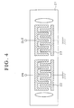
- FIG. 4 shows an example of the configuration of a transversal (or transmission) SAW filter of the prior art.
- the size along the left and right direction of a chip 21, that is, the direction of propagation of surface acoustic waves, is inevitably larger than the sum of the lengths of the input IDT 22 and the output IDT 23, and therefore the miniaturization of the chip is restricted.
- Figure 5 shows a prior art Published Japanese translation No. Hei 5-501486 of PCT International Publication in which oblique metal grating reflectors 34 and 35 are mounted on a transversal SAW filter to reflect a SAW.
- the dimension along the left and right direction of the chip can be reduced by the way in which the SAW is reflected.
- the absolute value of the reflection coefficient of a metal reflector is generally very small, many metal reflectors are usually necessary to achieve a sufficient amount of reflection, and as a result the miniaturization of the chip is restricted.
- a cut surface of a chip is used as a reflection edge surface in a resonator type SAW filter.
- the reflection of a SAW from reflection surfaces 43 and 44 which are cut surfaces of the left and right edges of a chip, is utilized and standing waves are formed along the direction of the arrows in the figure, such that the SAW filter functions as one port resonator.
- a required condition to form a resonator is that the SAW incident on the reflection surface 43 and the SAW required must be in phase.
- the distance between the reflection surface (cut surface) and an electrode 42 must be formed with very high precision (at the micrometer level), resulting in the problem that the chip is difficult to produce.
- the purpose of the present invention is to provide a SAW filter in which a transversal type IDT, which does not resonate in response to the response the generation and reception of a SAW, is used, and in which it is not necessary that the distance between a reflection edge surface and an electrode be formed with very high precision; therefore the formation of a reflection surface is simple, unused regions on a chip can be reduced in comparison with the prior art, and a SAW filter, provided with a small chip which is a constituent element of a SAW device, can be manufactured
- a transversal type surface acoustic wave filter as claimed in claim1 comprises: an input interdigital transducer (IDT), which is comprised of a pair of comb electrodes whose respective electrode fingers are interdigitally formed; substrate boundary surfaces which formed at an angle to a wave front of a propagating surface acoustic wave generated in said input IDT; an output IDT, which is comprised of a pair of comb electrodes whose respective electrode fingers are interdigitally formed; wherein said input and output IDTs and said substrate boundary surfaces are all formed on a piezoelectric substrate; and wherein said input and output IDTs are arranged in parallel and in close proximity to each other along the longitudinal direction of the electrode fingers of said IDTs, and are arranged such that the input and output sides of each IDT are oriented in a direction perpendicular to the longitudinal direction of said electrode fingers.
- IDT input interdigital transducer
- a transversal type surface acoustic wave filter as claimed in claim 2 is characterized in that said substrate boundary surfaces are step shaped, and the height of the step d of said step shaped substrate boundary surfaces is ⁇ d ⁇ 5 ⁇ , where ⁇ is a wavelength of the SAW.
- a transversal type surface acoustic wave filter as claimed in claim 3 is characterized in that said substrate boundary surfaces are formed at an angle of 45 degrees to the wave front of said surface acoustic wave, and said surface acoustic wave only has displacement components parallel to said substrate.
- a transversal type surface acoustic wave filter as claimed in claim 4 is characterized in that said surface acoustic wave, which only has displacement components parallel to said substrate, is a BGS wave.
- a transversal type surface acoustic wave filter as claimed in claim 5 is characterized in that said surface acoustic wave, which only has displacement components parallel to said substrate, is a LOVE wave.
- a transversal type surface acoustic wave filter as claimed in claim 6 is characterized in that said surface acoustic wave, which only has displacement components parallel to said substrate, is an SH wave.
- a transversal type surface acoustic wave filter as claimed in claim 7 is characterized in that said surface acoustic wave, which has only displacement components parallel to said substrate, is an SSBW.
- Figure 1 shows a surface acoustic wave filter of a first embodiment of the present invention.
- Figure 2 shows a surface acoustic wave filter of a second embodiment of the present invention.
- Figure 3 shows a surface acoustic wave filter of a third embodiment of the present invention.
- Figure 4 shows a surface acoustic wave filter of a prior art.
- Figure 5 shows a surface acoustic wave filter of a second prior art.
- Figure 6 shows a surface acoustic wave filter of a third prior art.
- Figure 1 shows a first example of a configuration of a SAW filter according to the present invention.
- a SAW generated by an input IDT 12 is reflected from an oblique reflection surface 15 which is a step formed on the right part of a chip 11 at an oblique angle to a wave front of the input SAW, propagates along an oblique angle on the chip, as shown by an arrow 17 in the figure, is reflected again from an oblique reflection surface 14 which is a step formed on the left part of the chip, and is received by an output IDT 13.
- Figure 1 shows a transversal type SAW fiber formed on a rectangular piezoelectric substrate according to the present invention.
- Figures 1(A), 1(B), and 1(C) are a top view, a side view as seen from the top portion of the figure, and a side view as seen from the bottom portion of the figure, respectively.
- a SAW generated by the input IDT 12 propagates in both directions 16 and 19 as shown in Figure 1.
- a SAW propagating along the direction 16 is reflected from a step shaped reflection surface 15 which is formed at an oblique angle to the wave front of the input SAW on the right part of the chip and propagates along an oblique direction 17 on the chip.
- the SAW is then reflected again from a step shaped reflection surface 14 on the left part of the chip, which is formed parallel to the step shaped reflection surface 15, propagates along a direction 18 and is received by the output IDT 13. Because the propagating energy of the SAW is concentrated in a location within a few multiples of ⁇ from the substrate surface, a good value for the height of the step d is about ⁇ d ⁇ 5 ⁇ , where ⁇ is a wavelength of the SAW.
- the reflection surfaces 14 and 15 can be formed by chemical processes such as etching or by machining processes such as dicing. Because SAWs propagating along the directions 19 and 20 are not wanted in the present embodiment, absorbing parts 25 are provided on the chip in order to attenuate the SAW.
- the loss in reflection at the concentrated and oblique step shaped reflection surfaces 14 and 15 of the present invention is lower than that of a distributed type reflector composed of an oblique metal grating of the prior art shown in Figure 4. Because the reflection factor for each oblique metal grating is roughly a few percent in the prior art shown in Figure 4, a large quantity of SAW energy penetrates the oblique metal reflector and leaks out when there is a small number of gratings, resulting in a large loss in reflection. Several tens or hundreds of gratings are necessary in order to reduce the loss in reflection, and as a result, miniaturization is restricted.
- Figure 2 shows a second embodiment of the present invention. Cut surfaces 54 and 55 of a chip are directly used as oblique reflection surfaces in the configuration of this second embodiment, while the oblique step shaped reflection surfaces are formed by chemically and mechanically machining a rectangular chip in the first embodiment shown in Figure 1. In this second embodiment, it is possible to achieve a greater degree of miniaturization because unused regions on the chip are fewer than those of the first embodiment.
- Figure 3 shows a third embodiment of the present invention.
- this embodiment is a SAW filter in which oblique step shaped reflection surfaces 64 and 65 are formed respectively at the upper and lower halves of one side of a chip (right side in the figure) oriented to the propagating SAW such that the SAW is incident on and reflects from the reflection surfaces at an angle of 45 degrees to the reflection surfaces and the SAW reflects with an angle of 90 degrees, and wherein SAW absorbing parts 25 are formed both at the side opposite the SAW output side 66 of an input IDT 62, and at the side opposite the SAW input side 68 of an output IDT 63.
- the exciting wave is a SAW, such as a BGS wave, a LOVE wave or the like, which only have components of displacement parallel to the substrate, or an SH wave or an SSBW (Surface Skimming Bulk Wave) which are bulk waves that can propagate on the surface of an elastic object to be received by a surface electrode, a mode transformation into longitudinal waves does not occur. For this reason, if these waves are propagated, a low-loss filter can be manufactured.
- an SH wave or an SSB wave because the wave energy is not necessarily concentrated on the surfaces, a structure in which an edge is cut off, as shown in Figure 2, is more appropriate for a reflection surface.
- a BGS wave or an SH wave can be excited if the polarized axis of the substrate is selected so as to be parallel to the electrode finger of the IDT.
- a BGS wave or an SSBW can be generated if a rotating Y substrate is selected.
- a quartz Y substrate with a cutting angle of 70 degrees is selected, a BGS wave can be strongly generated.
- a LOVE wave can propagate if an elastic film is formed in which a LOVE wave propagates at a slower speed than an SH wave.
- a surface acoustic wave filter formed on a piezoelectric substrate according to the present invention has the following characteristics. Because an oblique step shaped reflection surface is provided in order to reflect the SAW, a smaller SAW filter than that used in the prior art can be implemented. Because a concentrated-type total reflection surface is provided, a low-loss filter can be implemented more readily than the prior art provided with distributed-type oblique metal gratings. Because a SAW filter of the present invention is transversal-type, not resonator-type and therefore it is not necessary to form the reflection edge surface with high precision, it is easier to manufacture the SAW filter.
Landscapes
- Physics & Mathematics (AREA)
- Acoustics & Sound (AREA)
- Surface Acoustic Wave Elements And Circuit Networks Thereof (AREA)
Abstract
Description
Claims (7)
- A transversal type surface acoustic wave filter comprising:an input interdigital transducer (IDT) (12, 52, 62), which is comprised of a pair of comb electrodes whose respective electrode fingers are interdigitally formed;substrate boundary surfaces (14, 15, 54, 55, 64, 65) which formed at an angle to a wave front of a propagating surface acoustic wave generated in said input IDT (12, 52, 62);an output IDT (13, 53, 63), which is comprised of a pair of comb electrodes whose respective electrode fingers are interdigitally formed;wherein said input and output IDTs (12, 52, 62; 13, 53, 63) and said substrate boundary surfaces (14, 15, 54, 55, 64, 65) are all formed on a piezoelectric substrate;and wherein said input and output IDTs (12, 52, 62; 13, 53, 63) are arranged in parallel and in close proximity to each other along the longitudinal direction of the electrode fingers of said IDTs (12, 52, 62; 13, 53, 63), and are arranged such that the input and output sides of each IDT (12, 52, 62; 13, 53, 63) are oriented in a direction perpendicular to the longitudinal direction of said electrode fingers.
- A transversal type surface acoustic wave filter as claimed in claim 1, wherein said substrate boundary surfaces (14, 15, 54, 55, 64, 65) are step shaped, and the height of the step d of said step shaped substrate boundary surfaces is λ<d<5 λ, where λ is the wavelength of a SAW.
- A transversal type surface acoustic wave filter as claimed in claim 1, wherein said substrate boundary surfaces (14, 15, 54, 55, 64, 65) are formed at an angle of 45 degrees to the wave front of said surface acoustic wave, and said surface acoustic wave only has displacement components parallel to said substrate.
- A transversal type surface acoustic wave filter as claimed in claim 3, wherein said surface acoustic wave, which only has displacement components parallel to said substrate, is a BGS wave.
- A transversal type surface acoustic wave filter as claimed in claim 3, wherein said surface acoustic wave, which only has displacement components parallel to said substrate, is a LOVE wave.
- A transversal type surface acoustic wave filter as claimed in claim 3, wherein said surface acoustic wave, which only has displacement components parallel to said substrate, is an SH wave.
- A transversal type surface acoustic wave filter as claimed in claim 3, wherein said surface acoustic wave, which only has displacement components parallel to said substrate, is an SSBW.
Applications Claiming Priority (2)
| Application Number | Priority Date | Filing Date | Title |
|---|---|---|---|
| JP31810599 | 1999-11-09 | ||
| JP31810599A JP2001136048A (en) | 1999-11-09 | 1999-11-09 | Surface acoustic wave filter |
Publications (2)
| Publication Number | Publication Date |
|---|---|
| EP1100194A2 true EP1100194A2 (en) | 2001-05-16 |
| EP1100194A3 EP1100194A3 (en) | 2005-06-22 |
Family
ID=18095556
Family Applications (1)
| Application Number | Title | Priority Date | Filing Date |
|---|---|---|---|
| EP00124233A Withdrawn EP1100194A3 (en) | 1999-11-09 | 2000-11-09 | Surface acoustic wave filter |
Country Status (3)
| Country | Link |
|---|---|
| US (1) | US6373167B1 (en) |
| EP (1) | EP1100194A3 (en) |
| JP (1) | JP2001136048A (en) |
Families Citing this family (5)
| Publication number | Priority date | Publication date | Assignee | Title |
|---|---|---|---|---|
| US6699728B2 (en) * | 2000-09-06 | 2004-03-02 | Osram Opto Semiconductors Gmbh | Patterning of electrodes in oled devices |
| JP2002152001A (en) * | 2000-11-09 | 2002-05-24 | Nec Corp | Surface acoustic wave filter and surface acoustic wave filter device |
| KR100535405B1 (en) * | 2003-12-30 | 2005-12-08 | 현대자동차주식회사 | Surface acoustic wave sensor for measuring pressure and temperature for tire |
| KR100778651B1 (en) * | 2006-07-06 | 2007-11-22 | 주식회사 엠디티 | Tire pressure sensing system and tire pressure sensing method |
| JPWO2012114931A1 (en) * | 2011-02-25 | 2014-07-07 | 株式会社村田製作所 | Variable capacitance element and tunable filter |
Family Cites Families (17)
| Publication number | Priority date | Publication date | Assignee | Title |
|---|---|---|---|---|
| JPS4724245A (en) * | 1971-03-10 | 1972-10-16 | ||
| JPS50125655A (en) * | 1974-03-19 | 1975-10-02 | ||
| JPS5444429B2 (en) * | 1974-03-29 | 1979-12-26 | ||
| JPS5444431B2 (en) * | 1974-03-29 | 1979-12-26 | ||
| US4263571A (en) * | 1978-11-15 | 1981-04-21 | Hitachi, Ltd. | Surface acoustic wave filter |
| DE3438246A1 (en) * | 1984-10-18 | 1986-04-24 | Siemens AG, 1000 Berlin und 8000 München | ACOUSTIC WAVE FILTER |
| DE3777023D1 (en) * | 1986-08-29 | 1992-04-09 | Siemens Ag | CONVERTER FOR A FILTER ARRANGEMENT WITH ACOUSTIC SHAFTS. |
| GB8812539D0 (en) | 1988-05-26 | 1988-06-29 | Ici Plc | Preparation of aromatic compounds & derivatives therefor |
| EP0571365B1 (en) | 1989-11-14 | 1994-10-26 | Siemens Aktiengesellschaft | Surface-wave reflector-filter |
| JPH0426211A (en) * | 1990-05-21 | 1992-01-29 | Murata Mfg Co Ltd | Surface wave device |
| JPH0821830B2 (en) * | 1990-07-24 | 1996-03-04 | 株式会社村田製作所 | Surface wave device |
| JPH0969751A (en) | 1995-08-30 | 1997-03-11 | Murata Mfg Co Ltd | Surface acoustic wave filter |
| TW404091B (en) * | 1997-05-16 | 2000-09-01 | Murata Manufacturing Co | Ladder filter having edge-reflection type resonators |
| JPH11150442A (en) | 1997-08-29 | 1999-06-02 | Murata Mfg Co Ltd | Surface acoustic wave filter |
| NO985386L (en) * | 1997-11-20 | 1999-05-21 | Murata Manufacturing Co | Unidirectional transducer for acoustic surface waves, and transversal filter with such transducer |
| US6023122A (en) * | 1999-04-15 | 2000-02-08 | Nortel Networks Corporation | Surface wave devices with tapered transducers |
| JP2001308675A (en) * | 2000-04-26 | 2001-11-02 | Murata Mfg Co Ltd | Surface wave filter and common device, communication device |
-
1999
- 1999-11-09 JP JP31810599A patent/JP2001136048A/en active Pending
-
2000
- 2000-11-07 US US09/706,745 patent/US6373167B1/en not_active Expired - Fee Related
- 2000-11-09 EP EP00124233A patent/EP1100194A3/en not_active Withdrawn
Also Published As
| Publication number | Publication date |
|---|---|
| EP1100194A3 (en) | 2005-06-22 |
| US6373167B1 (en) | 2002-04-16 |
| JP2001136048A (en) | 2001-05-18 |
Similar Documents
| Publication | Publication Date | Title |
|---|---|---|
| US7009468B2 (en) | Surface acoustic wave device and electronic device using the same | |
| US6587016B2 (en) | Surface acoustic wave filter with angled reflection by piezoelectric substrate reflection edges, duplexer, and communication device | |
| KR100198161B1 (en) | Longitudinally coupling acoustic surface wave double mode filter utilizing end-face reflecting waves | |
| EP1732216B1 (en) | Surface acoustic device | |
| KR101913933B1 (en) | Acoustic wave device | |
| US20020044497A1 (en) | Surface acoustic wave device | |
| CN101534106B (en) | Acoustic wave filter | |
| KR102587658B1 (en) | Acoustic wave filter | |
| US6674215B1 (en) | Elastic wave device | |
| US6346761B1 (en) | Surface acoustic wave device capable of suppressing spurious response due to non-harmonic higher-order modes | |
| US6373167B1 (en) | Surface acoustic wave filter | |
| US20100289379A1 (en) | Surface acoustic wave (saw) device | |
| JP2002152003A (en) | Surface acoustic wave filter | |
| JP2021158553A (en) | Elastic wave devices and their manufacturing methods, filters, multiplexers and wafers | |
| US20230117944A1 (en) | Bonded substrate and its manufacturing method | |
| US6147574A (en) | Unidirectional surface acoustic wave transducer and transversal-type saw filter having the same | |
| US6781282B1 (en) | Longitudinally coupled resonator-type surface acoustic wave device | |
| JP2001119266A (en) | Surface wave device | |
| EP0100503B1 (en) | High frequency narrow-band pass multi-mode filter | |
| JPH09116378A (en) | IDT excitation device | |
| KR20040042829A (en) | Surface acoustic wave device preferable for g㎐ band | |
| JP2004007846A (en) | Surface wave resonator | |
| JPH0685604A (en) | Multimode surface acoustic wave filter | |
| JPS6382115A (en) | Surface acoustic wave element | |
| JP2008160669A (en) | Surface acoustic wave device |
Legal Events
| Date | Code | Title | Description |
|---|---|---|---|
| PUAI | Public reference made under article 153(3) epc to a published international application that has entered the european phase |
Free format text: ORIGINAL CODE: 0009012 |
|
| AK | Designated contracting states |
Kind code of ref document: A2 Designated state(s): AT BE CH CY DE DK ES FI FR GB GR IE IT LI LU MC NL PT SE TR |
|
| AX | Request for extension of the european patent |
Free format text: AL;LT;LV;MK;RO;SI |
|
| RAP1 | Party data changed (applicant data changed or rights of an application transferred) |
Owner name: NRS TECHNOLOGIES INC. |
|
| PUAL | Search report despatched |
Free format text: ORIGINAL CODE: 0009013 |
|
| AK | Designated contracting states |
Kind code of ref document: A3 Designated state(s): AT BE CH CY DE DK ES FI FR GB GR IE IT LI LU MC NL PT SE TR |
|
| AX | Request for extension of the european patent |
Extension state: AL LT LV MK RO SI |
|
| RAP1 | Party data changed (applicant data changed or rights of an application transferred) |
Owner name: NIHON DEMPA KOGYO CO., LTD. |
|
| AKX | Designation fees paid |
Designated state(s): DE FR GB |
|
| STAA | Information on the status of an ep patent application or granted ep patent |
Free format text: STATUS: THE APPLICATION IS DEEMED TO BE WITHDRAWN |
|
| 18D | Application deemed to be withdrawn |
Effective date: 20051223 |