EP1099973A2 - Integrated optoelectronic devices having pop-up mirrors therein and methods of forming and operating same - Google Patents
Integrated optoelectronic devices having pop-up mirrors therein and methods of forming and operating same Download PDFInfo
- Publication number
- EP1099973A2 EP1099973A2 EP00309416A EP00309416A EP1099973A2 EP 1099973 A2 EP1099973 A2 EP 1099973A2 EP 00309416 A EP00309416 A EP 00309416A EP 00309416 A EP00309416 A EP 00309416A EP 1099973 A2 EP1099973 A2 EP 1099973A2
- Authority
- EP
- European Patent Office
- Prior art keywords
- mirror
- backing layer
- layer
- substrate
- forming
- Prior art date
- Legal status (The legal status is an assumption and is not a legal conclusion. Google has not performed a legal analysis and makes no representation as to the accuracy of the status listed.)
- Withdrawn
Links
- 238000000034 method Methods 0.000 title claims abstract description 42
- 230000005693 optoelectronics Effects 0.000 title claims abstract description 25
- 239000000758 substrate Substances 0.000 claims abstract description 34
- 229910021420 polycrystalline silicon Inorganic materials 0.000 claims abstract description 32
- 229920005591 polysilicon Polymers 0.000 claims abstract description 25
- 229910021421 monocrystalline silicon Inorganic materials 0.000 claims abstract description 23
- 238000005530 etching Methods 0.000 claims description 23
- 238000000708 deep reactive-ion etching Methods 0.000 claims description 17
- 239000012212 insulator Substances 0.000 claims description 4
- 239000004065 semiconductor Substances 0.000 claims 2
- PXHVJJICTQNCMI-UHFFFAOYSA-N Nickel Chemical compound [Ni] PXHVJJICTQNCMI-UHFFFAOYSA-N 0.000 abstract description 18
- 229910052759 nickel Inorganic materials 0.000 abstract description 9
- 238000001704 evaporation Methods 0.000 abstract description 7
- PCHJSUWPFVWCPO-UHFFFAOYSA-N gold Chemical compound [Au] PCHJSUWPFVWCPO-UHFFFAOYSA-N 0.000 abstract description 7
- 229910052737 gold Inorganic materials 0.000 abstract description 7
- 239000010931 gold Substances 0.000 abstract description 7
- 229910052782 aluminium Inorganic materials 0.000 abstract description 6
- XAGFODPZIPBFFR-UHFFFAOYSA-N aluminium Chemical compound [Al] XAGFODPZIPBFFR-UHFFFAOYSA-N 0.000 abstract description 6
- 238000004544 sputter deposition Methods 0.000 abstract description 5
- 229910052751 metal Inorganic materials 0.000 abstract description 4
- 239000002184 metal Substances 0.000 abstract description 4
- 230000008020 evaporation Effects 0.000 abstract description 2
- 229910052581 Si3N4 Inorganic materials 0.000 description 16
- HQVNEWCFYHHQES-UHFFFAOYSA-N silicon nitride Chemical compound N12[Si]34N5[Si]62N3[Si]51N64 HQVNEWCFYHHQES-UHFFFAOYSA-N 0.000 description 16
- 230000003287 optical effect Effects 0.000 description 13
- XUIMIQQOPSSXEZ-UHFFFAOYSA-N Silicon Chemical compound [Si] XUIMIQQOPSSXEZ-UHFFFAOYSA-N 0.000 description 10
- 125000006850 spacer group Chemical group 0.000 description 10
- 229910052710 silicon Inorganic materials 0.000 description 9
- 239000010703 silicon Substances 0.000 description 9
- 239000012528 membrane Substances 0.000 description 7
- 230000003647 oxidation Effects 0.000 description 6
- 238000007254 oxidation reaction Methods 0.000 description 6
- 230000015572 biosynthetic process Effects 0.000 description 4
- 238000000151 deposition Methods 0.000 description 4
- 238000009713 electroplating Methods 0.000 description 4
- 238000005421 electrostatic potential Methods 0.000 description 4
- 230000001590 oxidative effect Effects 0.000 description 3
- 239000005368 silicate glass Substances 0.000 description 3
- 238000001039 wet etching Methods 0.000 description 3
- 208000012868 Overgrowth Diseases 0.000 description 2
- 239000003990 capacitor Substances 0.000 description 2
- 239000003989 dielectric material Substances 0.000 description 2
- 230000000694 effects Effects 0.000 description 2
- 239000012777 electrically insulating material Substances 0.000 description 2
- 230000015654 memory Effects 0.000 description 2
- 238000004377 microelectronic Methods 0.000 description 2
- 238000003491 array Methods 0.000 description 1
- 230000007423 decrease Effects 0.000 description 1
- 230000008021 deposition Effects 0.000 description 1
- 238000005516 engineering process Methods 0.000 description 1
- 230000005284 excitation Effects 0.000 description 1
- 238000004519 manufacturing process Methods 0.000 description 1
- 239000000463 material Substances 0.000 description 1
- 238000000059 patterning Methods 0.000 description 1
- 238000005498 polishing Methods 0.000 description 1
- 230000004044 response Effects 0.000 description 1
Images




Classifications
-
- G—PHYSICS
- G02—OPTICS
- G02B—OPTICAL ELEMENTS, SYSTEMS OR APPARATUS
- G02B26/00—Optical devices or arrangements for the control of light using movable or deformable optical elements
- G02B26/08—Optical devices or arrangements for the control of light using movable or deformable optical elements for controlling the direction of light
- G02B26/0816—Optical devices or arrangements for the control of light using movable or deformable optical elements for controlling the direction of light by means of one or more reflecting elements
- G02B26/0833—Optical devices or arrangements for the control of light using movable or deformable optical elements for controlling the direction of light by means of one or more reflecting elements the reflecting element being a micromechanical device, e.g. a MEMS mirror, DMD
- G02B26/0841—Optical devices or arrangements for the control of light using movable or deformable optical elements for controlling the direction of light by means of one or more reflecting elements the reflecting element being a micromechanical device, e.g. a MEMS mirror, DMD the reflecting element being moved or deformed by electrostatic means
Definitions
- the present invention relates to optoelectronic devices and methods of forming and operating same and, more particularly, to optoelectronic devices that utilize reflective surfaces to direct optical energy and methods of forming and operating same.
- Micro-electromechanical (MEM) devices having mirrors therein have been proposed for directing optical beams across an optoelectronic substrate. Such devices are useful in a wide variety of applications ranging from displays to photonic NxN switches. Such devices are disclosed in U.S. Patent No. 5,903,380 to Motamedi et al. entitled “Micro-Electromechanical (MEM) Optical Resonator and Method".
- MEM Micro-electromechanical
- ⁇ 380 patent to Motamedi et al. discloses an integrated micro-electromechanical optical resonator that comprises a cantilever beam which is fixed to a substrate at one end and extends freely over the substrate at the other end.
- a bimorph actuator is also provided and is stacked on top of the beam at its fixed end.
- a reflective surface also partially covers the top of the beam at its free end.
- the bimorph actuator comprises material layers having different thermal expansion coefficients.
- a DC-biased AC voltage connected across the actuator causes it to heat and cool as the current passing through it increases and decreases. This creates a thermal bimorph effect which causes the cantilever beam and the reflective surface to oscillate in accordance with the varying current.
- Combining the resonator with a light source and actuator excitation circuitry creates an optical scanner engine which delivers a scan angle in excess of 20 degrees and a high scan rate.
- the mirror surface provided on the cantilever beam of the ⁇ 380 patent may not have near diffraction-limited optical quality because the cantilever beam may become warped or otherwise distorted in response to the bimorph effect.
- U.S. Patent No. 5,867,302 to Fleming entitled "Bistable Micro-electromechanical Actuator” also discloses a MEM device having mirrors therein.
- the ⁇ 302 patent discloses a MEM actuator that is formed on a substrate and includes a stressed membrane of generally rectangular shape that upon release assumes a curvilinear cross-sectional shape due to attachment at a midpoint to a resilient member and at opposing edges to a pair of elongate supports.
- the stressed membrane can be electrostatically switched between a pair of mechanical states having mirror-image symmetry, with the MEM actuator remaining in a quiescent state after a programming voltage is removed.
- the bistable MEM actuator can be used to form a nonvolatile memory element, an optical modulator (with a pair of mirrors supported above the membrane and moving in synchronism as the membrane is switched), a switchable mirror (with a single mirror supported above the membrane at the midpoint thereof) and a latching relay (with a pair of contacts that open and close as the membrane is switched).
- Arrays of bistable MEM actuators can also be formed for applications including nonvolatile memories, optical displays and optical computing.
- FIGS. 7a-7b of the ⁇ 302 patent also disclose an embodiment of the MEM actuator that includes a rotatable mirror.
- the process described in the ⁇ 302 patent for forming a membrane upon which the rotatable mirror is supported is relatively complicated and may not be suitable with conventional microelectronic processing techniques.
- the devices disclosed in the ⁇ 302 patent may not be readily integrated with electronic devices on conventional integrated circuit substrates.
- optoelectronic devices that, according to one embodiment of the present invention, comprise a substrate having an opening therein that extends at least partially therethrough.
- a mirror having near diffraction-limited quality is also provided in the opening and is mechanically coupled to the substrate by a hinge so that the mirror can be rotated from a closed position to an open position.
- the mirror is formed from a monocrystalline silicon mirror backing layer having a thickness greater than about 10 m and an optically reflective mirror surface on the backing layer.
- the mirror surface may comprise gold or aluminum, for example, and may be applied to the backing layer using an evaporation or sputtering technique. This monocrystalline silicon mirror backing layer is highly resistant to warping or other distortions caused when stresses are applied to it.
- the hinge comprises a polycrystalline silicon hinge that provides a mechanical and an electrical connection to the substrate.
- a layer of metal such as nickel is also provided on a back surface of the mirror backing layer so that an application of a sufficiently strong magnetic field to the opening will induce a force on the layer of metal that operates to pull the mirror backing layer to an upright position.
- An electrostatic polysilicon clamp electrode is also provided on the monocrystalline silicon mirror backing layer. This clamp electrode can be used advantageously to clamp the mirror in a closed position even if a sufficiently strong magnetic field is applied to the opening.
- a substrate having a plurality of individually controllable reflective microstructures e.g., "pop-up" mirrors
- preferred methods of forming optoelectronic devices include the steps of forming an electrically conductive layer on a first surface of a substrate and then forming a mirror backing layer from the electrically conductive layer by forming an endless groove that extends through the electrically conductive layer.
- the endless groove is preferably formed using a deep reactive ion etching (DRIE) technique, however, an anisotropic etching step may also be performing using an etchant such as KOH.
- DRIE deep reactive ion etching
- KOH etchant
- a portion of the substrate at a second surface thereof is then removed to expose a front surface of the mirror backing layer.
- An optically reflective mirror surface can then be formed on the front surface of the mirror backing layer.
- the substrate may also comprise a supporting layer of monocrystalline silicon (e.g., silicon wafer) having a thickness of greater than about 100 ⁇ m and the step of removing a portion of the substrate may comprise the step of etching through the supporting layer of monocrystalline silicon using a deep reactive ion etching technique.
- a supporting layer of monocrystalline silicon e.g., silicon wafer
- the step of removing a portion of the substrate may comprise the step of etching through the supporting layer of monocrystalline silicon using a deep reactive ion etching technique.
- Methods according to the present invention also preferably include the step of forming a polysilicon hinge that is attached to a back surface of the mirror backing layer and is attached to the electrically conductive layer.
- the step of forming an optically reflective mirror surface also preferably comprises evaporating or sputtering a layer of gold or aluminum onto the front surface of the mirror backing layer.
- a layer of nickel is electroplated onto the back surface of the mirror backing layer.
- the step of forming a polysilicon hinge also preferably comprises the step of forming a polysilicon electrostatic clamping electrode that is attached to the back surface of the mirror backing layer and overlaps the endless groove.
- the step of forming a polysilicon hinge and polysilicon clamping electrode is also preceded by the step of filling the endless groove with an electrically insulating layer by thermally oxidizing at least one sidewall of the mirror backing layer that is exposed by the endless groove. Any remaining opening in the groove may then be filled by depositing a phosphorus-doped silicate glass (PSG) layer into the groove and then planarizing the deposited layer to be flush with the back surface of the mirror backing layer.
- PSG phosphorus-doped silicate glass
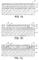
- FIGS. 1A-1I are cross-sectional views of intermediate structures, taken along line 1-1' of FIG. 2, that illustrate preferred methods of forming optoelectronic devices having pop-up mirrors therein, according to a first embodiment of the present invention.
- FIG. 2 is a plan layout schematic of an optoelectronic device having a pop-up mirror therein, according to the first embodiment of the present invention.
- FIG. 3 is a cross-sectional view of the optoelectronic device of FIG. 2, taken along line 3-3'.
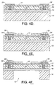
- FIGS. 4A-4I are cross-sectional views of intermediate structures, taken along line 4-4' of FIG. 5, that illustrate preferred methods of forming optoelectronic devices having pop-up mirrors therein, according to a second embodiment of the present invention.
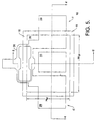
- FIG. 5 is a plan layout schematic of an optoelectronic device having a pop-up mirror therein, according to the second embodiment of the present invention.
- FIG. 6 is a cross-sectional view of the optoelectronic device of FIG. 5, taken along line 6-6'.
- the SOI substrate 10 may comprise a monocrystalline silicon wafer 12 having a thickness of greater than about 100 ⁇ m and an intermediate electrically insulating layer 14 on an upper surface of the silicon wafer 12.
- the intermediate electrically insulating layer 14 may be formed by thermally oxidizing the upper surface of the silicon wafer 12.
- the intermediate electrically insulating layer 14 preferably has a thickness in a range between about 0.1 ⁇ m and 0.5 ⁇ m.
- the SOI substrate 10 also preferably comprises an electrically conductive layer 16 of monocrystalline silicon having a thickness in a range between about 10 ⁇ m and 100 ⁇ m, and more preferably about 50 ⁇ m.
- This electrically conductive layer 16 may have a polished surface and this polished surface may be bonded to the intermediate electrically insulating layer 14 using conventional wafer bonding techniques, for example.
- the electrically conductive layer 16 may be formed on an upper surface of the intermediate electrically insulating layer 14 using epitaxial lateral overgrowth (ELO) techniques.
- ELO epitaxial lateral overgrowth
- a silicon nitride layer 17 having a thickness in a range between about 0.1 and 0.5 ⁇ m may also be formed on the electrically conductive layer 16.
- a mirror backing layer 20 may be defined by forming an endless groove 18 that extends through the electrically conductive layer 16 and exposes the intermediate electrically insulating layer 14 which acts as an etch-stop layer.
- the mirror backing layer 20 may be defined as a rectangular-shaped layer having a width "W M " of about 350 ⁇ m and a height "H M " of about 250 ⁇ m when viewed in an open position.
- the endless groove 18 is preferably formed by selectively etching the electrically conductive layer 16 using a deep reactive ion etching (DRIE) technique that provides a high degree of selectivity and facilitates the formation of a groove 18 having a high aspect ratio.
- DRIE deep reactive ion etching
- This DRIE technique can be performed using a DRIE tool, such as a Multiplex tool manufactured by Surface Technology Systems, Ltd. (see, http://www.stsystems.com/equip.html).
- a groove 18 having a width of 5 ⁇ m and a depth corresponding to the thickness of the electrically conductive layer 16 (e.g, 50 ⁇ m) can be formed.
- the endless groove 18 may at least be partially formed by an anisotropic etching step using a KOH etchant.
- a step is then performed to narrow the effective width of the groove 18.
- This step is preferably achieved by performing a thermal oxidation step to selectively grow oxide spacers 22 on the exposed sidewalls of the electrically conductive layer 16 and the mirror backing layer 20 (using the silicon nitride layer 17 as a thermal oxidation mask).
- the oxide spacers 22 may be formed to have a thickness of about 2 ⁇ m.
- the formation of the oxide spacers 22 will cause the sidewalls of the electrically conductive layer 16 and the mirror backing layer 20 to become recessed since silicon atoms within these layers will be consumed during the thermal oxidation step.
- the oxide spacers may be formed to have a thickness of about 2 ⁇ m for a groove 18 having a width of 5 ⁇ m, the resulting width of the groove 18 after the thermal oxidation step will be greater than about 1 ⁇ m.
- a step is then performed to fill the remaining opening in the groove 18 with an electrically insulating material by depositing a blanket layer of phosphorus-doped silicate glass (PSG) on the structure of FIG. 1C.
- PSG phosphorus-doped silicate glass
- This blanket layer is then planarized to define a sacrificial insulating region 24 within the groove 18.
- the planarization step may comprise a chemical-mechanical polishing (CMP) step.
- CMP chemical-mechanical polishing
- a photolithographically defined etching step may then be performed to remove portions of the blanket silicon nitride layer 17 and thereby expose selected portions of a back surface of the mirror backing layer 20 (contact openings A, B and C) and expose a portion (contact opening D) of the electrically conductive layer 16 that extends adjacent the groove 18.
- a blanket layer of polycrystalline silicon having a thickness in a range between about 1 ⁇ m and 3 ⁇ m (e.g., 2 ⁇ m) is deposited onto the silicon nitride layer 17 and onto the exposed portions of the surface of the electrically conductive layer 16 and back surface of the mirror backing layer 20.
- the blanket layer of polycrystalline silicon is then patterned to define a polysilicon hinge 26 and a pair of polysilicon electrostatic clamp electrodes 28.
- the oxide spacers 22 and sacrificial insulating region 24 within the groove 18 provide support to the blanket layer of polycrystalline silicon during the deposition and patterning steps.
- the polysilicon hinge 26 may be patterned to have a width "W H " of about 8-10 ⁇ m. As illustrated best by FIGS. 2-3, the polysilicon hinge 26 electrically and mechanically couples the mirror backing layer 20 to the electrically conductive layer 16.
- a backside of the monocrystalline silicon wafer 12 is then etched using another deep reactive ion etching (DRIE) technique, to define an opening 19 in the monocrystalline silicon wafer 12 that exposes the intermediate electrically insulating layer 14.
- DRIE deep reactive ion etching
- the intermediate electrically insulating layer 14 acts as an etch-stop layer.
- the size of the opening is preferably designed to be smaller than the size of the mirror backing layer 20 as defined by the groove 18.
- the electrostatic clamping electrodes 28 may also provide a sufficient mechanical support to suspend the mirror backing layer 20 within the opening 19, the size of the opening may be designed to be equal to or larger than the mirror backing layer 20.
- FIGS. 1G and 2 another photolithographically defined etching step is performed on the silicon nitride layer 17, to expose the back surface of the mirror backing layer 20.
- This etching step is then followed by the step of electroplating a layer of nickel 33 having a thickness in a range between about 5 ⁇ m and 30 ⁇ m onto the exposed back surface of the mirror backing layer 20.
- the etching mask that is used during etching of the silicon nitride layer 17 is also used as a mask during the electroplating step.
- a conventional etching step is then performed to remove the exposed portion of the intermediate electrically insulating layer 14 from the front polished surface of the mirror backing layer 20.
- An optically reflective mirror surface 30 is then formed on the front surface of the mirror backing layer 10.
- This mirror surface 30 may be formed by evaporating a layer of gold onto the front surface of the mirror backing layer 20.
- the mirror surface 30 may be formed by evaporating a layer of aluminum onto the front surface of the mirror backing layer 20.
- the mirror surface 30 may also be formed by sputtering a layer of gold or aluminum onto the front surface of the mirror backing layer 20.
- these techniques of evaporating or sputtering gold or aluminum to define the mirror surface 30 result in the formation of a mirror surface 30 that is self-aligned to the opening in the silicon wafer 12.
- the mirror backing layer 20 is then released by performing a selective etching step using the mirror surface 30 and silicon wafer 12 as an etching mask.
- a wet etching step may be performed that causes the intermediate electrically insulating layer 14 to become recessed and removes the oxide spacers 22 and the sacrificial insulating region 24 from within the groove 18, as illustrated by FIG. 1I.
- the mirror backing layer 20 will be supported by the polysilicon electrostatic clamp electrodes 28 and the ledge 12a formed by the silicon wafer 12.
- FIG. 2 a plan layout schematic of an optoelectronic device having a pop-up mirror therein is provided.
- the mirror backing layer 20 is mechanically and electrically coupled to the electrically conductive layer 16 by a polysilicon hinge 26 that enables the mirror backing layer 20 to be rotated from the closed position within the opening to an upright and open position. When in the open position, the mirror backing layer 20 may be disposed orthogonally relative to the electrically conductive layer 16.
- a pair of polysilicon electrostatic clamp electrodes 28 are also provided. These clamp electrodes 28 are attached to the mirror backing layer 20 at contact openings A and B, and are electrically connected to a first portion of the electrically conductive layer 16 (at contact opening D) by the polysilicon hinge 26.
- the clamp electrodes 28 extend opposite regions E and F within the electrically conductive layer 16. Respective portions of the silicon nitride layer 17 also extend between the electrically conductive layer 16 and the ends of each clamp electrode 28. These portions of the silicon nitride layer 17 act as a capacitor dielectric material when an electrostatic potential is established between the underlying portion of the electrically conductive layer 16 and the respective clamp electrode 28. This electrostatic potential induces a downward force F 2 on the clamp electrodes 28.
- a nickel frame layer 33 is also provided on the mirror backing layer 20.
- the application of a magnetic field "B" of sufficient strength through the opening 19 will induce an upward force F 1 on the nickel frame layer 33 that pulls and rotates the mirror backing layer 20 to a substantially upright position.
- This upward force induced by the magnetic field "B” can be countered by the opposite electrostatic force F 2 established between the clamp electrodes 28 and respective opposing regions E and F of the electrically conductive layer 16 (regions E and F are electrically isolated from region G within the electrically conductive layer 16).
- the mirror backing layer 20 may be clamped in a closed position.
- the substrate 10 may comprise a monocrystalline silicon wafer 12 having a thickness of greater than about 100 ⁇ m and an intermediate electrically insulating layer 14 on an upper surface of the silicon wafer 12.
- the intermediate electrically insulating layer 14 may be formed by thermally oxidizing the upper surface of the silicon wafer 12.
- the intermediate electrically insulating layer 14 preferably has a thickness in a range between about 0.1 ⁇ m and 0.5 ⁇ m.
- the substrate 10 also preferably comprises an electrically conductive layer 16 of monocrystalline silicon having a thickness in a range between about 10 ⁇ m and 100 ⁇ m, and more preferably about 50 ⁇ m.
- This electrically conductive layer 16 may have a polished surface and this polished surface may be bonded to the intermediate electrically insulating layer 14 using conventional wafer bonding techniques, for example.
- the electrically conductive layer 16 may be formed on an upper surface of the intermediate electrically insulating layer 14 using epitaxial lateral overgrowth (ELO) techniques.
- ELO epitaxial lateral overgrowth
- a silicon nitride layer 17 having a thickness in a range between about 0.1 and 0.5 ⁇ m may also be formed on the electrically conductive layer 16.
- a mirror backing layer 20 may be defined by forming an endless groove 18 that extends through the electrically conductive layer 16 and exposes the intermediate electrically insulating layer 14 which acts as an etch-stop layer.
- the mirror backing layer 20 may be defined as a rectangular-shaped layer having a width "W M " of about 350 ⁇ m and a height "H M " of about 250 ⁇ m when viewed in an open position.
- the endless groove 18 may be formed by selectively etching the electrically conductive layer 16 using a deep reactive ion etching (DRIE) technique that provides a high degree of selectivity and facilitates the formation of a groove 18 having a high aspect ratio.
- DRIE deep reactive ion etching
- the endless groove 18 may be formed by an anisotropic etching step using a KOH etchant.
- a step is then performed to narrow the effective width of the groove 18.
- This step is preferably achieved by performing a thermal oxidation step to selectively grow oxide spacers 22 on the exposed sidewalls of the electrically conductive layer 16 and the mirror backing layer 20 (using the silicon nitride layer 17 as a thermal oxidation mask).
- the oxide spacers 22 may be formed to have a thickness of about 2 ⁇ m.
- a step is then performed to fill the remaining opening in the groove 18 with an electrically insulating material by depositing a blanket layer of phosphorus-doped silicate glass (PSG) on the structure of FIG. 4C.
- This blanket layer is then patterned to define a sacrificial insulating region 24' within the groove 18 and on the surface of the silicon nitride layer 17, as illustrated.
- a blanket layer of polycrystalline silicon having a thickness in a range between about 1 ⁇ m and 3 ⁇ m (e.g., 2 ⁇ m) is then deposited onto the silicon nitride layer 17 and onto the patterned sacrificial insulating region 24'.
- the blanket layer of polycrystalline silicon is then patterned to define a polysilicon hinge 26 and a pair of polysilicon electrostatic clamp electrodes 28 that are electrically coupled to and contiguous with the hinge 26.
- a backside of the monocrystalline silicon wafer 12 is then etched using a deep reactive ion etching (DRIE) technique, to define an opening 19 in the monocrystalline silicon wafer 12 that exposes the intermediate electrically insulating layer 14.
- DRIE deep reactive ion etching
- the intermediate electrically insulating layer 14 acts as an etch-stop layer.
- a photolithographically defined etching step is performed on the silicon nitride layer 17 to expose the back surface of the mirror backing layer 20.
- This etching step is then followed by the step of electroplating a layer of nickel 33 having a thickness in a range between about 5 ⁇ m and 30 ⁇ m onto the exposed back surface of the mirror backing layer 20.
- the etching mask that is used during etching of the silicon nitride layer 17 is also used as a mask during the electroplating step.
- a conventional etching step is then performed to remove the exposed portion of the intermediate electrically insulating layer 14 from the front polished surface of the mirror backing layer 20.
- An optically reflective mirror surface 30 is then formed on the front surface of the mirror backing layer 10. This mirror surface 30 may be formed by evaporating a layer of gold onto the front surface of the mirror backing layer 20.
- the mirror backing layer 20 is then released by performing a selective etching step using the mirror surface 30 and silicon wafer 12 as an etching mask.
- a wet etching step may be performed that causes the intermediate electrically insulating layer 14 to become recessed and removes the oxide spacers 22 and the sacrificial insulating region 24' from within the groove 18 and underneath the electrostatic clamp electrodes 28, as illustrated by FIG. 4I.
- FIG. 5 a plan layout schematic of an optoelectronic device having a pop-up mirror therein is provided.
- the mirror backing layer 20 is mechanically coupled to the electrically conductive layer 16 by a polysilicon hinge 26 that enables the mirror backing layer 20 to be rotated from the closed position within the opening to an upright and open position. When in the open position, the mirror backing layer 20 may be disposed orthogonally relative to the electrically conductive layer 16.
- a pair of polysilicon electrostatic clamp electrodes 28 are also provided. As illustrated best by FIGS. 4I and 6, the clamp electrodes 28 extend opposite regions E and F within the electrically conductive layer 16.
- Respective portions of the silicon nitride layer 17 also extend between the electrically conductive layer 16 and the ends of each clamp electrode 28. These portions of the silicon nitride layer 17 act as a capacitor dielectric material when an electrostatic potential is established between the underlying portion of the electrically conductive layer 16 and the respective clamp electrode 28. This electrostatic potential induces a downward force F 2 on the clamp electrodes 28.
- a nickel frame layer 33 is also provided on the mirror backing layer 20. As determined by the inventors herein, the application of a magnetic field "B" of sufficient strength through the opening 19 will induce an upward force F 1 on the nickel frame layer 33 that pulls and rotates the mirror backing layer 20 to a substantially upright position.
Landscapes
- Physics & Mathematics (AREA)
- General Physics & Mathematics (AREA)
- Optics & Photonics (AREA)
- Mechanical Light Control Or Optical Switches (AREA)
- Micromachines (AREA)
Abstract
Description
Claims (10)
- A method of forming an optoelectronic device, characterized by the steps of:forming an electrically conductive layer (16) on a first surface of a substrate;forming a mirror backing layer (20) from the electrically conductive layer (16) by forming an endless groove (18) that extends through the electrically conductive layer (16);removing a portion of the substrate at a second surface thereof extending opposite the first surface, to expose a front surface of the mirror backing layer (20); andforming an optically reflective mirror surface (30) on the front surface of the mirror backing layer (20).
- The method of Claim 1, wherein the electrically conductive layer (16) comprises a monocrystalline silicon conductive layer having a thickness of greater than about 10 □m; and wherein said step of forming a mirror backing layer (20) comprises etching an endless groove (18) in the monocrystalline silicon conductive layer using a deep reactive ion etching technique.
- The method of Claim 1, wherein the substrate comprises a supporting layer (12) of monocrystalline silicon having a thickness of greater than about 100 □m; and wherein said step of removing a portion of the substrate comprises etching through the supporting layer (12) of monocrystalline silicon using a deep reactive ion etching technique.
- The method of Claim 2, further characterized by the step of forming a polysilicon hinge (26) that is attached to a back surface of the mirror backing layer (20) and is attached to the electrically conductive layer (16).
- The method of Claim 4, wherein said step of forming a polysilicon hinge (26) comprises forming a polysilicon electrostatic clamping electrode (28) that is attached to the back surface of the mirror backing layer (20) and overlaps the endless groove (18).
- An optoelectronic device, characterized by:a silicon-on-insulator substrate having an opening (19) therein;a mirror (20, 30) that is disposed in the opening when in a closed position; anda polysilicon hinge (26) that mechanically couples said mirror (20, 30) to said silicon-on-insulator substrate so that said mirror (20, 30) can be rotated from the closed position to an open position when a magnetic field is directed to pass through the opening.
- The device of Claim 6, wherein said mirror (20, 30) comprises:a monocrystalline silicon backing layer (20) having a thickness of greater than about 10 □m; andan optically reflective mirror surface (30) on a front surface of said monocrystalline silicon backing layer (20).
- The device of Claim 7, further comprising an electrostatic polysilicon clamp electrode (28) that is attached to the back surface of said monocrystalline silicon backing layer (20).
- The device of Claim 8, wherein said electrostatic polysilicon clamp electrode (28) extends opposite said silicon-on-insulator substrate and provides mechanical support to said mirror (20, 30) when in the closed position.
- A method of operating an optoelectronic device comprising a semiconductor substrate having an opening therein, a mirror (20, 30) disposed in the opening when in a closed position and a hinge (26) that mechanically couples the mirror (20, 30) to the semiconductor substrate, said method characterized by:
applying a magnetic field of sufficient first strength through the opening to cause the mirror (20, 30) to rotate about the hinge (26) from the closed position to an open position.
Applications Claiming Priority (4)
| Application Number | Priority Date | Filing Date | Title |
|---|---|---|---|
| US16531799P | 1999-11-12 | 1999-11-12 | |
| US165317P | 1999-11-12 | ||
| US511928 | 2000-02-23 | ||
| US09/511,928 US6535318B1 (en) | 1999-11-12 | 2000-02-23 | Integrated optoelectronic devices having pop-up mirrors therein and methods of forming and operating same |
Publications (2)
| Publication Number | Publication Date |
|---|---|
| EP1099973A2 true EP1099973A2 (en) | 2001-05-16 |
| EP1099973A3 EP1099973A3 (en) | 2004-07-28 |
Family
ID=26861278
Family Applications (1)
| Application Number | Title | Priority Date | Filing Date |
|---|---|---|---|
| EP00309416A Withdrawn EP1099973A3 (en) | 1999-11-12 | 2000-10-26 | Integrated optoelectronic devices having pop-up mirrors therein and methods of forming and operating same |
Country Status (6)
| Country | Link |
|---|---|
| US (2) | US6535318B1 (en) |
| EP (1) | EP1099973A3 (en) |
| KR (1) | KR20010060300A (en) |
| CN (1) | CN1296191A (en) |
| CA (1) | CA2325096A1 (en) |
| TW (1) | TW488087B (en) |
Cited By (1)
| Publication number | Priority date | Publication date | Assignee | Title |
|---|---|---|---|---|
| KR100464320B1 (en) * | 2002-11-19 | 2004-12-31 | 삼성전자주식회사 | Micromirror actuator and method for manufacturing the same |
Families Citing this family (31)
| Publication number | Priority date | Publication date | Assignee | Title |
|---|---|---|---|---|
| US6506620B1 (en) * | 2000-11-27 | 2003-01-14 | Microscan Systems Incorporated | Process for manufacturing micromechanical and microoptomechanical structures with backside metalization |
| US6695457B2 (en) * | 2001-06-02 | 2004-02-24 | Capella Photonics, Inc. | Bulk silicon mirrors with hinges underneath |
| ATE417021T1 (en) * | 2001-11-09 | 2008-12-15 | Wispry Inc | THREE-LAYER BEAM MEMS DEVICE AND RELATED METHOD |
| US6906846B2 (en) * | 2002-08-14 | 2005-06-14 | Triquint Technology Holding Co. | Micro-electro-mechanical system device and method of making same |
| US6672712B1 (en) * | 2002-10-31 | 2004-01-06 | Hewlett-Packard Development Company, L.P. | Slotted substrates and methods and systems for forming same |
| US7034370B2 (en) * | 2002-11-22 | 2006-04-25 | Advanced Nano Systems, Inc. | MEMS scanning mirror with tunable natural frequency |
| US6769616B2 (en) * | 2002-11-22 | 2004-08-03 | Advanced Nano Systems | Bidirectional MEMS scanning mirror with tunable natural frequency |
| JP4150003B2 (en) * | 2003-04-25 | 2008-09-17 | 富士通株式会社 | Manufacturing method of microstructure and microstructure |
| TW570896B (en) * | 2003-05-26 | 2004-01-11 | Prime View Int Co Ltd | A method for fabricating an interference display cell |
| US7054052B2 (en) * | 2003-09-04 | 2006-05-30 | Frank Niklaus | Adhesive sacrificial bonding of spatial light modulators |
| US6903861B1 (en) | 2004-01-22 | 2005-06-07 | Sandia Corporation | Erected mirror optical switch |
| JP2005250376A (en) * | 2004-03-08 | 2005-09-15 | Seiko Epson Corp | Optical modulator and method for manufacturing optical modulator |
| KR100644896B1 (en) * | 2005-01-19 | 2006-11-14 | 엘지전자 주식회사 | Electromagnetically driven scanning micromirror and optical scanning device using the same |
| KR100703074B1 (en) | 2005-02-25 | 2007-04-06 | 삼성전기주식회사 | Tilting member and tilting actuator having it |
| US7932182B2 (en) * | 2005-08-19 | 2011-04-26 | Honeywell International Inc. | Creating novel structures using deep trenching of oriented silicon substrates |
| US8099247B2 (en) * | 2005-11-23 | 2012-01-17 | Electric Mirror, Llc | Back lit mirror with media display device |
| US20070273954A1 (en) * | 2006-05-24 | 2007-11-29 | Texas Instruments Incorporated | Hinge assembly for a digital micromirror device |
| KR20090125087A (en) * | 2007-02-20 | 2009-12-03 | 퀄컴 엠이엠스 테크놀로지스, 인크. | Etching Apparatus and Etching Method of Microelectromechanical System MEMS |
| KR20100061731A (en) * | 2007-09-14 | 2010-06-08 | 퀄컴 엠이엠스 테크놀로지스, 인크. | Etching processes used in mems production |
| TWI373450B (en) | 2009-07-29 | 2012-10-01 | Pixart Imaging Inc | Microelectronic device and method for fabricating mems resonator thereof |
| US8836100B2 (en) * | 2009-12-01 | 2014-09-16 | Cisco Technology, Inc. | Slotted configuration for optimized placement of micro-components using adhesive bonding |
| US8461656B2 (en) * | 2010-06-30 | 2013-06-11 | Freescale Semiconductor, Inc. | Device structures for in-plane and out-of-plane sensing micro-electro-mechanical systems (MEMS) |
| TWI447365B (en) * | 2011-05-24 | 2014-08-01 | Univ Nat Kaohsiung Applied Sci | Single crystal silicon thermal sensor and its preparation method |
| US9007676B1 (en) * | 2012-09-20 | 2015-04-14 | Copytele, Inc. | MEMS electrostatic display |
| DE102013209238B4 (en) * | 2013-05-17 | 2017-10-12 | Fraunhofer-Gesellschaft zur Förderung der angewandten Forschung e.V. | MEMS structure and method of making same |
| WO2015167521A1 (en) * | 2014-04-30 | 2015-11-05 | Hewlett-Packard Development Company, L.P. | Controllable diamond waveguide tuner |
| US20150355458A1 (en) * | 2014-06-10 | 2015-12-10 | Shuyun (Steve) Wu | Micro-machined optical mirror switch |
| EP3160897A4 (en) * | 2014-06-27 | 2018-01-24 | Intel Corporation | Magnetic nanomechanical devices for stiction compensation |
| US10761312B2 (en) | 2016-09-28 | 2020-09-01 | General Electric Company | Integrated variable view optical adapter for an optical scope |
| DE102018215793A1 (en) * | 2018-09-18 | 2020-03-19 | Robert Bosch Gmbh | Method of manufacturing a semiconductor device and semiconductor device |
| CN111884647B (en) * | 2020-08-13 | 2023-09-29 | 中国工程物理研究院电子工程研究所 | Coupling isolation method for piezoelectric micromechanical acoustic transducer array |
Family Cites Families (26)
| Publication number | Priority date | Publication date | Assignee | Title |
|---|---|---|---|---|
| US5071510A (en) | 1989-09-22 | 1991-12-10 | Robert Bosch Gmbh | Process for anisotropic etching of silicon plates |
| DE4016471A1 (en) | 1990-05-22 | 1991-11-28 | Bosch Gmbh Robert | MICROMECHANICAL INCLINATION SENSOR |
| DE4106933B4 (en) | 1991-03-05 | 2004-12-16 | Robert Bosch Gmbh | patterning methods |
| US5295014A (en) | 1992-11-12 | 1994-03-15 | The Whitaker Corporation | Two-dimensional laser beam scanner using PVDF bimorph |
| ATE269588T1 (en) | 1993-02-04 | 2004-07-15 | Cornell Res Foundation Inc | MICROSTRUCTURES AND SINGLE MASK, SINGLE CRYSTAL PRODUCTION PROCESS |
| US5673139A (en) | 1993-07-19 | 1997-09-30 | Medcom, Inc. | Microelectromechanical television scanning device and method for making the same |
| FR2710161B1 (en) | 1993-09-13 | 1995-11-24 | Suisse Electronique Microtech | Miniature array of light shutters. |
| JP3219123B2 (en) | 1993-11-29 | 2001-10-15 | 株式会社デンソー | Two-dimensional optical scanning device and bar code reader using the same |
| US5579151A (en) * | 1995-02-17 | 1996-11-26 | Texas Instruments Incorporated | Spatial light modulator |
| US5914801A (en) * | 1996-09-27 | 1999-06-22 | Mcnc | Microelectromechanical devices including rotating plates and related methods |
| US5793519A (en) * | 1996-11-15 | 1998-08-11 | Eastman Kodak Company | Micromolded integrated ceramic light reflector |
| US5761350A (en) | 1997-01-22 | 1998-06-02 | Koh; Seungug | Method and apparatus for providing a seamless electrical/optical multi-layer micro-opto-electro-mechanical system assembly |
| US5781331A (en) * | 1997-01-24 | 1998-07-14 | Roxburgh Ltd. | Optical microshutter array |
| US5768009A (en) * | 1997-04-18 | 1998-06-16 | E-Beam | Light valve target comprising electrostatically-repelled micro-mirrors |
| US5880921A (en) | 1997-04-28 | 1999-03-09 | Rockwell Science Center, Llc | Monolithically integrated switched capacitor bank using micro electro mechanical system (MEMS) technology |
| US5903380A (en) | 1997-05-01 | 1999-05-11 | Rockwell International Corp. | Micro-electromechanical (MEM) optical resonator and method |
| US5905007A (en) | 1997-08-01 | 1999-05-18 | The Regents Of The University Of California | Method for aligning and forming microelectromechanical systems (MEMS) contour surfaces |
| US5867302A (en) | 1997-08-07 | 1999-02-02 | Sandia Corporation | Bistable microelectromechanical actuator |
| US6201629B1 (en) * | 1997-08-27 | 2001-03-13 | Microoptical Corporation | Torsional micro-mechanical mirror system |
| US6137623A (en) * | 1998-03-17 | 2000-10-24 | Mcnc | Modulatable reflectors and methods for using same |
| US5910856A (en) * | 1998-04-16 | 1999-06-08 | Eastman Kodak Company | Integrated hybrid silicon-based micro-reflector |
| US5943155A (en) | 1998-08-12 | 1999-08-24 | Lucent Techonolgies Inc. | Mars optical modulators |
| US6014240A (en) * | 1998-12-01 | 2000-01-11 | Xerox Corporation | Method and apparatus for an integrated laser beam scanner using a carrier substrate |
| KR100328710B1 (en) * | 1999-08-23 | 2002-03-20 | 박종섭 | Inductor and fabricating method thereof |
| US6275320B1 (en) * | 1999-09-27 | 2001-08-14 | Jds Uniphase, Inc. | MEMS variable optical attenuator |
| WO2002095800A2 (en) * | 2001-05-22 | 2002-11-28 | Reflectivity, Inc. | A method for making a micromechanical device by removing a sacrificial layer with multiple sequential etchants |
-
2000
- 2000-02-23 US US09/511,928 patent/US6535318B1/en not_active Expired - Lifetime
- 2000-10-26 EP EP00309416A patent/EP1099973A3/en not_active Withdrawn
- 2000-11-03 CA CA002325096A patent/CA2325096A1/en not_active Abandoned
- 2000-11-09 TW TW089123665A patent/TW488087B/en not_active IP Right Cessation
- 2000-11-10 KR KR1020000066795A patent/KR20010060300A/en not_active Withdrawn
- 2000-11-10 CN CN00133799A patent/CN1296191A/en active Pending
-
2002
- 2002-12-02 US US10/307,771 patent/US6942814B2/en not_active Expired - Lifetime
Cited By (1)
| Publication number | Priority date | Publication date | Assignee | Title |
|---|---|---|---|---|
| KR100464320B1 (en) * | 2002-11-19 | 2004-12-31 | 삼성전자주식회사 | Micromirror actuator and method for manufacturing the same |
Also Published As
| Publication number | Publication date |
|---|---|
| US20030117679A1 (en) | 2003-06-26 |
| KR20010060300A (en) | 2001-07-06 |
| EP1099973A3 (en) | 2004-07-28 |
| TW488087B (en) | 2002-05-21 |
| CA2325096A1 (en) | 2001-05-12 |
| CN1296191A (en) | 2001-05-23 |
| US6942814B2 (en) | 2005-09-13 |
| US6535318B1 (en) | 2003-03-18 |
Similar Documents
| Publication | Publication Date | Title |
|---|---|---|
| US6942814B2 (en) | Methods of forming integrated optoelectronic devices | |
| US6528887B2 (en) | Conductive equipotential landing pads formed on the underside of a MEMS device | |
| US6134042A (en) | Reflective mems actuator with a laser | |
| US6753638B2 (en) | Electrostatic actuator for micromechanical systems | |
| US6862127B1 (en) | High performance micromirror arrays and methods of manufacturing the same | |
| JP2987198B2 (en) | Micro mechanical switch | |
| US7445723B2 (en) | Optical scanner and method of fabricating the same | |
| US20020167072A1 (en) | Electrostatically actuated micro-electro-mechanical devices and method of manufacture | |
| JP2001125014A (en) | MEMS device for performing optical attenuation, variable optical attenuation system, optical attenuation method, and method of manufacturing MEMS variable optical attenuator | |
| WO2001056919A2 (en) | Micro-electro-mechanical-system (mems) mirror device and methods for fabricating the same | |
| US6819820B1 (en) | Use of applied force to improve MEMS switch performance | |
| US20060171628A1 (en) | Mems element and method of producing the same, and diffraction type mems element | |
| JP4115116B2 (en) | Thermal microelectrical mechanical actuator | |
| US20050094241A1 (en) | Electromechanical micromirror devices and methods of manufacturing the same | |
| US20020126455A1 (en) | Tiled microelectromechanical device modules and fabrication methods | |
| US20020046985A1 (en) | Process for creating an electrically isolated electrode on a sidewall of a cavity in a base | |
| US20020088224A1 (en) | Resonant thermal out-of-plane buckle-beam actuator | |
| KR100404195B1 (en) | micro mirror and method for fabricating micro mirror | |
| JP3825388B2 (en) | Optical switch device | |
| Kouma et al. | Fishbone-shaped vertical comb actuator for dual-axis 1D analog micromirror array | |
| WO2002084374A1 (en) | Mems mirrors with precision clamping mechanism | |
| KR100396664B1 (en) | micro mirror and method for fabricating micro mirror |
Legal Events
| Date | Code | Title | Description |
|---|---|---|---|
| PUAI | Public reference made under article 153(3) epc to a published international application that has entered the european phase |
Free format text: ORIGINAL CODE: 0009012 |
|
| AK | Designated contracting states |
Kind code of ref document: A2 Designated state(s): AT BE CH CY DE DK ES FI FR GB GR IE IT LI LU MC NL PT SE |
|
| AX | Request for extension of the european patent |
Free format text: AL;LT;LV;MK;RO;SI |
|
| RAP1 | Party data changed (applicant data changed or rights of an application transferred) |
Owner name: JDS UNIPHASE CORPORATION |
|
| RAP1 | Party data changed (applicant data changed or rights of an application transferred) |
Owner name: MEMSCAP S.A. |
|
| RIC1 | Information provided on ipc code assigned before grant |
Ipc: 7B 81B 3/00 B Ipc: 7G 02B 26/08 A |
|
| PUAL | Search report despatched |
Free format text: ORIGINAL CODE: 0009013 |
|
| AK | Designated contracting states |
Kind code of ref document: A3 Designated state(s): AT BE CH CY DE DK ES FI FR GB GR IE IT LI LU MC NL PT SE |
|
| AX | Request for extension of the european patent |
Extension state: AL LT LV MK RO SI |
|
| STAA | Information on the status of an ep patent application or granted ep patent |
Free format text: STATUS: THE APPLICATION IS DEEMED TO BE WITHDRAWN |
|
| 18D | Application deemed to be withdrawn |
Effective date: 20040130 |