EP1098376A2 - Organic EL device and image-reading, data-processing and display apparatus including the device - Google Patents
Organic EL device and image-reading, data-processing and display apparatus including the device Download PDFInfo
- Publication number
- EP1098376A2 EP1098376A2 EP00309881A EP00309881A EP1098376A2 EP 1098376 A2 EP1098376 A2 EP 1098376A2 EP 00309881 A EP00309881 A EP 00309881A EP 00309881 A EP00309881 A EP 00309881A EP 1098376 A2 EP1098376 A2 EP 1098376A2
- Authority
- EP
- European Patent Office
- Prior art keywords
- luminescence
- apertures
- substrate
- electrodes
- layer
- Prior art date
- Legal status (The legal status is an assumption and is not a legal conclusion. Google has not performed a legal analysis and makes no representation as to the accuracy of the status listed.)
- Withdrawn
Links
Images



Classifications
-
- H—ELECTRICITY
- H10—SEMICONDUCTOR DEVICES; ELECTRIC SOLID-STATE DEVICES NOT OTHERWISE PROVIDED FOR
- H10K—ORGANIC ELECTRIC SOLID-STATE DEVICES
- H10K59/00—Integrated devices, or assemblies of multiple devices, comprising at least one organic light-emitting element covered by group H10K50/00
- H10K59/30—Devices specially adapted for multicolour light emission
- H10K59/32—Stacked devices having two or more layers, each emitting at different wavelengths
-
- H—ELECTRICITY
- H10—SEMICONDUCTOR DEVICES; ELECTRIC SOLID-STATE DEVICES NOT OTHERWISE PROVIDED FOR
- H10K—ORGANIC ELECTRIC SOLID-STATE DEVICES
- H10K50/00—Organic light-emitting devices
- H10K50/80—Constructional details
- H10K50/805—Electrodes
-
- H—ELECTRICITY
- H10—SEMICONDUCTOR DEVICES; ELECTRIC SOLID-STATE DEVICES NOT OTHERWISE PROVIDED FOR
- H10K—ORGANIC ELECTRIC SOLID-STATE DEVICES
- H10K59/00—Integrated devices, or assemblies of multiple devices, comprising at least one organic light-emitting element covered by group H10K50/00
- H10K59/80—Constructional details
- H10K59/805—Electrodes
-
- H—ELECTRICITY
- H10—SEMICONDUCTOR DEVICES; ELECTRIC SOLID-STATE DEVICES NOT OTHERWISE PROVIDED FOR
- H10K—ORGANIC ELECTRIC SOLID-STATE DEVICES
- H10K85/00—Organic materials used in the body or electrodes of devices covered by this subclass
- H10K85/30—Coordination compounds
- H10K85/321—Metal complexes comprising a group IIIA element, e.g. Tris (8-hydroxyquinoline) gallium [Gaq3]
- H10K85/324—Metal complexes comprising a group IIIA element, e.g. Tris (8-hydroxyquinoline) gallium [Gaq3] comprising aluminium, e.g. Alq3
-
- H—ELECTRICITY
- H10—SEMICONDUCTOR DEVICES; ELECTRIC SOLID-STATE DEVICES NOT OTHERWISE PROVIDED FOR
- H10K—ORGANIC ELECTRIC SOLID-STATE DEVICES
- H10K85/00—Organic materials used in the body or electrodes of devices covered by this subclass
- H10K85/60—Organic compounds having low molecular weight
-
- H—ELECTRICITY
- H10—SEMICONDUCTOR DEVICES; ELECTRIC SOLID-STATE DEVICES NOT OTHERWISE PROVIDED FOR
- H10K—ORGANIC ELECTRIC SOLID-STATE DEVICES
- H10K85/00—Organic materials used in the body or electrodes of devices covered by this subclass
- H10K85/60—Organic compounds having low molecular weight
- H10K85/631—Amine compounds having at least two aryl rest on at least one amine-nitrogen atom, e.g. triphenylamine
Definitions
- the present invention relates to an (electro-)luminescence device utilized in copying machines, printers and display apparatus, e.g., as a backlight device for a display apparatus and a light source for illuminating an original in an image-reading apparatus.
- an (electro-)luminescence device utilized in copying machines, printers and display apparatus, e.g., as a backlight device for a display apparatus and a light source for illuminating an original in an image-reading apparatus.
- tubes and bulbs such as incandescent lamps utilizing light emission caused by resistance heating and fluorescent tubes utilizing light emission caused by discharge in dilute gas
- semiconductor devices such as light-emitting diodes (LED) utilizing light-emission caused by recombination of electrons and holes at pn-junctions formed in organic crystals.
- LED light-emitting diodes
- the tubes and bulbs have been most frequently used, but LEDs have been frequently used as indicators for various electronic appliances.
- liquid crystal display apparatus equipped with fluorescent lamps as a backlight have been used as a display device for computers and portable display terminals.
- functional devices such as light sources for illuminating originals in image reading apparatus for facsimile apparatus and image scanners, and photo-writing heads in LED printers.
- the tubes and bulbs are suitable for emitting intense light by receiving a large electric power but are large in size and liable to be broken. Further, they are not suitable for usages requiring a high-speed responsiveness.
- LEDs can emit only relatively weak light but are advantageous in that they are small in size, have excellent reliability and have high-speed responsiveness.
- an electroluminescence device wherein a thin film layer comprising a crystalline fluorescent substance is formed on a substrate by coating or vapor deposition and is supplied with an AC electric field via an insulating layer to cause luminescence.
- Such an electroluminescence device can be formed in a thin film on a substrate and is advantageous for usages for uniformly illuminating wide ranges or for providing a small-sized, particularly a thin, apparatus including a light source.
- an organic film luminescence device also called an organic LED device
- an organic film luminescence device which is provided in a film on a substrate, provides high luminance and allows a DC drive.
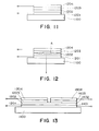
- Figure 11 illustrates a representative organization (laminar structure) of such an organic LED device.
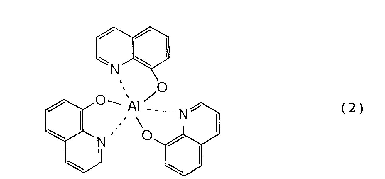
- an organic LED device includes a substrate 1100, an anode 1201 comprising a transparent electrode of indium tin oxide (ITO), a hole-transporting layer 1202 comprising an organic hole-transporting material, such as an organic diamine (of, e.g., formula (1) below), an electron-transporting layer 1203 comprising an organic electron-transporting material, such as tris(8-quinolinolato)aluminum (of formula (2) below) and a cathode 1204 of a substance having a low work function such as Al and/or Hg-Ag alloy, laminated in this order.
- ITO indium tin oxide
- hole-transporting layer 1202 comprising an organic hole-transporting material, such as an organic diamine (of, e.g., formula (1) below)
- an electron-transporting layer 1203 comprising an organic electron-transporting material, such as tris(8-quinolinolato)aluminum (of formula (2) below)
- Figure 12 illustrates a state of luminescence occurring in the organic LED device of Figure 11.
- a portion denoted by A schematically represents the luminescence caused by recombination of holes injected to the hole-transporting layer 1202 from the anode 1201 and electrons injected to the electron-transporting layer 1203 from the cathode 1204.
- Such organic LED devices can emit various colors of luminescence, e.g., by using different organic materials for the hole-transporting layer 1202 or the electron-transporting layer 1203, by admixing another organic material into these layers, or by inserting a luminescence layer comprising another organic material between these layers.
- the luminescence color is determined by organic materials constituting a luminescence part, so that pixels of respectively different luminescence colors have to be formed in a usage, like a full-color display, requiring independent control of different luminescence colors.
- Figure 13 illustrates a typical organization of such an organic LED device.
- the organic LED device includes a substrate 1100; a first pixel comprising an anode (portion) 1201 comprising ITO for the first pixel, a hole-transporting layer (portion) 1202 of an aromatic diamine (of formula (1)), an electron-transporting layer/luminescence layer 1203 of tris(8-quinolinolato)aluminum (of formula (2)) and a cathode 1204 of Al or Hg-Ag alloy, etc.; and also a second pixel comprising an anode (portion) 1401 comprising ITO, a hole-transporting layer (portion) 1202 of an aromatic diamine (of formula (1)), an electron-transporting layer/luminescence layer 1203 of a mixture of tris(8-quinolinolato)aluminum complex (of formula (2)) and a fluorescent substance (of formula (3) below), and a cathode 1404 of Al or Mg-Ag alloy.
- the first pixel emits green luminescence
- the second pixel emits red luminescence
- the respective luminescence layers 1203, 1403 and the respective cathodes 1204, 1404 have to be patterned into shapes of the respective pixels. Moreover, if the cathodes 1204 and 1404 of the adjacent pixels directly contact each other, or even in a single pixel, if the cathode 1204 (1404) directly contacts the anode 1202 (1401) or the hole-transporting layer 1202 (1402), phenomena, such as crosstalk and current leakage, undesirable for the device performances, are liable to occur, so that the mutually adjacent pixels have to be formed in sufficient separation from each other.
- the directively of illumination light reaching a certain point on the original can be different for respective luminescence colors due to the fact that different luminescence colors are emitted from fairly separated different pixels, so that color irregularity is liable to occur depending on the surface gloss of the original.
- a principal object of the present invention is to provide a luminescence device, particularly an organic LED device, having a minimized difference in sites for emitting different luminescence colors.
- a luminescence device comprising a substrate, and a laminated layer structure formed on the substrate including a plurality of luminescence layers emitting different luminescence colors, and a plurality of electrodes forming at least one pair of electrodes each sandwiching an associated luminescence layer, wherein at least one of the plurality of electrodes is provided with apertures, through which a luminescence flux emitted from at least one of the luminescence layers is caused to pass.
- Each of the plurality of luminescence layers may comprise one or more organic compound layers.
- plural layers of electrodes each belonging to different pairs of electrodes sandwiching associated luminescence layers of different luminescence colors are respectively provided with apertures of which positions and/or sizes may be at least partially different from each other.
- each pair of electrodes sandwiching an associated luminescence layer may comprise one transparent electrode on a side closer to the substrate and the other opaque electrode provided with apertures on a side remoter from the substrate, so that the luminescence flux is emitted through the substrate.
- At least one luminescence layer may be sandwiched by a pair of electrodes which are both provided with apertures of which positions and/or sizes are at least partially different from each other so that the pair of electrodes comprises one transparent electrode on a side closer to the substrate and the other opaque electrode, and luminescence light flux is emitted in a direction leaving away from the substrate.
- the present invention further provides an image-reading apparatus including a luminescence device as described above as an illumination light source, and a data processing apparatus including such an image-reading apparatus as a data-reading unit.
- the present invention further provides a display apparatus including a luminescence device as described above as a display unit.
- Figures 1, 3 and 5 are schematic sectional views showing organization of organic LED devices according to a first, a second and a third embodiment, respectively, of the invention.
- Figures 2, 4 and 6 are schematic sectional views illustrating luminescence states in the organic LED devices of Figures 1, 3 and 5, respectively.
- Figures 7 is a partial perspective of an image-reading apparatus including an organic LED device of the second embodiment ( Figure 3) as a light source for illuminating an original.
- Figure 8 is a plan view of the organic LED device of Figure 7 as viewed from the glass substrate side thereof.
- Figure 9 is an enlarged view of a part D shown in Figure 8.
- Figure 10 is an illustration of a facsimile apparatus including the image-reading apparatus of Figure 7.
- Figure 11 is a schematic sectional view showing a typical organization of a conventional organic LED device.
- Figure 12 is a schematic sectional view illustrating a luminescence state in the organic LED device of Figure 11.
- Figure 13 is a schematic sectional view showing a typical organization of a conventional organic LED including separate pixels of mutually different luminescence colors.
- Figure 1 illustrates a laminar organization of an organic LED device according to a first embodiment of the present invention.
- the organic LED device includes a substrate 100;
- Figure 2 schematically illustrates a state of luminescence occurring in the organic LED device of Figure 1.
- each portion A represents luminescence caused by recombination of holes injected to the hole-transporting layer 202 from the first anode 201 and electrons injected to the electron-transporting layer 203 from the first anode 204.
- green luminescence inherent to tris(8-quinolinolato)aluminum complex of formula (2) constituting the electron-transporting layer/luminescence layer 203 is emitted.
- the first cathode 204 is provided with the apertures 205 so that the luminescence is not caused at parts corresponding to the apertures 205.
- each portion B represents luminescence caused by recombination of holes injected to the hole-transporting layer 402 from the second anode 401 and electrons injected to the electron-transporting layer 403 from the second anode 404.
- red luminescence attributable to the fluorescent substance (of formula (3)) added thereto as a dopant is predominant.
- the second cathode 404 is provided with the apertures 405 so that the luminescence is not caused at parts corresponding to the apertures 405.
- the red luminescence flux occurring at the portion B is transmitted through the apertures 205 formed in the first cathode 204 and emitted together with the green luminescence flux occurring at the portions A through the substrate 100.
- pixels of different luminescence colors need not be formed at (horizontally) different positions, but different luminescence colors can be emitted from a horizontally single pixel.
- the sizes of the apertures 205 and 405 it is possible to provide an organic LED device from which different luminescence colors can be emitted from luminescence positions which are substantially free from local deviation (with a minimized positional deviation) relative to a pixel size.
- the green luminescence is caused by a voltage applied between the first anode 201 and the first cathode 204
- the red luminescence is caused by a voltage applied between the second anode 401 and the second cathode 404, so that the respective luminescence colors can be independently emitted, thus allowing at least three color luminescences of green, red and orange (as mixture of green and red) to be issued from a substantially single pixel.
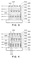
- Figure 3 illustrated a laminar organization of an organic LED device according to a second embodiment of the present invention.
- the organic LED device includes a substrate 100;
- Figure 4 schematically illustrates a state of luminescence occurring in the organic LED device of Figure 3.
- each portion A represents luminescence caused by recombination of holes injected to the hole-transporting layer 202 from the first anode 201 and electrons injected to the electron-transporting layer 203 from the first anode 204.
- green luminescence inherent to tris(8-quinolinolato)aluminum complex of formula (2)) constituting the electron-transporting layer/luminescence layer 203 is emitted.
- the first cathode 204 is provided with the apertures 205 so that the luminescence is not caused at parts corresponding to the apertures 205.
- each portion B represents luminescence caused by recombination of holes injected to the hole-transporting layer 402 from the second anode 401 and electrons injected to the electron-transporting layer 403 from the second anode 404.
- red luminescence attributable to the fluorescent substance (of formula (3)) added thereto as a dopant is predominant.
- the second cathode 404 is provided with the apertures 405 so that the luminescence is not caused at parts corresponding to the apertures 405.
- each portion C represents luminescence caused by recombination of holes injected to the hole-transporting layer 602 from the third anode 601 and electrons injected to the electron-transporting layer 603 from the third anode 604.
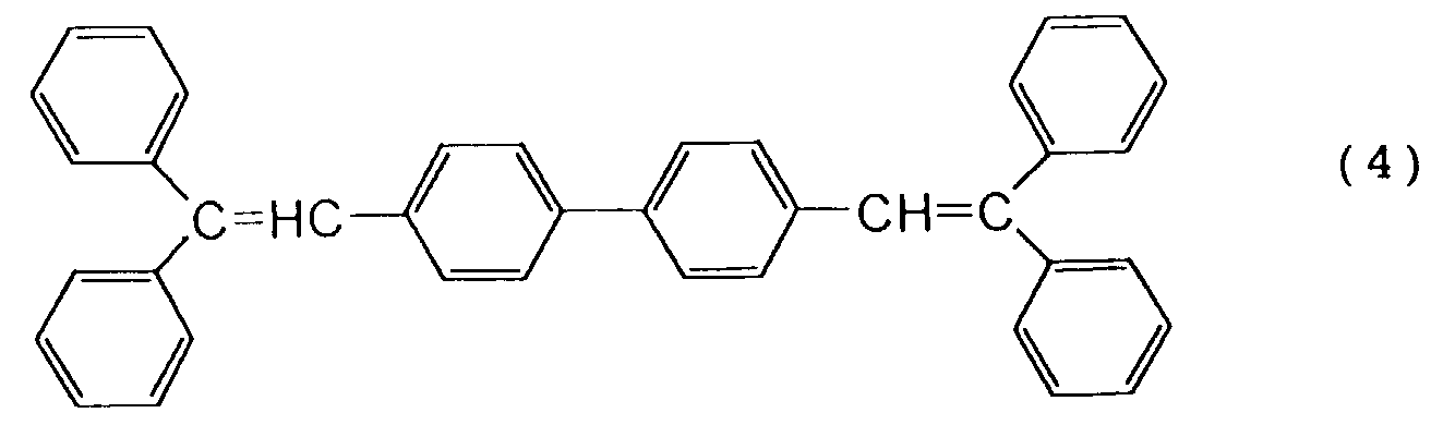
- blue luminescence attributable to the distyryl derivative (of formula (4)) added to tris(8-quinolinolato)aluminum complex as a dopant is predominant.
- the third cathode 604 is provided with the apertures 605 so that the luminescence is not caused at parts corresponding to the apertures 605.
- the red and blue luminescence fluxes occurring at the portion B and C are transmitted through the apertures 205 formed in the first cathode 204 and emitted together with the green luminescence flux occurring at the portions A through the substrate 100.
- the different luminescence colors of R, G and B can be emitted from a horizontally single pixel.
- the sizes of the apertures 205, 405 and 605 it is possible to provide an organic LED device from which different luminescence colors can be emitted with substantially no local deviation relative to a pixel size.
- the green luminescence is caused by a voltage applied between the first anode 201 and the first cathode 204
- the red luminescence is caused by a voltage applied between the second anode 401 and the second cathode 404
- the blue color is caused by a voltage applied between the third mode 601 and the third cathode 604, so that the respective luminescence colors can be independently emitted.
- Figure 5 illustrates a laminar organization of an organic LED device according to a third embodiment of the present invention.
- the organic LED device includes a substrate 100;
- Figure 6 schematically illustrates a state of luminescence occurring in the organic LED device of Figure 5.
- each portion A represents luminescence caused by recombination of holes injected to the hole-transporting layer 202 from the first anode 201 and electrons injected to the electron-transporting layer 203 from the first anode 204.
- green luminescence inherent to tris(8-quinolinolato)aluminum complex of formula (2)) constituting the electron-transporting layer/luminescence layer 203 is emitted.
- the first anode 201 is provided with apertures 206
- the first cathode 204 is provided with apertures 205
- the apertures 206 and 205 are formed at mutually slightly deviated positions, so that the luminescence occurs at positions corresponding to edges of the apertures 205 and 206.
- each portion B represents luminescence caused by recombination of holes injected to the hole-transporting layer 402 from the second anode 401 and electrons injected to the electron-transporting layer 403 from the second anode 404.
- green luminescence inherent to tris(8-quinolinolato)aluminum complex constituting the electron-transporting layer/luminescence layer 403
- red luminescence attributable to the fluorescent substance (of formula (3)) added thereto as a dopant is predominant.
- the second anode 401 is provided with apertures 406, the second cathode 404 is provided with apertures 405, and the apertures 406 and 405 are formed at mutually slightly deviated positions, so that the luminescence occurs at positions corresponding to edges of the apertures 405 and 406.
- each portion C represents luminescence caused by recombination of holes injected to the hole-transporting layer 602 from the third anode 601 and electrons injected to the electron-transporting layer 603 from the third anode 604.
- blue luminescence attributable to the distyryl derivative (of formula (4)) added to tris(8-quinolinolato)aluminum complex as a dopant is predominant.
- the third anode 601 is provided with apertures 606, the third cathode 604 is provided with apertures 605, and the apertures 606 and 605 are formed at mutually slightly deviated positions, so that the luminescence occurs at positions corresponding to edges of the apertures 605 and 606.
- the portions A, B and C causing luminescence are disposed at edges of the apertures, so that the respectively generated luminescence fluxes at A, B and C are emitted through the apertures 205 of the first cathode 204, the apertures 405 of the second 404 and the apertures 605 of the third cathode 604 to be emitted to a side opposite to the substrate 100.
- the different luminescence colors of R, G and B can be emitted from a horizontally single pixel.
- the sizes of the apertures 205, 405 and 605 it is possible to provide an organic LED device from which different luminescence colors can be emitted with substantially no local deviation relative to a pixel size.
- the green luminescence is caused by a voltage applied between the first anode 201 and the first cathode 204
- the red luminescence is caused by a voltage applied between the second anode 401 and the second cathode 404
- the blue color is caused by a voltage applied between the third mode 601 and the third cathode 604, so that the respective luminescence colors can be independently emitted.
- Figure 7 illustrates a part of an image-reading apparatus 8 adopting the organic LED device shown in Figure 3 according to the second embodiment of the present invention as a light source for illuminating an original.
- the image-reading apparatus 8 includes an organic LED device 1 as described above, a rod lens array 2, a photoconverter element array 3, a circuit substrate 4, a housing 5 and a glass sheet 6 supporting an original 7.
- Light flux emitted from the organic LED device 1 supported in the housing 5 is transmitted through the glass sheet 6 to illuminate a surface of the original 7 supported thereon.
- Light flux reflected at the original 7 is passed through the rod lens array 2 to be focused at the photoconverter element array 3 mounted on the circuit substrate 4.
- image data on the original 7 surface is read out by conversion into electric signals.
- the image reading apparatus 8 thus comprising the organic LED device 1, the rod lens array 2, the photoelectric converter element array 3, the circuit substrate 4 and the housing 5 is disposed to extend in a direction parallel to a side of the original supporting glass sheet 6 and is moved in an indicated arrow direction perpendicular to the extension direction thereof, so that images are read in a rectangular region determined by the length and the movement distance of the image reader 8.
- Figure 8 shows a plan view of the organic LED device 1 in Figure 7 as viewed from the side of the glass sheet 6 in Figure 7.
- the organic LED device (1) includes a transparent substrate 100 of, e.g., glass or plastic sheet, a light-emitting unit 101 as observed through the transparent substrate 100 and a flexible circuit sheet 102.
- the anode, the cathode and the organic layer constituting the light-emitting unit 101 are disposed on a back of the substrate 100.
- Figure 9 is an enlarged view of a section D shown in Figure 8 showing the organization of the light-emitting unit 101 as observed through the transparent substrate 100. More specifically, regarding the organization of the light-emitting unit (101 in Figure 8) formed on the transparent substrate 100, Figure 9 shows a first anode 201 (of the organic LED device shown in Figure 3) comprising a transparent electrode of ITO, a first cathode 204 comprising a conductor having a low work function such as Al or Mg-Ag alloy provided with apertures 205, a second cathode 404, and a third cathode 604. The respective electrodes are connected to the flexible circuit sheet 102.
- a first anode 201 of the organic LED device shown in Figure 3
- a first cathode 204 comprising a conductor having a low work function such as Al or Mg-Ag alloy provided with apertures 205
- a second cathode 404 and a third cathode 604.
- the respective electrodes are connected
- Luminescence emitted from the third and second luminescence layers (603 and 403 in Figure 3) are transmitted through the apertures 205 and emitted for illuminating the original surface together with the luminescence emitted from the first luminescence layer (203 in Figure 3).
- the positions of luminescence of different colors are substantially free from positional deviation, so that the directionality of illumination light reaching a certain point on the original is not different depending on different luminescence colors, so that the liability of color irregularity due to surface gloss of the original is deviated, thus allowing high-quality reading.
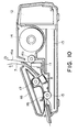
- Figure 10 is a side sectional view of a facsimile apparatus as a data processing apparatus including the image-reading apparatus of Figure 7, which allows high-quality data processing through high-quality image reading owing to the use of an image-reading apparatus according to the present invention.
- the facsimile apparatus incudes an image-reading apparatus 8, a recording head 11, a power supply unit 12, a system control board 13, a recording medium roll 14 from which a recording medium 14a is supplied via a platen roller 14b so as to allow recording by the recording head 11, a feed roller 15 for feeding an original 7 via a separation claw 16 and a platen roller 17, and an operation panel 18.
- the image reading apparatus is applicable not only to such a facsimile apparatus but also to various data processing apparatus, such as a scanner apparatus, utilizing a function of converting optical data into electric signals.
- the organic LED device according to the present invention can also be used to constitute a (color) display apparatus allowing a high-quality display free from recognition of color points.
Landscapes
- Physics & Mathematics (AREA)
- Optics & Photonics (AREA)
- Electroluminescent Light Sources (AREA)
- Facsimile Scanning Arrangements (AREA)
- Devices For Indicating Variable Information By Combining Individual Elements (AREA)
- Led Devices (AREA)
- Printers Or Recording Devices Using Electromagnetic And Radiation Means (AREA)
Abstract
Description


(Respective layer thickness)
- Pixel: 300 µm x 300 µm
- Aperture (205, 405): 50 µm x 300 µm
10 volts between each pair of an anode and a cathode.
Claims (9)
- A luminescence device, comprising a substrate, and a laminated layer structure formed on the substrate including a plurality of luminescence layers emitting different luminescence colors, and a plurality of electrodes forming at least one pair of electrodes each sandwiching an associated luminescence layer, wherein at least one of the plurality of electrodes are provided with apertures, through which a luminescence flux emitted from at least one of the luminescence layers is caused to pass.
- A luminescence device according to Claim 1, wherein each luminescence layer comprises at least one organic compound layer.
- A luminescence device according to Claim 1, wherein plural layers of electrodes each belonging to different pairs of electrodes sandwiching associated luminescence layers of different luminescence colors are respectively provided with apertures of which positions and/or sizes are at least partially different from each other.
- A luminescence device according to Claim 3, wherein each pair of electrodes sandwiching an associated luminescence layer comprises one transparent electrode on a side closer to the substrate and the other opaque electrode provided with apertures on a side remoter from the substrate, and the luminescence flux is emitted through the substrate.
- A luminescence device according to Claim 1, wherein at least one luminescence layer is sandwiched by a pair of electrodes which are both provided with apertures of which positions and/or sizes are at least partially different from each other.
- A luminescence device according to Claim 5, wherein said pair of electrodes comprises one transparent electrode on a side closer to the substrate and the other opaque electrode, and luminescence light flux is emitted in a direction leaving away from the substrate.
- An image-reading apparatus, including a luminescence device according to any one of Claims 1 - 6 as an illumination light source.
- A data processing apparatus including an image-reading apparatus according to Claim 7 as an image-reading unit.
- A display apparatus, including a luminescence device according to any one of Claims 1 - 6 as a display unit.
Applications Claiming Priority (2)
| Application Number | Priority Date | Filing Date | Title |
|---|---|---|---|
| JP31668399A JP2001135479A (en) | 1999-11-08 | 1999-11-08 | Light emitting device, and image reading device, information processing device and display device using the same |
| JP31668399 | 1999-11-08 |
Publications (2)
| Publication Number | Publication Date |
|---|---|
| EP1098376A2 true EP1098376A2 (en) | 2001-05-09 |
| EP1098376A3 EP1098376A3 (en) | 2004-05-19 |
Family
ID=18079754
Family Applications (1)
| Application Number | Title | Priority Date | Filing Date |
|---|---|---|---|
| EP00309881A Withdrawn EP1098376A3 (en) | 1999-11-08 | 2000-11-07 | Organic EL device and image-reading, data-processing and display apparatus including the device |
Country Status (3)
| Country | Link |
|---|---|
| US (1) | US6566806B1 (en) |
| EP (1) | EP1098376A3 (en) |
| JP (1) | JP2001135479A (en) |
Cited By (7)
| Publication number | Priority date | Publication date | Assignee | Title |
|---|---|---|---|---|
| GB2400979A (en) * | 2003-04-24 | 2004-10-27 | Fuji Electric Holdings Co | Organic white light emitting device comprising two or more electroluminescent layers |
| WO2004055897A3 (en) * | 2002-12-18 | 2004-12-16 | Matsushita Electric Industrial Co Ltd | Exposing apparatus and image forming apparatus using organic electroluminescence element |
| WO2005006460A1 (en) * | 2003-07-09 | 2005-01-20 | Matsushita Electric Industrial Co., Ltd. | Organic electroluminescence element and an exposure unit and image-forming apparatus both using the element |
| WO2006006975A1 (en) | 2004-06-18 | 2006-01-19 | General Electric Company | Stacked organic electroluminescent devices |
| EP1441545A3 (en) * | 2003-01-24 | 2006-05-17 | Pioneer Corporation | Stereoscopic image display device |
| US7158161B2 (en) | 2002-09-20 | 2007-01-02 | Matsushita Electric Industrial Co., Ltd. | Organic electroluminescence element and an exposure unit and image-forming apparatus both using the element |
| WO2008070372A1 (en) * | 2006-12-06 | 2008-06-12 | General Electric Company | Color tunable oled illumination display and method for controlled display illumination |
Families Citing this family (27)
| Publication number | Priority date | Publication date | Assignee | Title |
|---|---|---|---|---|
| US6623870B1 (en) * | 1996-08-02 | 2003-09-23 | The Ohio State University | Electroluminescence in light emitting polymers featuring deaggregated polymers |
| JP4593019B2 (en) * | 2001-06-25 | 2010-12-08 | 株式会社半導体エネルギー研究所 | Method for manufacturing light emitting device |
| WO2003013192A1 (en) * | 2001-07-27 | 2003-02-13 | The Ohio State University | Methods for fabricating polymer light emitting devices by lamination |
| JP4865165B2 (en) * | 2001-08-29 | 2012-02-01 | 株式会社半導体エネルギー研究所 | Method for manufacturing light emitting device |
| JP3933915B2 (en) * | 2001-11-09 | 2007-06-20 | セイコーインスツル株式会社 | Illumination device with reflection layer and liquid crystal display device |
| US20030181826A1 (en) * | 2001-12-04 | 2003-09-25 | Dave Smith | Hydrophobic/hydrophilic sample collection tip |
| SG142163A1 (en) | 2001-12-05 | 2008-05-28 | Semiconductor Energy Lab | Organic semiconductor element |
| JP4060113B2 (en) * | 2002-04-05 | 2008-03-12 | 株式会社半導体エネルギー研究所 | Light emitting device |
| JP2003332560A (en) * | 2002-05-13 | 2003-11-21 | Semiconductor Energy Lab Co Ltd | Semiconductor device and microprocessor |
| EP1367659B1 (en) * | 2002-05-21 | 2012-09-05 | Semiconductor Energy Laboratory Co., Ltd. | Organic field effect transistor |
| CN1742518B (en) | 2003-01-29 | 2010-09-29 | 株式会社半导体能源研究所 | light emitting device |
| KR20060126460A (en) * | 2003-11-03 | 2006-12-07 | 바이엘(스위스) 아게 | Electroluminescent systems |
| DE602004021430D1 (en) * | 2004-02-09 | 2009-07-16 | Toyota Ind Corp | TRANSLECTIVE DISPLAY WITH A COLOR OLED BACKLIGHT |
| JP4595565B2 (en) * | 2005-01-31 | 2010-12-08 | 株式会社デンソー | Self-luminous display device |
| KR101097301B1 (en) * | 2005-02-05 | 2011-12-23 | 삼성모바일디스플레이주식회사 | White light emitting device |
| US20060244371A1 (en) * | 2005-05-02 | 2006-11-02 | Eastman Kodak Company | OLED device having improved lifetime and output |
| EP1784055A3 (en) * | 2005-10-17 | 2009-08-05 | Semiconductor Energy Laboratory Co., Ltd. | Lighting system |
| US8680693B2 (en) * | 2006-01-18 | 2014-03-25 | Lg Chem. Ltd. | OLED having stacked organic light-emitting units |
| US7667383B2 (en) * | 2006-02-15 | 2010-02-23 | Osram Opto Semiconductors Gmbh | Light source comprising a common substrate, a first led device and a second led device |
| US20090284158A1 (en) * | 2008-05-16 | 2009-11-19 | General Electric Company | Organic light emitting device based lighting for low cost, flexible large area signage |
| JP2010034035A (en) * | 2008-06-27 | 2010-02-12 | Canon Inc | Organic el display device and method of manufacturing the same |
| US8022623B2 (en) * | 2008-08-15 | 2011-09-20 | General Electric Company | Ultra-thin multi-substrate color tunable OLED device |
| EP2384228A4 (en) * | 2009-01-05 | 2012-06-13 | Plextronics Inc | ILLUMINATION SYSTEM FOR PHOTOTHERAPY WITH ORGANIC LIGHT EMITTING DIODES |
| US20110248244A1 (en) * | 2009-10-05 | 2011-10-13 | Emagin Corporation | Independently controlled stacked inverted organic light emitting diodes and a method of manufacturing same |
| WO2016132460A1 (en) * | 2015-02-17 | 2016-08-25 | パイオニア株式会社 | Light-emitting device |
| US11362133B2 (en) * | 2019-09-11 | 2022-06-14 | Jade Bird Display (shanghai) Limited | Multi-color LED pixel unit and micro-LED display panel |
| CN110957347A (en) * | 2019-12-13 | 2020-04-03 | 苏州星烁纳米科技有限公司 | Light-emitting structure, display device and lighting device |
Family Cites Families (8)
| Publication number | Priority date | Publication date | Assignee | Title |
|---|---|---|---|---|
| JP2823156B2 (en) | 1985-07-23 | 1998-11-11 | キヤノン株式会社 | Display device |
| JPH07114350A (en) * | 1993-10-14 | 1995-05-02 | Pioneer Electron Corp | Electroluminescence display device |
| US5707745A (en) * | 1994-12-13 | 1998-01-13 | The Trustees Of Princeton University | Multicolor organic light emitting devices |
| GB9507862D0 (en) * | 1995-04-18 | 1995-05-31 | Cambridge Display Tech Ltd | Fabrication of organic light-emitting devices |
| JPH1012380A (en) * | 1996-06-25 | 1998-01-16 | Idemitsu Kosan Co Ltd | Multicolor light emitting device and method of manufacturing the same |
| DE69729394T2 (en) * | 1996-11-29 | 2005-06-02 | Idemitsu Kosan Co. Ltd. | Organic electroluminescent device |
| US5917280A (en) * | 1997-02-03 | 1999-06-29 | The Trustees Of Princeton University | Stacked organic light emitting devices |
| JP4267136B2 (en) * | 1998-09-25 | 2009-05-27 | 富士フイルム株式会社 | Radiation image detection and reading device |
-
1999
- 1999-11-08 JP JP31668399A patent/JP2001135479A/en not_active Withdrawn
-
2000
- 2000-11-02 US US09/703,811 patent/US6566806B1/en not_active Expired - Fee Related
- 2000-11-07 EP EP00309881A patent/EP1098376A3/en not_active Withdrawn
Cited By (10)
| Publication number | Priority date | Publication date | Assignee | Title |
|---|---|---|---|---|
| US7158161B2 (en) | 2002-09-20 | 2007-01-02 | Matsushita Electric Industrial Co., Ltd. | Organic electroluminescence element and an exposure unit and image-forming apparatus both using the element |
| WO2004055897A3 (en) * | 2002-12-18 | 2004-12-16 | Matsushita Electric Industrial Co Ltd | Exposing apparatus and image forming apparatus using organic electroluminescence element |
| EP1441545A3 (en) * | 2003-01-24 | 2006-05-17 | Pioneer Corporation | Stereoscopic image display device |
| US7355563B2 (en) | 2003-01-24 | 2008-04-08 | Pioneer Corporation | Display apparatus and display device |
| GB2400979A (en) * | 2003-04-24 | 2004-10-27 | Fuji Electric Holdings Co | Organic white light emitting device comprising two or more electroluminescent layers |
| GB2400979B (en) * | 2003-04-24 | 2006-04-26 | Fuji Electric Holdings Co | Organic light-emitting device |
| WO2005006460A1 (en) * | 2003-07-09 | 2005-01-20 | Matsushita Electric Industrial Co., Ltd. | Organic electroluminescence element and an exposure unit and image-forming apparatus both using the element |
| WO2006006975A1 (en) | 2004-06-18 | 2006-01-19 | General Electric Company | Stacked organic electroluminescent devices |
| WO2008070372A1 (en) * | 2006-12-06 | 2008-06-12 | General Electric Company | Color tunable oled illumination display and method for controlled display illumination |
| CN101601079B (en) * | 2006-12-06 | 2013-07-03 | 通用电气公司 | Color-tunable OLED lighting display device and method for controllable display lighting |
Also Published As
| Publication number | Publication date |
|---|---|
| US6566806B1 (en) | 2003-05-20 |
| JP2001135479A (en) | 2001-05-18 |
| EP1098376A3 (en) | 2004-05-19 |
Similar Documents
| Publication | Publication Date | Title |
|---|---|---|
| US6566806B1 (en) | Luminescence device, and image-reading apparatus, data-processing apparatus and display apparatus including the device | |
| US12009385B2 (en) | Light-emitting diode unit for display comprising plurality of pixels and display device having same | |
| US12490565B2 (en) | Multi-LED structures with single current and voltage supplies | |
| KR100719827B1 (en) | Lighting apparatus and liquid crystal display apparatus | |
| US7612499B2 (en) | Image display | |
| JP2019216011A (en) | Display device, electrical apparatus and vehicle | |
| KR100858832B1 (en) | Organic electroluminescence device and display unit | |
| JP5713902B2 (en) | LED projector | |
| US20070159073A1 (en) | Electroluminescent device, display apparatus, exposure apparatus, and lighting apparatus using the same | |
| CN110716345B (en) | Chip mounting substrate, display device, and method for manufacturing chip mounting substrate | |
| KR100572654B1 (en) | Organic electroluminescent devices | |
| US6078138A (en) | Organic thin film electroluminescence display unit | |
| JP3143350B2 (en) | Organic electroluminescence device | |
| US6914379B2 (en) | Thermal management in electronic displays | |
| CN114709349B (en) | A light-emitting substrate and a preparation method thereof | |
| JP2007027698A (en) | Light source, exposure apparatus, image display apparatus, and medical apparatus | |
| JP2005044732A (en) | LIGHT EMITTING DEVICE, LIGHTING DEVICE, DISPLAY DEVICE, AND ELECTRONIC DEVICE | |
| KR20000006491A (en) | Organic Electroluminescent Device | |
| JP2001292280A (en) | Illumination device and image reading device using the same | |
| JP2000052591A (en) | Organic el print head | |
| JPH11134920A (en) | Illumination device, image reading device and information processing device using the same | |
| JPH11136451A (en) | Illumination device and information processing device using the same | |
| US10243162B2 (en) | Close illumination system | |
| US20070001583A1 (en) | Light source, exposure apparatus, image display unit and medical device | |
| TWI902376B (en) | Display apparatus |
Legal Events
| Date | Code | Title | Description |
|---|---|---|---|
| PUAI | Public reference made under article 153(3) epc to a published international application that has entered the european phase |
Free format text: ORIGINAL CODE: 0009012 |
|
| AK | Designated contracting states |
Kind code of ref document: A2 Designated state(s): AT BE CH CY DE DK ES FI FR GB GR IE IT LI LU MC NL PT SE TR |
|
| AX | Request for extension of the european patent |
Free format text: AL;LT;LV;MK;RO;SI |
|
| PUAL | Search report despatched |
Free format text: ORIGINAL CODE: 0009013 |
|
| AK | Designated contracting states |
Kind code of ref document: A3 Designated state(s): AT BE CH CY DE DK ES FI FR GB GR IE IT LI LU MC NL PT SE TR |
|
| AX | Request for extension of the european patent |
Extension state: AL LT LV MK RO SI |
|
| 17P | Request for examination filed |
Effective date: 20041001 |
|
| AKX | Designation fees paid |
Designated state(s): DE FR GB |
|
| 17Q | First examination report despatched |
Effective date: 20071126 |
|
| STAA | Information on the status of an ep patent application or granted ep patent |
Free format text: STATUS: THE APPLICATION HAS BEEN WITHDRAWN |
|
| 18W | Application withdrawn |
Effective date: 20080229 |