EP1098374A2 - Optical filter and Resonant Cavity LED comprising the said optical filter - Google Patents
Optical filter and Resonant Cavity LED comprising the said optical filter Download PDFInfo
- Publication number
- EP1098374A2 EP1098374A2 EP00870255A EP00870255A EP1098374A2 EP 1098374 A2 EP1098374 A2 EP 1098374A2 EP 00870255 A EP00870255 A EP 00870255A EP 00870255 A EP00870255 A EP 00870255A EP 1098374 A2 EP1098374 A2 EP 1098374A2
- Authority
- EP
- European Patent Office
- Prior art keywords
- substack
- stack
- dielectric layers
- refractive index
- dielectric layer
- Prior art date
- Legal status (The legal status is an assumption and is not a legal conclusion. Google has not performed a legal analysis and makes no representation as to the accuracy of the status listed.)
- Granted
Links
Images



Classifications
-
- H—ELECTRICITY
- H10—SEMICONDUCTOR DEVICES; ELECTRIC SOLID-STATE DEVICES NOT OTHERWISE PROVIDED FOR
- H10H—INORGANIC LIGHT-EMITTING SEMICONDUCTOR DEVICES HAVING POTENTIAL BARRIERS
- H10H20/00—Individual inorganic light-emitting semiconductor devices having potential barriers, e.g. light-emitting diodes [LED]
- H10H20/80—Constructional details
- H10H20/862—Resonant cavity structures
-
- H—ELECTRICITY
- H10—SEMICONDUCTOR DEVICES; ELECTRIC SOLID-STATE DEVICES NOT OTHERWISE PROVIDED FOR
- H10H—INORGANIC LIGHT-EMITTING SEMICONDUCTOR DEVICES HAVING POTENTIAL BARRIERS
- H10H20/00—Individual inorganic light-emitting semiconductor devices having potential barriers, e.g. light-emitting diodes [LED]
- H10H20/80—Constructional details
- H10H20/81—Bodies
- H10H20/814—Bodies having reflecting means, e.g. semiconductor Bragg reflectors
- H10H20/8142—Bodies having reflecting means, e.g. semiconductor Bragg reflectors forming resonant cavity structures
Definitions
- the present invention relates to a system for at least guiding or transferring a beam of electromagnetic radiation, said system comprising of planar media, more in particular a stack of dielectric media with a plurality of refractive indices and thicknesses.
- Said electromagnetic radiation can be light, in which case said system is denoted an optical system.
- the invented system guides a beam of electromagnetic radiation.
- Said system comprises a stack of dielectric layers with a plurality of refractive indices and thicknesses of said layers.
- at least a first stack of dielectric layers with the following properties can be distinguished.
- Said first stack comprising at least a first substack, a second substack and a third substack, separating said first and second substack.
- Said first substack comprises at least one dielectric layer, possibly a plurality of dielectric layers
- said second substack comprises at least one dielectric layer, possibly a plurality of dielectric layers.
- Dielectric layers of said first substack and said second substack having a same distance from said third substack are related to each other in the sense that at least they have the same refractive index.
- the sum of the thickness of dielectric layers of said first substack and said second substack having a same distance from said third substack is a multiple of half of the vacuum wavelength of said beam divided by the refractive index of said dielectric layers of said first substack and said second substack having a same distance from said third substack.
- said third substack thickness is substantially different from a quarter of the vacuum wavelength of said beam divided by the refractive index of said one dielectric layer of said third substack.
- said first substack and said second substack each have an odd number of layers.
- said first substack and said second substack comprise dielectric layers with refractive indices n 1 and n 2 .
- said refractive indices are substantially different such that the equivalent penetration depth of said beam is negative.
- Said first substack can comprise a first and second layer with refractive index n 2 , a third layer with refractive index n 1 , said first and said third layer being attached to each other, said second and said third layer being attached to each other, and said first and said second layer not being attached to each other.
- said first substack can be a concatenation of a first layer with refractive index n 2 , a second layer with refractive index n 1 and a third layer with refractive layer n 2 .
- said third substack can be a dielectric layer with index n 1 .
- said first stack of dielectric layers is substantially transparant for normal incidence radiation and substantially reflective for off-axis incidence radiation.
- said third substack comprises a periodic repetition of at least one of said stacks.
- This periodic repetition can be a periodic repetition of said first and said second stack, the refractive index of said dielectric layers possibly being different for at least two repetitions.
- This periodic repetition can also be a periodic repetition of said first stack. In this case, the refractive index of said dielectric layers can possibly be different for at least two repetitions.
- said second stack of dielectric layers consists of a dielectric layer with refractive index n 1 and the thickness of said dielectric layer is a quarter of the vacuum wavelength of said beam divided by n 1 .
- said third substack comprises a second stack of dielectric layers, said second stack of dielectric layers being substantially reflective for normal incidence radiation.
- Said reflectivity of said second stack lies preferably within the range of 40 to 70 %, advantageously being approximately 60%.
- said first stack of dielectric layers has a normal incidence matrix being substantially equal to the unit matrix.
- said third substack comprises a second stack of dielectric layers and at least one electromagnetic generating layer, said system having a narrow radiation pattern.
- At least one layer of said first or second stack has a thickness substantially different from a quarter of the vacuum wavelength of said beam divided by the refractive index of said layer of said first or second stack.
- said third substack consists of a single dielectric layer with a refractive index n c with a thickness equal to a multiple of half of the vacuum wavelength of said beam divided by n c .
- Another aspect of the present invention relates to a method for generating a first beam of electromagnetic radiation with a narrow radiation pattern, comprising the steps:
- Another aspect of the present invention relates to a method for generating a first beam of electromagnetic radiation with a narrow radiation pattern, comprising the steps:
- Another aspect of the present invention relates to a method for generating a first beam of electromagnetic radiation with a narrow radiation pattern, comprising the steps:
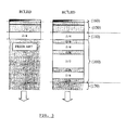
- Figure 1 shows a first stack (100), comprising of a first substack (120), a second substack (130). Said first and second substacks are separated by a third substack (140). Said substacks comprise of dielectric layers.
- a second stack (110) of dielectric layers is present, said second stack being attached to said first stack.
- a electromagnetic generating layer (150) is attached to said second stack.
- a third structure (160) is attached, said third structure can be but is not limited to be a metal reflector or a grating.
- Figure 2 shows the TE reflectance, both amplitude (%) and phase (deg), of the system comprising said first stack and said second stack for normal incidence of said beam from the direction of said second stack.
- the full line shows the present invention
- the dashed line shows the reflectance of a traditional DBR mirror.
- the negative equivalent penetration depth or negative phase is characteristic for the invention.
- Figure 3 shows on the left prior art RCLED's and one the invented system, comprising a metal reflector, an electromagnetic radiation generating layer or cavity, a second stack, here comprising of one dielectric layer, a first stack comprising a first substack, a second substack and a third substack. Said first and second substacks comprising here of three dielectric layers, said third substack, comprising one dielectric layer. Said system is attached to a substrate (170).
- Figure 4 shows a schematic k-diagrams for a RCLED (prior art) (dotted line) and the invented system (full line).
- the negative equivalent penetration depth of the invented system results in at least more than one crossing of the circle representing spontaneous emission and the reflection characteristic of the system. Therefore at least more than one resonance condition is found.
- Figure 5 shows an embodiment of the invention, exploiting a grating in order to enable resonance in a not normal direction.
- Said embodiment comprising of said first stack, an electromagnetic radiation generating layer and a grating.
- said first stack is transparent for normal incidence and highly reflective for not normal incidence, such decoupling between resonance in one direction and transporting the resulting electromagnetic radiation outside the cavity (180) towards the substrate (170) is enabled.
- the invented system guides a beam of electromagnetic radiation. Said guiding of a beam can also be denoted transferring of a beam.
- Said system comprises planar media.
- Said system comprises a stack of dielectric layers with a plurality of refractive indices and thicknesses of said layers.
- At least a first stack of dielectric layers with the following properties can be distinguished.
- Said first stack comprising at least a first substack, a second substack and a third substack, separating said first and second substacks.
- Said first substack comprises a plurality of dielectric layers
- said second substack comprises a plurality of dielectric layers. Dielectric layers of said first substack and said second substack having a same distance from said third substack are related to each other in the sense that at least they have the same refractive index.
- the sum of the thickness of dielectric layers of said first substack and said second substack having a same distance from said third substack is a multiple of half of the vacuum wavelength of said beam divided by the refractive index of said dielectric layers of said first substack and said second substack having a same distance from said third substack.
- said first substack layers are denoted B layers
- said second substack layers are denoted D layers
- said third substack layers are denoted C layers.
- said third substack layer comprises 1 layer but the invention is not limited thereto.
- Said dielectric layers can be semiconducting material such as Al(x)Ga(1-x)As or InP but is not limited hereto.
- Dielectric layers with refractive indices in between 2.9 and 3.6 can be used but the invention is not limited hereto.
- the thicknesses d of the layers in said first (B) and second substack (D) satisfy the following relationships with n x designates said refractive index of layer x , while ⁇ 0 designates the vacuum wavelength of said beam.
- n x designates said refractive index of layer x
- ⁇ 0 designates the vacuum wavelength of said beam.
- the thickness d of said third substack C satisfies the relationship below.
- Said third substack comprises at least a dielectric layer with a refractive index n c with a thickness being equal to a multiple of half of the vacuum wavelength of said beam divided by n c .
- the normal incidence transfermatrix for said first stack is always the unit matrix, meaning that for said normal incidence said first stack is fully transparent or opaque.
- said system further comprises a second stack of dielectric layers.
- the number and thicknesses of the layers in said second stack are fully arbitrary.
- Figure 1 shows that said second stack is placed on top of said first stack and thus attached to said first stack.
- alternative placements of said first and second stack are possible, for instance the placement of said first stack and said second stack can be interchanged.
- said sequence of layers consisting of said first stack and second stack can be repeated an arbitrary number of times, if necessary with different material parameters in each repetition.
- said system comprises thus a periodic repetition of said first and said second stack.
- the refractive index of said dielectric layers are different for at least two repetitions.
- said system comprises at least a periodic repetition of said first stack.
- the refractive index of said dielectric layers are different for at least two repetitions.
- the parameters of said stack of said dielectric layers, both said first stack and said second stack are chosen such that they cooperatively establish a high reflectance of said beam for off-axis incidence, a moderate reflectance of said beam for normal incidence and a negative equivalent penetration depth upon reflection of said beam.
- said first stack is designed for establishing a high reflectance of said beam for off-axis incidence and realizing a negative equivalent penetration depth upon reflection of said beam
- said second stack is designed for moderate reflectance of said beam for normal incidence.
- said second stack of dielectric layers can be characterised as being substantially reflective for normal incidence radiation.
- Said first stack of dielectric layers can be characterised as being substantially transparent for normal incidence radiation and substantially reflective for off-axis incidence radiation.
- a spatial decoupling of the functionalities can thus be recognized.
- the exploitation of the phase characteristic of said reflectance of such systems is not known in the art.
- said parameters of said first stack are chosen such that the reflectance of said beam is zero for normal incidence, while being very high for off-axis incidence.
- said stack exhibiting said high off-axis incidence reflectance, said moderate normal incidence reflectance and said negative equivalent penetration depth replaces a traditional DBR reflector in a microcavity light emitting diode.
- Said high off-axis incidence reflectance provides for a narrow radiation pattern, while said negative equivalent penetration depth creates additional resonances in the extraction cone, thereby boosting the extraction efficiency.
- said reflectance as a function of angle of said stack is such that the existence of leaky modes is greatly suppressed, thereby increasing the efficiency of the photon recycling mechanism.
- Such system can be characterised in that it comprises at least one electromagnetic generating layer. Further said electromagnetic generating layer is attached at one side to said second stack of dielectric layers. The system is thus being adapted for operating as an electromagnetic emitting device.
- said first stack exhibiting said zero normal incidence reflectance and said high off-axis incidence reflectance is used as a zero-loss outcoupling mirror in a surface emitting microcavity device.
- another periodic structure couples one or more guided modes to modes propagating in a direction being substantially normal to the surface. Said off-axis propagating guided modes experience high reflectance upon incidence of said outcoupling mirror, thereby leading to high cavity Q-factors.
- said second stack of dielectric layers comprises an alternating sequence of dielectric layers with refractive indices n 1 and n 2 .
- the thickness of each of said dielectric layers are a quarter of the vacuum wavelength of said beam divided by the refractive index of the corresponding dielectric layer.
- Said second stack of dielectric layers can be characterised as a traditional DBR stack of alternating layers with refractive indices n 1 and n 2 , each having an optical thickness of a quarter wavelength.
- said second stack of dielectric layers consists of a dielectric layer with refractive index n 1 and the thickness of said dielectric layer being a quarter of the vacuum wavelength of said beam divided by n 1 .
- the first substack (B) of said first stack consists of a DBR with the same materials as said second substack, thus having said indices n 1 and n 2 .
- Said first substack has an odd total number of layers m .
- Said third substack (C) has an optical thickness of half a wavelength, while said second substack (D) is then the mirror image of said first substack (B).
- said second stack consists of a single quarter-wavelength-layer (A) of material with said index n 1
- said first substack (B) consists of three quarter-wavelength-layers of alternating said indices n 2 -n 1 -n 2
- Said third substack (C) is a half-wavelength-layer of material with said index n 1
- said second substack (D) has the same structure as said first substack (B).
- Figure 2 compares the reflection characteristics of said stack consisting of said sub-stacks A,B,C and D with those of a traditional DBR structure containing only said stack A and not said stacks B, C nor D. Both structures are embedded in a medium with said index n 1 .
- said first stack and said second stack are not repeated, the invention is not limited thereto.
- the present invention yields much higher reflectivitities for off-axis incidence, while still maintaining the possibility of an arbitrary reflectance for normal incidence by choosing the number of layers in said second stack A.
- the slope of said reflection characteristic as a function of incidence angle of said beam is different for the present invention as compared to a said traditional DBR, leading to a negative equivalent penetration depth.
- said structure from said fourth embodiment replaces a traditional DBR mirror in a microcavity light emitting device.
- This device is henceforth referred to as a RC 2 LED, while the known device with said DBR reflector is referred to as a RCLED.
- This device is henceforth referred to as a RC2LED, while the known device with said DBR reflector is referred to as a RCLED.
- Said name RC2LED stems from the presence of two resonant cavities (RC), one containing the electromagnetic generating region as in said RCLED, and one RC used in the reflector. The general properties of said two classes of devices are compared using the specific but not limiting examples of the devices outlined in Figure 3.
- the optical properties of said RCLED and said RC 2 LED as outlined in said specific but not limiting example of fig. 3 were simulated assuming emitting dipoles oriented parallel to the interface in said stack, said dipoles having gaussian spontaneous emission spectrum with a FWHM of 45 nm centered at 980 nm, in the absence of a AR coating on the substrate and in the absence of the photon recycling effect. Both devices exhibit an extraction efficiency of about 18 %, but the radiation pattern of said RC 2 LED is much narrower. For said RCLED, only 34 % of the light emitted into air falls within a NA of 0.5, whereas for said RC 2 LED this figure is as high as 52 %.
- phase of the reflection of said structure for normal incidence as a function of wavelength also exhibits a negative slope. This creates extra resonances in the wavelength domain, leading to an optical spectrum with multiple peaks.
- said RC 2 LED the presence of leaky modes is significantly suppressed as compared to said traditional RCLEDs, even when said RCLEDs use a larger number of pairs in said DBR. This increases the efficiency of the photon recycling effect. Note that the same degrees of freedom for device design such as changing the cavity length or changing the position of the active layer apply equally well to said RC 2 LED as to said RCLED.
- said second stack of dielectric layers is not present, leading to a structure, comprising said first stack, which is fully transparent for normal incidence of said beam, but exhibiting a high off-axis reflectance of said beam.
- the stack from the fifth embodiment is employed as a zero-loss outcoupling mirror in a surface emitting microcavity device.
- Said microcavity device furthermore contains a periodic structure coupling one or more guided modes to modes propagating in a direction being substantially normal to the surface.
- Said off-axis propagating guided modes experience high reflectance upon incidence of said outcoupling mirror, thereby leading to high cavity Q-factors, but at the same time providing for very low outcoupling loss.
- the invented system can be described as a system for transferring a beam of electromagnetic radiation, said system comprising a stack of dielectric media with a plurality of refractive indices and thicknesses, said stack of said dielectric media containing one or more substacks exhibiting transparency upon normal incidence of said dielectric beam, the parameters of said system further being chosen such that they can cooperatively establish high reflectance upon off-axis incidence of said beam, arbitrary reflectance upon normal incidence of said beam and negative equivalent penetration depth of said beam.
- Said stack can be used as a mirror in a microcavity device.
- Said stack can also used as a mirror in a microcavity light emitting diode. Said mirror provides for a narrow radiation pattern and/or a high extraction efficiency.
- said invented sytem can be described as a system for transferring a beam of electromagnetic radiation, said system comprising a stack of dielectric media with a plurality of refractive indices and thicknesses, the parameters of said system further being chosen such that said stack of said dielectric media is fully transparent for normal incidence of said dielectric beam and such that said stack of said dielectric media has high reflectance for off-axis incidence.
- Said stack can again be used as a mirror in a microcavity device or as an outcoupling mirror in a surface emitting microcavity device.
- said device can further contain a periodic structure coupling one or more guided modes to modes propagating in a direction being substantially normal to the surface.
- Said electromagnetic radiation in the invention can be in the range of microwave radiation.
- Said system can also be integrated in microwave antenna's.
Landscapes
- Electroluminescent Light Sources (AREA)
- Optical Couplings Of Light Guides (AREA)
Abstract
Description
Claims (23)
- A system for guiding a beam of electromagnetic radiation, said system comprising at least a first stack of dielectric layers, said first stack comprising at least a first substack, a second substack and a third substack, separating said first and second substack, said first substack comprises at least one dielectric layer, said second substack comprises at least one dielectric layer, said third substack comprises at least one dielectric layer, dielectric layers of said first substack and said second substack having a same distance from said third substack, have the same refractive index and the sum of the thickness of dielectric layers of said first substack and said second substack having a same distance from said third substack is a multiple of half of the vacuum wavelength of said beam divided by the refractive index of said dielectric layers of said first substack and said second substack having a same distance from said third substack, said third substack thickness being substantially different from a quarter of the vacuum wavelength of said beam divided by the refractive index of said one dielectric layer of said third substack and wherein said first substack and said second substack each have an odd number of layers.
- The system as recited in 1, wherein said first substack and said second substack comprise dielectric layers with refractive indices n1 and n2.
- The system as recited in 1, wherein said refractive indices are substantially different such that the equivalent penetration depth of said beam is negative.
- The system as recited in 3, wherein said first substack comprises a first and second layer with refractive index n2, a third layer with refractive index n1, said first and said third layer being attached to each other, said second and said third layer being attached to each other, said first and said second layer not being attached to each other.
- The system as recited in 3, wherein said first substack being a concatenation of a first layer with refractive index n2, a second layer with refractive index n1 and a third layer with refractive layer n2.
- The system as recited in 5, wherein said third substack being a dielectric layer with index n1.
- A system for guiding a beam of electromagnetic radiation, said system comprising at least a first stack of dielectric layers, said first stack comprising at least a first substack, a second substack and a third substack, separating said first and second substack, said first substack comprises at least one dielectric layer, said second substack comprises at least one dielectric layer, said third substack comprises at least one dielectric layer, dielectric layers of said first substack and said second substack having a same distance from said third substack, have the same refractive index and the sum of the thickness of dielectric layers of said first substack and said second substack having a same distance from said third substack is a multiple of half of the vacuum wavelength of said beam divided by the refractive index of said dielectric layers of said first substack and said second substack having a same distance from said third substack, said third substack thickness being substantially different from a quarter of the vacuum wavelength of said beam divided by the refractive index of said one dielectric layer of said third substack, wherein said first stack of dielectric layers is substantially transparant for normal incidence radiation and substantially reflective for off-axis incidence radiation.
- A system for guiding a beam of electromagnetic radiation, said system comprising at least a first stack of dielectric layers, said first stack comprising at least a first substack, a second substack and a third substack, separating said first and second substack, said first substack comprises at least one dielectric layer, said second substack comprises at least one dielectric layer, said third substack comprises at least one dielectric layer, dielectric layers of said first substack and said second substack having a same distance from said third substack, have the same refractive index and the sum of the thickness of dielectric layers of said first substack and said second substack having a same distance from said third substack is a multiple of half of the vacuum wavelength of said beam divided by the refractive index of said dielectric layers of said first substack and said second substack having a same distance from said third substack, said third substack thickness being substantially different from a quarter of the vacuum wavelength of said beam divided by the refractive index of said one dielectric layer of said third substack, and comprising a periodic repetition of at least one of said stacks.
- The system as recited in 8, comprising a periodic repetition of said first and said second stack.
- The system as recited in 9, wherein the refractive index of said dielectric layers is different for at least two repetitions.
- The system as recited in 8, comprising at least a periodic repetition of said first stack.
- The system as recited in 11, wherein the refractive index of said dielectric layers is different for at least two repetitions.
- A system for guiding a beam of electromagnetic radiation, said system comprising at least a first stack of dielectric layers, said first stack comprising at least a first substack, a second substack and a third substack, separating said first and second substack, said first substack comprises at least one dielectric layer, said second substack comprises at least one dielectric layer, said third substack comprises at least one dielectric layer, dielectric layers of said first substack and said second substack having a same distance from said third substack, have the same refractive index and the sum of the thickness of dielectric layers of said first substack and said second substack having a same distance from said third substack is a multiple of half of the vacuum wavelength of said beam divided by the refractive index of said dielectric layers of said first substack and said second substack having a same distance from said third substack, said third substack thickness being substantially different from a quarter of the vacuum wavelength of said beam divided by the refractive index of said one dielectric layer of said third substack, wherein said second stack of dielectric layers consists of a dielectric layer with refractive index n1 and the thickness of said dielectric layer is a quarter of the vacuum wavelength of said beam divided by n1.
- A system for guiding a beam of electromagnetic radiation, said system comprising at least a first stack of dielectric layers, said first stack comprising at least a first substack, a second substack and a third substack, separating said first and second substack, said first substack comprises at least one dielectric layer, said second substack comprises at least one dielectric layer, said third substack comprises at least one dielectric layer, dielectric layers of said first substack and said second substack having a same distance from said third substack, have the same refractive index and the sum of the thickness of dielectric layers of said first substack and said second substack having a same distance from said third substack is a multiple of half of the vacuum wavelength of said beam divided by the refractive index of said dielectric layers of said first substack and said second substack having a same distance from said third substack, said third substack thickness being substantially different from a quarter of the vacuum wavelength of said beam divided by the refractive index of said one dielectric layer of said third substack, and comprising a second stack of dielectric layers, said second stack of dielectric layers being substantially reflective for normal incidence radiation.
- The system as recited in 14, wherein said reflectivity of said second stack being within the range of 40 to 70 %.
- The system as recited in 14, wherein said reflectivity of said second stack being approximately 60%.
- A system for guiding a beam of electromagnetic radiation, said system comprising at least a first stack of dielectric layers, said first stack comprising at least a first substack, a second substack and a third substack, separating said first and second substack, said first substack comprises at least one dielectric layer, said second substack comprises at least one dielectric layer, said third substack comprises at least one dielectric layer, dielectric layers of said first substack and said second substack having a same distance from said third substack, have the same refractive index and the sum of the thickness of dielectric layers of said first substack and said second substack having a same distance from said third substack is a multiple of half of the vacuum wavelength of said beam divided by the refractive index of said dielectric layers of said first substack and said second substack having a same distance from said third substack, said third substack thickness being substantially different from a quarter of the vacuum wavelength of said beam divided by the refractive index of said one dielectric layer of said third substack, and said first stack of dielectric layers having a normal incidence matrix being substantially equal to the unit matrix.
- A system for guiding a beam of electromagnetic radiation, said system comprising at least a first stack of dielectric layers, said first stack comprising at least a first substack, a second substack and a third substack, separating said first and second substack, said first substack comprises at least one dielectric layer, said second substack comprises at least one dielectric layer, said third substack comprises at least one dielectric layer, dielectric layers of said first substack and said second substack having a same distance from said third substack, have the same refractive index and the sum of the thickness of dielectric layers of said first substack and said second substack having a same distance from said third substack is a multiple of half of the vacuum wavelength of said beam divided by the refractive index of said dielectric layers of said first substack and said second substack having a same distance from said third substack, said third substack thickness being substantially different from a quarter of the vacuum wavelength of said beam divided by the refractive index of said one dielectric layer of said third substack, and comprising a second stack of dielectric layers and at least one electromagnetic generating layer, said system having a narrow radiation pattern.
- A system for guiding a beam of electromagnetic radiation, said system comprising at least a first stack of dielectric layers, said first stack comprising at least a first substack, a second substack and a third substack, separating said first and second substack, said first substack comprises at least one dielectric layer, said second substack comprises at least one dielectric layer, said third substack comprises at least one dielectric layer, dielectric layers of said first substack and said second substack having a same distance from said third substack, have the same refractive index and the sum of the thickness of dielectric layers of said first substack and said second substack having a same distance from said third substack is a multiple of half of the vacuum wavelength of said beam divided by the refractive index of said dielectric layers of said first substack and said second substack having a same distance from said third substack, said third substack thickness being substantially different from a quarter of the vacuum wavelength of said beam divided by the refractive index of said one dielectric layer of said third substack, and wherein at least one layer of said first or second stack has a thickness substantially different from a quarter of the vacuum wavelength of said beam divided by the refractive index of said layer of said first or second stack.
- A system for guiding a beam of electromagnetic radiation, said system comprising at least a first stack of dielectric layers, said first stack comprising at least a first substack, a second substack and a third substack, separating said first and second substack, said first substack comprises at least one dielectric layer, said second substack comprises at least one dielectric layer, said third substack comprises at least one dielectric layer, dielectric layers of said first substack and said second substack having a same distance from said third substack, have the same refractive index and the sum of the thickness of dielectric layers of said first substack and said second substack having a same distance from said third substack is a multiple of half of the vacuum wavelength of said beam divided by the refractive index of said dielectric layers of said first substack and said second substack having a same distance from said third substack, said third substack thickness being substantially different from a quarter of the vacuum wavelength of said beam divided by the refractive index of said one dielectric layer of said third substack, and said third substack consisting of a single dielectric layer with a refractive index nc with a thickness equal to a multiple of half of the vacuum wavelength of said beam divided by nc.
- A method for generating a first beam of electromagnetic radiation with a narrow radiation pattern, comprising the steps:providing a system such as in claim 1,generating a second beam of electromagnetic radiation with a wide radiation pattern;letting said second beam resonate in between a first and a second structure; wherein said first structure being substantially transparent for normal incidence of said second beam on said first structure and substantially reflective for off-axis incidence of said second beam and said second structure being adapted for partly reflecting said second beam in a off-axis direction; and said part of said second beam being transferred through said first structure being said first beam.
- A method for generating a first beam of electromagnetic radiation with a narrow radiation pattern, comprising the steps:providing a system such as in claim 1,generating a second beam of electromagnetic radiation with a wide radiation pattern;letting said second beam resonate in between a first and a second structure; wherein said first structure being substantially transparent for normal incidence of said second beam on said first structure and said first structure being adapted for having a negative equivalent penetration depth; andsaid part of said second beam being transferred through said first structure being said first beam.
- A method for generating a first beam of electromagnetic radiation with a narrow radiation pattern, comprising the steps:generating a second beam of electromagnetic radiation with a wide radiation pattern;letting said second beam resonate in between a first and a second structure; wherein said first structure comprising a first substructure and a second substructure, said first substructure being substantially reflective for normal incidence for normal incidence of said second beam, said second substructure being substantially reflective for off-axis incidence of said second beam and substantially transparent for normal incidence of said second beam; and said part of said second beam being transferred through said first structure being said first beam.
Priority Applications (1)
| Application Number | Priority Date | Filing Date | Title |
|---|---|---|---|
| EP00870255A EP1098374B1 (en) | 1999-11-05 | 2000-10-31 | Optical filter and Resonant Cavity LED comprising the said optical filter |
Applications Claiming Priority (3)
| Application Number | Priority Date | Filing Date | Title |
|---|---|---|---|
| EP99870231 | 1999-11-05 | ||
| EP99870231A EP1098375A1 (en) | 1999-11-05 | 1999-11-05 | Optical filter and Resonant Cavity LED comprising the said optical filter |
| EP00870255A EP1098374B1 (en) | 1999-11-05 | 2000-10-31 | Optical filter and Resonant Cavity LED comprising the said optical filter |
Publications (3)
| Publication Number | Publication Date |
|---|---|
| EP1098374A2 true EP1098374A2 (en) | 2001-05-09 |
| EP1098374A3 EP1098374A3 (en) | 2002-09-18 |
| EP1098374B1 EP1098374B1 (en) | 2004-09-08 |
Family
ID=26074307
Family Applications (1)
| Application Number | Title | Priority Date | Filing Date |
|---|---|---|---|
| EP00870255A Expired - Lifetime EP1098374B1 (en) | 1999-11-05 | 2000-10-31 | Optical filter and Resonant Cavity LED comprising the said optical filter |
Country Status (1)
| Country | Link |
|---|---|
| EP (1) | EP1098374B1 (en) |
Family Cites Families (3)
| Publication number | Priority date | Publication date | Assignee | Title |
|---|---|---|---|---|
| US4756602A (en) * | 1987-06-05 | 1988-07-12 | Rockwell International Corporation | Narrowband optical filter with partitioned cavity |
| US5144498A (en) * | 1990-02-14 | 1992-09-01 | Hewlett-Packard Company | Variable wavelength light filter and sensor system |
| US5226053A (en) * | 1991-12-27 | 1993-07-06 | At&T Bell Laboratories | Light emitting diode |
-
2000
- 2000-10-31 EP EP00870255A patent/EP1098374B1/en not_active Expired - Lifetime
Also Published As
| Publication number | Publication date |
|---|---|
| EP1098374A3 (en) | 2002-09-18 |
| EP1098374B1 (en) | 2004-09-08 |
Similar Documents
| Publication | Publication Date | Title |
|---|---|---|
| US8212273B2 (en) | Vertical LED with conductive vias | |
| US11757066B2 (en) | LED emitters with integrated nano-photonic structures to enhance EQE | |
| US9178119B2 (en) | Vertical light emitting diodes | |
| Barnes | Electromagnetic crystals for surface plasmon polaritons and the extraction of light from emissive devices | |
| KR101404529B1 (en) | Plasmon enhanced light-emitting diodes | |
| KR101133380B1 (en) | Surface emitting laser | |
| KR101600633B1 (en) | Laser light source and method for producing a laser light source | |
| GB2304230A (en) | Light emitting diodes | |
| US20070029560A1 (en) | Light-emitting devices with high extraction efficiency | |
| JP2003504880A (en) | Polarization control of vertical cavity surface emitting laser | |
| Baets et al. | Resonant-cavity light-emitting diodes: a review | |
| US5617445A (en) | Quantum cavity light emitting element | |
| JPH05506518A (en) | Fabry-Perot modulator | |
| EP1298461A1 (en) | Distributed Bragg reflector comprising GaP and a semiconductor resonant cavity device comprising such DBR | |
| US6548824B2 (en) | Semiconductor light emitting device for stably obtaining peak wave length of emission spectrum | |
| JP2005159002A (en) | Light receiving element, optical module, and optical transmission device | |
| US11448824B2 (en) | Devices with semiconductor hyperbolic metamaterials | |
| KR100413708B1 (en) | Microcavity LED photon recycling | |
| EP1098375A1 (en) | Optical filter and Resonant Cavity LED comprising the said optical filter | |
| US20060157723A1 (en) | Light emitting device | |
| EP0785601A1 (en) | Visible VCSEL with hybrid mirrors | |
| US6603605B1 (en) | System for guiding a beam of electromagnetic radiation | |
| EP1098374B1 (en) | Optical filter and Resonant Cavity LED comprising the said optical filter | |
| US11482652B2 (en) | Method for producing an extraction-layer light-emitting diode comprising a step of dimensioning a semiconductor layer | |
| KR0167086B1 (en) | Fabry-perot modulator and modulating method |
Legal Events
| Date | Code | Title | Description |
|---|---|---|---|
| PUAI | Public reference made under article 153(3) epc to a published international application that has entered the european phase |
Free format text: ORIGINAL CODE: 0009012 |
|
| AK | Designated contracting states |
Kind code of ref document: A2 Designated state(s): AT BE CH CY DE DK ES FI FR GB GR IE IT LI LU MC NL PT SE |
|
| AX | Request for extension of the european patent |
Free format text: AL;LT;LV;MK;RO;SI |
|
| PUAL | Search report despatched |
Free format text: ORIGINAL CODE: 0009013 |
|
| AK | Designated contracting states |
Kind code of ref document: A3 Designated state(s): AT BE CH CY DE DK ES FI FR GB GR IE IT LI LU MC NL PT SE |
|
| AX | Request for extension of the european patent |
Free format text: AL;LT;LV;MK;RO;SI |
|
| 17P | Request for examination filed |
Effective date: 20021113 |
|
| AKX | Designation fees paid |
Designated state(s): BE DE FR GB |
|
| 17Q | First examination report despatched |
Effective date: 20030605 |
|
| GRAP | Despatch of communication of intention to grant a patent |
Free format text: ORIGINAL CODE: EPIDOSNIGR1 |
|
| GRAS | Grant fee paid |
Free format text: ORIGINAL CODE: EPIDOSNIGR3 |
|
| GRAA | (expected) grant |
Free format text: ORIGINAL CODE: 0009210 |
|
| AK | Designated contracting states |
Kind code of ref document: B1 Designated state(s): BE DE FR GB |
|
| PG25 | Lapsed in a contracting state [announced via postgrant information from national office to epo] |
Ref country code: BE Free format text: LAPSE BECAUSE OF FAILURE TO SUBMIT A TRANSLATION OF THE DESCRIPTION OR TO PAY THE FEE WITHIN THE PRESCRIBED TIME-LIMIT Effective date: 20040908 |
|
| REG | Reference to a national code |
Ref country code: GB Ref legal event code: FG4D |
|
| REG | Reference to a national code |
Ref country code: IE Ref legal event code: FG4D |
|
| REF | Corresponds to: |
Ref document number: 60013534 Country of ref document: DE Date of ref document: 20041014 Kind code of ref document: P |
|
| PLBE | No opposition filed within time limit |
Free format text: ORIGINAL CODE: 0009261 |
|
| STAA | Information on the status of an ep patent application or granted ep patent |
Free format text: STATUS: NO OPPOSITION FILED WITHIN TIME LIMIT |
|
| ET | Fr: translation filed | ||
| 26N | No opposition filed |
Effective date: 20050609 |
|
| PGFP | Annual fee paid to national office [announced via postgrant information from national office to epo] |
Ref country code: GB Payment date: 20120924 Year of fee payment: 13 |
|
| PGFP | Annual fee paid to national office [announced via postgrant information from national office to epo] |
Ref country code: FR Payment date: 20121115 Year of fee payment: 13 Ref country code: DE Payment date: 20120924 Year of fee payment: 13 |
|
| GBPC | Gb: european patent ceased through non-payment of renewal fee |
Effective date: 20131031 |
|
| PG25 | Lapsed in a contracting state [announced via postgrant information from national office to epo] |
Ref country code: GB Free format text: LAPSE BECAUSE OF NON-PAYMENT OF DUE FEES Effective date: 20131031 |
|
| REG | Reference to a national code |
Ref country code: FR Ref legal event code: ST Effective date: 20140630 |
|
| REG | Reference to a national code |
Ref country code: DE Ref legal event code: R119 Ref document number: 60013534 Country of ref document: DE Effective date: 20140501 |
|
| PG25 | Lapsed in a contracting state [announced via postgrant information from national office to epo] |
Ref country code: DE Free format text: LAPSE BECAUSE OF NON-PAYMENT OF DUE FEES Effective date: 20140501 Ref country code: FR Free format text: LAPSE BECAUSE OF NON-PAYMENT OF DUE FEES Effective date: 20131031 |