EP1098363A2 - Testing integrated circuits - Google Patents
Testing integrated circuits Download PDFInfo
- Publication number
- EP1098363A2 EP1098363A2 EP00309584A EP00309584A EP1098363A2 EP 1098363 A2 EP1098363 A2 EP 1098363A2 EP 00309584 A EP00309584 A EP 00309584A EP 00309584 A EP00309584 A EP 00309584A EP 1098363 A2 EP1098363 A2 EP 1098363A2
- Authority
- EP
- European Patent Office
- Prior art keywords
- substrate
- array
- regions
- interconnection
- contact pads
- Prior art date
- Legal status (The legal status is an assumption and is not a legal conclusion. Google has not performed a legal analysis and makes no representation as to the accuracy of the status listed.)
- Withdrawn
Links
Images



Classifications
-
- H—ELECTRICITY
- H10—SEMICONDUCTOR DEVICES; ELECTRIC SOLID-STATE DEVICES NOT OTHERWISE PROVIDED FOR
- H10W—GENERIC PACKAGES, INTERCONNECTIONS, CONNECTORS OR OTHER CONSTRUCTIONAL DETAILS OF DEVICES COVERED BY CLASS H10
- H10W72/00—Interconnections or connectors in packages
- H10W72/20—Bump connectors, e.g. solder bumps or copper pillars; Dummy bumps; Thermal bumps
-
- H—ELECTRICITY
- H10—SEMICONDUCTOR DEVICES; ELECTRIC SOLID-STATE DEVICES NOT OTHERWISE PROVIDED FOR
- H10W—GENERIC PACKAGES, INTERCONNECTIONS, CONNECTORS OR OTHER CONSTRUCTIONAL DETAILS OF DEVICES COVERED BY CLASS H10
- H10W72/00—Interconnections or connectors in packages
- H10W72/071—Connecting or disconnecting
-
- H—ELECTRICITY
- H10—SEMICONDUCTOR DEVICES; ELECTRIC SOLID-STATE DEVICES NOT OTHERWISE PROVIDED FOR
- H10W—GENERIC PACKAGES, INTERCONNECTIONS, CONNECTORS OR OTHER CONSTRUCTIONAL DETAILS OF DEVICES COVERED BY CLASS H10
- H10W72/00—Interconnections or connectors in packages
- H10W72/851—Dispositions of multiple connectors or interconnections
-
- H—ELECTRICITY
- H10—SEMICONDUCTOR DEVICES; ELECTRIC SOLID-STATE DEVICES NOT OTHERWISE PROVIDED FOR
- H10W—GENERIC PACKAGES, INTERCONNECTIONS, CONNECTORS OR OTHER CONSTRUCTIONAL DETAILS OF DEVICES COVERED BY CLASS H10
- H10W70/00—Package substrates; Interposers; Redistribution layers [RDL]
- H10W70/60—Insulating or insulated package substrates; Interposers; Redistribution layers
-
- H—ELECTRICITY
- H10—SEMICONDUCTOR DEVICES; ELECTRIC SOLID-STATE DEVICES NOT OTHERWISE PROVIDED FOR
- H10W—GENERIC PACKAGES, INTERCONNECTIONS, CONNECTORS OR OTHER CONSTRUCTIONAL DETAILS OF DEVICES COVERED BY CLASS H10
- H10W72/00—Interconnections or connectors in packages
- H10W72/071—Connecting or disconnecting
- H10W72/072—Connecting or disconnecting of bump connectors
- H10W72/07231—Techniques
- H10W72/07236—Soldering or alloying
-
- H—ELECTRICITY
- H10—SEMICONDUCTOR DEVICES; ELECTRIC SOLID-STATE DEVICES NOT OTHERWISE PROVIDED FOR
- H10W—GENERIC PACKAGES, INTERCONNECTIONS, CONNECTORS OR OTHER CONSTRUCTIONAL DETAILS OF DEVICES COVERED BY CLASS H10
- H10W72/00—Interconnections or connectors in packages
- H10W72/071—Connecting or disconnecting
- H10W72/072—Connecting or disconnecting of bump connectors
- H10W72/07251—Connecting or disconnecting of bump connectors characterised by changes in properties of the bump connectors during connecting
-
- H—ELECTRICITY
- H10—SEMICONDUCTOR DEVICES; ELECTRIC SOLID-STATE DEVICES NOT OTHERWISE PROVIDED FOR
- H10W—GENERIC PACKAGES, INTERCONNECTIONS, CONNECTORS OR OTHER CONSTRUCTIONAL DETAILS OF DEVICES COVERED BY CLASS H10
- H10W72/00—Interconnections or connectors in packages
- H10W72/071—Connecting or disconnecting
- H10W72/075—Connecting or disconnecting of bond wires
- H10W72/07531—Techniques
- H10W72/07532—Compression bonding, e.g. thermocompression bonding
-
- H—ELECTRICITY
- H10—SEMICONDUCTOR DEVICES; ELECTRIC SOLID-STATE DEVICES NOT OTHERWISE PROVIDED FOR
- H10W—GENERIC PACKAGES, INTERCONNECTIONS, CONNECTORS OR OTHER CONSTRUCTIONAL DETAILS OF DEVICES COVERED BY CLASS H10
- H10W72/00—Interconnections or connectors in packages
- H10W72/20—Bump connectors, e.g. solder bumps or copper pillars; Dummy bumps; Thermal bumps
- H10W72/251—Materials
-
- H—ELECTRICITY
- H10—SEMICONDUCTOR DEVICES; ELECTRIC SOLID-STATE DEVICES NOT OTHERWISE PROVIDED FOR
- H10W—GENERIC PACKAGES, INTERCONNECTIONS, CONNECTORS OR OTHER CONSTRUCTIONAL DETAILS OF DEVICES COVERED BY CLASS H10
- H10W72/00—Interconnections or connectors in packages
- H10W72/20—Bump connectors, e.g. solder bumps or copper pillars; Dummy bumps; Thermal bumps
- H10W72/29—Bond pads specially adapted therefor
-
- H—ELECTRICITY
- H10—SEMICONDUCTOR DEVICES; ELECTRIC SOLID-STATE DEVICES NOT OTHERWISE PROVIDED FOR
- H10W—GENERIC PACKAGES, INTERCONNECTIONS, CONNECTORS OR OTHER CONSTRUCTIONAL DETAILS OF DEVICES COVERED BY CLASS H10
- H10W72/00—Interconnections or connectors in packages
- H10W72/50—Bond wires
- H10W72/531—Shapes of wire connectors
- H10W72/536—Shapes of wire connectors the connected ends being ball-shaped
-
- H—ELECTRICITY
- H10—SEMICONDUCTOR DEVICES; ELECTRIC SOLID-STATE DEVICES NOT OTHERWISE PROVIDED FOR
- H10W—GENERIC PACKAGES, INTERCONNECTIONS, CONNECTORS OR OTHER CONSTRUCTIONAL DETAILS OF DEVICES COVERED BY CLASS H10
- H10W72/00—Interconnections or connectors in packages
- H10W72/50—Bond wires
- H10W72/531—Shapes of wire connectors
- H10W72/5363—Shapes of wire connectors the connected ends being wedge-shaped
-
- H—ELECTRICITY
- H10—SEMICONDUCTOR DEVICES; ELECTRIC SOLID-STATE DEVICES NOT OTHERWISE PROVIDED FOR
- H10W—GENERIC PACKAGES, INTERCONNECTIONS, CONNECTORS OR OTHER CONSTRUCTIONAL DETAILS OF DEVICES COVERED BY CLASS H10
- H10W72/00—Interconnections or connectors in packages
- H10W72/50—Bond wires
- H10W72/551—Materials of bond wires
- H10W72/552—Materials of bond wires comprising metals or metalloids, e.g. silver
- H10W72/5522—Materials of bond wires comprising metals or metalloids, e.g. silver comprising gold [Au]
-
- H—ELECTRICITY
- H10—SEMICONDUCTOR DEVICES; ELECTRIC SOLID-STATE DEVICES NOT OTHERWISE PROVIDED FOR
- H10W—GENERIC PACKAGES, INTERCONNECTIONS, CONNECTORS OR OTHER CONSTRUCTIONAL DETAILS OF DEVICES COVERED BY CLASS H10
- H10W72/00—Interconnections or connectors in packages
- H10W72/50—Bond wires
- H10W72/59—Bond pads specially adapted therefor
-
- H—ELECTRICITY
- H10—SEMICONDUCTOR DEVICES; ELECTRIC SOLID-STATE DEVICES NOT OTHERWISE PROVIDED FOR
- H10W—GENERIC PACKAGES, INTERCONNECTIONS, CONNECTORS OR OTHER CONSTRUCTIONAL DETAILS OF DEVICES COVERED BY CLASS H10
- H10W72/00—Interconnections or connectors in packages
- H10W72/90—Bond pads, in general
-
- H—ELECTRICITY
- H10—SEMICONDUCTOR DEVICES; ELECTRIC SOLID-STATE DEVICES NOT OTHERWISE PROVIDED FOR
- H10W—GENERIC PACKAGES, INTERCONNECTIONS, CONNECTORS OR OTHER CONSTRUCTIONAL DETAILS OF DEVICES COVERED BY CLASS H10
- H10W72/00—Interconnections or connectors in packages
- H10W72/90—Bond pads, in general
- H10W72/931—Shapes of bond pads
- H10W72/934—Cross-sectional shape, i.e. in side view
-
- H—ELECTRICITY
- H10—SEMICONDUCTOR DEVICES; ELECTRIC SOLID-STATE DEVICES NOT OTHERWISE PROVIDED FOR
- H10W—GENERIC PACKAGES, INTERCONNECTIONS, CONNECTORS OR OTHER CONSTRUCTIONAL DETAILS OF DEVICES COVERED BY CLASS H10
- H10W72/00—Interconnections or connectors in packages
- H10W72/90—Bond pads, in general
- H10W72/951—Materials of bond pads
- H10W72/952—Materials of bond pads comprising metals or metalloids, e.g. PbSn, Ag or Cu
-
- H—ELECTRICITY
- H10—SEMICONDUCTOR DEVICES; ELECTRIC SOLID-STATE DEVICES NOT OTHERWISE PROVIDED FOR
- H10W—GENERIC PACKAGES, INTERCONNECTIONS, CONNECTORS OR OTHER CONSTRUCTIONAL DETAILS OF DEVICES COVERED BY CLASS H10
- H10W90/00—Package configurations
- H10W90/701—Package configurations characterised by the relative positions of pads or connectors relative to package parts
- H10W90/751—Package configurations characterised by the relative positions of pads or connectors relative to package parts of bond wires
- H10W90/754—Package configurations characterised by the relative positions of pads or connectors relative to package parts of bond wires between a chip and a stacked insulating package substrate, interposer or RDL
Definitions
- This invention relates to techniques for testing semiconductor integrated circuit (IC) devices, and more specifically to testing wire bonded IC devices.
- MCM Multi-Chip-Module
- Burn-in tests are especially important for memory dies, which typically exhibit a 1-5% burn-in failure rate over dies that have been only functionally tested.
- burn-in tests require robust and reliable electrical probe connections. Consequently, it has been the pattern, where devices are mounted using solder bumps, to apply the solder bumps to the device, and employ special testing apparatus that electrically connects to the solder bumps.
- 09/366,388, filed 08/03/99 is the use of a silicon test bed in which a pattern of recesses is etched into a silicon wafer, and the recesses are interconnected to a test circuit that simulates the device circuit.
- the layout of recesses is made to accommodate the solder ball array on the IC device.
- the use of silicon as the test bed offers the advantages of high planarity, thermal properties that match the IC substrate, notably coefficient of thermal expansion, and the availability of a well developed interconnect technology for fabricating the test circuit.
- This test approach and test apparatus works well with IC chips or MCMs that are solder bump mounted, and have an array of solder bumps accessible for testing, but it appears inconsistent with IC devices that are packaged using wire bonds and have only pads accessible.
- Wire bond interconnections for integrated circuit devices have been widely used in IC packaging because they are relatively inexpensive and are highly reliable.
- burn-in testing IC devices after wire bonding is done in the final package and the die cannot be used for MCMs, and burn-in testing the dies before wire bonding using bare bonding pads is relatively ineffective.
- a state-of-the-art high pin count wire bonded IC package that avoids this problem is described and claimed in my co-pending application Serial No. 09/361,100, filed 07/01/99, which is incorporated herein by reference .
- This package uses an intermediate interconnection substrate (IIS) and the IC dies are bump mounted on the IIS.
- IIS intermediate interconnection substrate
- many IC packages still have IC dies that are directly wire bonded to the next interconnection level. It would be desirable to have a test procedure for burn-in testing of these IC dies that has the effectiveness and process integration compatibility of the burn-in test for bump-bonded devices.
- the wire bond pads are re-routed to bump-bond sites and the dies are provided with bump-bonds for the burn-in test.
- the KGD are packaged using either bump bonds or wire bonds, and can be mounted either face down for bump-bonding or face up for wire bonding.
- a semiconductor IC substrate 11 is shown with a standard IC contact pad 12 on the surface thereof.
- the substrate contains IC circuit elements (not shown).
- the semiconductor is typically silicon but may be a III-V semiconductor such as GaAs or InP for high speed transistors or photonic devices.
- the top metallization layer of the IC die includes contact pads for interconnection. In silicon based technology, these usually comprise aluminum. After the last metal level is defined and the contact pads formed, the top surface of the IC device is typically encapsulated with passivating layer 14.
- passivating materials are known and used, such as silicon nitride (SINCAPS), but the preferred choice is polyimide.
- a polyimide layer is easily patterned to expose the contact pads 12 as shown in Fig. 1.
- Photodefinable polymers can be used, and patterned using photolithography.
- a conductive runner 15, such as aluminum, is routed from contact pad 12 to another location on the surface of passivating layer 14.
- the runner 15 is covered with another insulating layer 16, such as polyimide.
- Layer 16 is patterned to expose the portion 17 of runner 15 at or near contact pad 12, and a second opening is made at another contact region to expose runner 15.
- the second opening is provided with Under Bump Metallization (UBM) 18 and solder bump 19.
- UBM Under Bump Metallization
- Wire bond 20 is shown contacting the portion of runner 15 over the contact pad 12. It is evident that solder bump 19 is electrically connected to contact pad 12, and can be used for burn-in testing of the IC using an array of conventional test probes.
- the wire bond site is shown directly over contact pad 12 but can be offset from the pad if desired.
- Fig. 2 shows substrate 21 with contact pad 22 on the surface thereof.
- the substrate is a portion of a standard semiconductor wafer. Processing according to this embodiment of the invention through the solder bump stage is performed at the wafer level. Testing may be at the wafer level or after singulation, as desired.
- Fig. 3 shows substrate 21 after deposition and patterning of polyimide layer 23. Layer 23 may be selectively applied by, e.g. screen printing, or may be applied by spin coating, and patterning using photolithography or other subtractive technique.
- conductive layer 24 is blanket deposited over the substrate by a suitable deposition technique such as sputtering, as shown in Fig. 4.
- Layer 24 is preferably aluminum but may be chosen from other conductive materials such as gold, gold alloy, TiPdAu, or may be formed as part of the UBM process in which case a UBM material such as CrCu may be used.
- the thickness of layer 24 may typically be in the range 0.3 - 3.0 ⁇ m.
- Layer 24 is patterned as indicated schematically in Fig. 4 to provide a conductive runner interconnecting contact pad 22 with a solder bump site indicated here at 26.
- the solder bump site 26 can be located anywhere on the surface of the substrate thereby providing the option of re-arranging the interconnection array of contact pads to another configuration represented by bump site 26. It is preferred that the solder bump site and the contact pad be located in relatively close proximity so as to minimize the length of IC interconnections.
- a second patterned polyimide layer 28 is selectively formed, as with layer 23, over the surface of the substrate and patterned to reveal region 26 - the solder bump site - of runner 24, and a second region 27 at or near contact pad 22.
- a UBM layer 31 is applied to solder bump site 26 as illustrated in Fig. 6.
- the material of runner 24 will typically be aluminum, and it is well known that aluminum is not a desirable material to solder. Consequently the practice in the industry is to apply a UBM coating on the portions of aluminum that are to be soldered, and reflow the solder to the UBM.
- the metal or metals used in UBM technology must adhere well to aluminum, be wettable by typical solder formulations, and be highly conductive.
- a structure meeting these requirements is a composite of chromium and copper. Chromium is deposited first, to adhere to the aluminum, and copper is applied over the chromium to provide a solder wettable surface. Chromium is known to adhere well to a variety of materials, organic as well as inorganic. Accordingly it adheres well to dielectric materials, e.g. SiO 2 , SINCAPS, polyimide, etc., commonly used in IC processing, as well as to metals such as copper and aluminum.
- solder alloys dissolve copper and de-wet from chromium. Therefore, a thin layer of copper directly on chromium will dissolve into the molten solder and the solder will then de-wet from the chromium layer. To insure interface integrity between the solder and the UBM, a composite or alloy layer of chromium and copper is typically used between the chromium and copper layers.
- the aforementioned layers are conventionally sputtered, so several options for depositing them are conveniently available.
- the layer can be sputtered from an alloy target. It can be sputtered using a chromium target, then changing to a copper target. Optionally it can be sputtered using separate chromium and copper targets, and transitioning between the two. The latter choice produces a layer with a graded composition, and is a preferred technique.
- runner 24 may be formed as part of the UBM process in which case runner 24 will comprise CrCuCr, or a suitable alternative.
- the wire bond site 27 may be coated with a material to which standard gold or gold alloy wires can be effectively thermocompression bonded.
- the preferred choice is aluminum, which in the sequence shown, is selectively applied to cover site 27. This step may be performed at any point in the sequence prior to the wire bonding step.
- solder bumps or solder balls 33 are then applied to the UBM.
- the solder bumps or balls are conventionally used for flip-chip mounting of IC dies, and can be formed by any suitable technique such as ball placement or solder paste printing.
- the thickness of a typical solder bump for this application is 5-30 mils. Examples of solder compositions that can be used successfully in the processes described here are given in the following table: composition Sn Pb Sb Ag solidus °C liquidus °C I 63 37 183 183 II 95 5 235 240 III 96.5 3.5 220 220
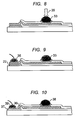
- the IC device can now be tested with both functional testing and burn-in testing by conventional probes represented by 35 in Fig. 8.
- the KGD are assembled in, e.g., an MCM package.
- the option of interconnecting the IC shown in the figures using wire bonding is schematically represented in Fig. 9, where both a solder bump 33, and a wire bond 35 are shown connected to the same electrical node, i.e. contact pad 22.
- the UBM layer can serve as the interconnection runner between the solder bumps and the IC contact pads.
- a relatively simple approach to this is to pattern the UBM layer to provide the UBM and the runner contacting the IC contact pads, but forming the runner so as to contact, e.g. overlap, the edge of the IC contact pads but not cover them. Reliable interconnection is thereby provided while leaving a suitable area of the aluminum contact pad for wire bonding.
- This approach is illustrated in Fig. 10 where layer 36 covers a portion of aluminum IC contact pad 37 and interconnects the pad to solder bump 38 but layer 36 leaves sufficient area of the pad uncovered to accommodate wire bond 39.
- IC device 41 is shown die bonded to an interconnection substrate 42, and wire bonded with wire 43 to an interconnection pattern 44 on substrate 42.
- the substrate may be an epoxy printed circuit board (PCB), or may be a ceramic or silicon interconnect substrate.
- the substrate may also be another active IC chip.
- the IC devices may be packaged or unpackaged.
- other KGD 51 are shown flip-chip bonded, with microbumps represented by 52, to multi-chip module (MCM) substrate 53.
- MCM substrate 53 may in turn be flip-chip mounted onto another interconnect substrate.
- the latter substrate may be an epoxy PCB with a cavity to accommodate device 51 in a recessed configuration.
- the pitch of contact pads for a bumped IC chip in current technology is of the order of 50-900 ⁇ m and the spacing between pads may be 20-500 ⁇ m.
- the bumps are typically 15-150 ⁇ m in height (z-direction).
- the IC device is usually square or rectangular with sides typically in the 2-20 mm range.
- the step of electrically testing the IC devices involves the application of test voltages to selected solder bumps on the IC die.
- IC devices would be conveyed from the singulation or packaging operation to a placement tool, then individually placed with the solder bumps aligned to the test array.
- the IC devices may be tested at the wafer level.
- the electrical test procedure itself is conventional and comprises the steps of applying test voltages to the test array, measuring the test voltages, comparing the measured test voltages to a set of predetermined IC device voltages, and selecting those IC devices with test voltages that meet said set of predetermined IC device voltages for final assembly, i.e. bonding the IC device to a permanent interconnection substrate.
- the steps of measuring, comparing and selecting are carried out by automated software driven means. For burn-in tests, the devices are typically exposed to an elevated temperature, e.g. 85-125 °C, prior to measuring.
Landscapes
- Testing Or Measuring Of Semiconductors Or The Like (AREA)
- Testing Of Individual Semiconductor Devices (AREA)
Abstract
Description
| composition | Sn | Pb | Sb | Ag | solidus °C | liquidus °C |
| I | 63 | 37 | 183 | 183 | ||
| II | 95 | 5 | 235 | 240 | ||
| III | 96.5 | 3.5 | 220 | 220 |
Claims (13)
- An integrated circuit (IC) device having an IC die wire bonded to a substrate said IC die having an array of solder bumps thereon.
- An integrated circuit (IC) device comprising:a. an integrated circuit die comprising a semiconductor substrate having an upper surface and a lower surface, and at least one IC device on said upper surface,b. an array of IC contact pads on said upper surface,c. an array of solder bumps on said upper surface, andd. metallization runners interconnecting said array of IC contact pads to said array of solder bumps.
- The IC device of claim 2 wherein the said substrate is silicon.
- The IC device of claim 2 further including an interconnection substrate supporting said semiconductor substrate, said interconnection substrate having an array of wire bonding pads, and wire bonds interconnecting the IC contact pads on said semiconductor substrate with the wire bonding pads on said interconnection substrate.
- A method for manufacturing an integrated circuit (IC) device comprising wire bonding an IC die to a substrate said IC die having an array of solder bumps thereon.
- A method for manufacturing an integrated circuit (IC) device comprising the steps of:a. forming an array of IC contact pads on a semiconductor IC device substrate, said IC device substrate having at least one IC device thereon,b. forming an interconnection runner interconnecting said array of IC contact pads to an array of solder bump sites,c. forming solder bumps on said solder bump sites,d. electrically testing said IC device by electrically contacting said solder bumps, ande. interconnecting said IC device substrate to an interconnection substrate using wire bond interconnections.
- The method of claim 6 wherein the step of electrically testing said IC device includes burn-in electrical testing.
- The method of claim 7 wherein said semiconductor IC device substrate is silicon.
- The method of claim 8 wherein said interconnection runner comprises aluminum.
- The method of claim 8 further including the step of applying under bump metallization (UBM) to said solder bump sites.
- The method of claim 10 wherein said interconnection runner and said UBM are formed in the same step.
- A method for manufacturing an IC device comprising the steps of:a. forming an array of IC contact pads on a semiconductor IC device substrate, said IC device substrate having at least one IC device thereon,b. depositing a polyimide layer to cover said IC device substrate except for at least a portion of said array of IC contact pads,c. depositing a conductive layer on said IC device substrate,d. patterning said conductive layer to form a plurality of first regions and a plurality of second regions, said first plurality of regions being connected to said second plurality of regions, and said first and second plurality of regions electrically connected to said array of IC contact pads,e. forming solder bumps on said first plurality of regions,f. electrically testing said IC device by electrically contacting said solder bumps, andg. interconnecting said IC device substrate to an interconnection substrate by wire bonding said second plurality of regions to said interconnection substrate.
- A method for manufacturing IC devices comprising the steps of:a. processing a group of IC devices by:i. forming an array of IC contact pads on a semiconductor IC device substrate, said IC device substrate having at least one IC device thereon,ii. depositing a polyimide layer to cover said IC device substrate except for at least a portion of said array of IC contact pads,iii. depositing a conductive layer on said IC device substrate,iv. patterning said conductive layer to form a plurality of first regions and a plurality of second regions, said first plurality of regions being connected to said second plurality of regions, and said first and second plurality of regions electrically connected to said array of IC contact pads,v. forming solder bumps on said first plurality of regions,vi. electrically testing said IC device by electrically contacting said solder bumps,b. interconnecting a first portion of said group of IC devices to an interconnection substrate by wire bonding said second plurality of regions to said interconnection substrate andc. interconnecting a second portion of said group of IC devices to an interconnection substrate by bump bonding said solder bumps on said first plurality of regions to said interconnection substrate.
Applications Claiming Priority (2)
| Application Number | Priority Date | Filing Date | Title |
|---|---|---|---|
| US435971 | 1999-11-08 | ||
| US09/435,971 US6342399B1 (en) | 1999-11-08 | 1999-11-08 | Testing integrated circuits |
Publications (2)
| Publication Number | Publication Date |
|---|---|
| EP1098363A2 true EP1098363A2 (en) | 2001-05-09 |
| EP1098363A3 EP1098363A3 (en) | 2004-01-21 |
Family
ID=23730575
Family Applications (1)
| Application Number | Title | Priority Date | Filing Date |
|---|---|---|---|
| EP00309584A Withdrawn EP1098363A3 (en) | 1999-11-08 | 2000-10-30 | Testing integrated circuits |
Country Status (6)
| Country | Link |
|---|---|
| US (2) | US6342399B1 (en) |
| EP (1) | EP1098363A3 (en) |
| JP (1) | JP2001201534A (en) |
| KR (1) | KR20010051538A (en) |
| SG (1) | SG124229A1 (en) |
| TW (1) | TW544829B (en) |
Cited By (1)
| Publication number | Priority date | Publication date | Assignee | Title |
|---|---|---|---|---|
| EP2380194A4 (en) * | 2008-12-19 | 2013-10-02 | Ati Technologies Ulc | FACE-TO-FACE (F2F) HYBRID STRUCTURE FOR INTEGRATED CIRCUIT |
Families Citing this family (12)
| Publication number | Priority date | Publication date | Assignee | Title |
|---|---|---|---|---|
| US6680213B2 (en) * | 2001-04-02 | 2004-01-20 | Micron Technology, Inc. | Method and system for fabricating contacts on semiconductor components |
| US7067916B2 (en) * | 2001-06-20 | 2006-06-27 | International Business Machines Corporation | Extension of fatigue life for C4 solder ball to chip connection |
| US6784556B2 (en) * | 2002-04-19 | 2004-08-31 | Kulicke & Soffa Investments, Inc. | Design of interconnection pads with separated probing and wire bonding regions |
| KR100585142B1 (en) * | 2004-05-04 | 2006-05-30 | 삼성전자주식회사 | Flip chip semiconductor package for bump test and manufacturing method thereof |
| US20070046314A1 (en) * | 2004-07-21 | 2007-03-01 | Advanced Semiconductor Engineering, Inc. | Process for testing IC wafer |
| DE102004047730B4 (en) * | 2004-09-30 | 2017-06-22 | Advanced Micro Devices, Inc. | A method for thinning semiconductor substrates for the production of thin semiconductor wafers |
| JP4639245B2 (en) * | 2008-05-22 | 2011-02-23 | パナソニック株式会社 | Semiconductor element and semiconductor device using the same |
| KR101006521B1 (en) * | 2008-06-30 | 2011-01-07 | 주식회사 하이닉스반도체 | Semiconductor package and manufacturing method thereof |
| US20100264522A1 (en) * | 2009-04-20 | 2010-10-21 | Chien-Pin Chen | Semiconductor device having at least one bump without overlapping specific pad or directly contacting specific pad |
| US8797057B2 (en) * | 2011-02-11 | 2014-08-05 | Taiwan Semiconductor Manufacturing Company, Ltd. | Testing of semiconductor chips with microbumps |
| US9391040B2 (en) | 2014-10-17 | 2016-07-12 | International Business Machines Corporation | Planarity-tolerant reworkable interconnect with integrated testing |
| KR102372355B1 (en) | 2015-08-26 | 2022-03-11 | 삼성전자주식회사 | Semiconductor chip, method for fabricating the same, and semiconductor package comprising the same |
Family Cites Families (13)
| Publication number | Priority date | Publication date | Assignee | Title |
|---|---|---|---|---|
| JPS5943553A (en) * | 1982-09-06 | 1984-03-10 | Hitachi Ltd | Electrode structure for semiconductor element |
| US5917707A (en) * | 1993-11-16 | 1999-06-29 | Formfactor, Inc. | Flexible contact structure with an electrically conductive shell |
| US5258330A (en) * | 1990-09-24 | 1993-11-02 | Tessera, Inc. | Semiconductor chip assemblies with fan-in leads |
| US5367763A (en) * | 1993-09-30 | 1994-11-29 | Atmel Corporation | TAB testing of area array interconnected chips |
| US5502333A (en) * | 1994-03-30 | 1996-03-26 | International Business Machines Corporation | Semiconductor stack structures and fabrication/sparing methods utilizing programmable spare circuit |
| US5554940A (en) * | 1994-07-05 | 1996-09-10 | Motorola, Inc. | Bumped semiconductor device and method for probing the same |
| US5517127A (en) * | 1995-01-09 | 1996-05-14 | International Business Machines Corporation | Additive structure and method for testing semiconductor wire bond dies |
| US5844317A (en) * | 1995-12-21 | 1998-12-01 | International Business Machines Corporation | Consolidated chip design for wire bond and flip-chip package technologies |
| US5969417A (en) * | 1996-08-27 | 1999-10-19 | Nec Corporation | Chip package device mountable on a mother board in whichever of facedown and wire bonding manners |
| US5783868A (en) * | 1996-09-20 | 1998-07-21 | Integrated Device Technology, Inc. | Extended bond pads with a plurality of perforations |
| US5918107A (en) * | 1998-04-13 | 1999-06-29 | Micron Technology, Inc. | Method and system for fabricating and testing assemblies containing wire bonded semiconductor dice |
| US6166556A (en) * | 1998-05-28 | 2000-12-26 | Motorola, Inc. | Method for testing a semiconductor device and semiconductor device tested thereby |
| US6511901B1 (en) * | 1999-11-05 | 2003-01-28 | Atmel Corporation | Metal redistribution layer having solderable pads and wire bondable pads |
-
1999
- 1999-11-08 US US09/435,971 patent/US6342399B1/en not_active Expired - Lifetime
-
2000
- 2000-10-30 EP EP00309584A patent/EP1098363A3/en not_active Withdrawn
- 2000-11-01 SG SG200006278A patent/SG124229A1/en unknown
- 2000-11-01 TW TW089122966A patent/TW544829B/en not_active IP Right Cessation
- 2000-11-08 KR KR1020000066196A patent/KR20010051538A/en not_active Withdrawn
- 2000-11-08 JP JP2000340172A patent/JP2001201534A/en active Pending
-
2001
- 2001-11-23 US US09/999,322 patent/US20020075031A1/en not_active Abandoned
Cited By (1)
| Publication number | Priority date | Publication date | Assignee | Title |
|---|---|---|---|---|
| EP2380194A4 (en) * | 2008-12-19 | 2013-10-02 | Ati Technologies Ulc | FACE-TO-FACE (F2F) HYBRID STRUCTURE FOR INTEGRATED CIRCUIT |
Also Published As
| Publication number | Publication date |
|---|---|
| TW544829B (en) | 2003-08-01 |
| KR20010051538A (en) | 2001-06-25 |
| JP2001201534A (en) | 2001-07-27 |
| US6342399B1 (en) | 2002-01-29 |
| US20020075031A1 (en) | 2002-06-20 |
| SG124229A1 (en) | 2006-08-30 |
| EP1098363A3 (en) | 2004-01-21 |
Similar Documents
| Publication | Publication Date | Title |
|---|---|---|
| US5532612A (en) | Methods and apparatus for test and burn-in of integrated circuit devices | |
| US5237130A (en) | Flip chip technology using electrically conductive polymers and dielectrics | |
| US5918364A (en) | Method of forming electrically conductive polymer interconnects on electrical substrates | |
| US6753208B1 (en) | Wafer scale method of packaging integrated circuit die | |
| US6459150B1 (en) | Electronic substrate having an aperture position through a substrate, conductive pads, and an insulating layer | |
| US8097947B2 (en) | Conductive systems and devices including wires coupled to anisotropic conductive film, and methods of forming the same | |
| US7087992B2 (en) | Multichip wafer level packages and computing systems incorporating same | |
| US6365501B2 (en) | Mask repattern process | |
| US6605525B2 (en) | Method for forming a wafer level package incorporating a multiplicity of elastomeric blocks and package formed | |
| US6372619B1 (en) | Method for fabricating wafer level chip scale package with discrete package encapsulation | |
| US6166556A (en) | Method for testing a semiconductor device and semiconductor device tested thereby | |
| EP0676091B1 (en) | Tab testing of area array interconnected chips | |
| EP0704895A2 (en) | Process for manufacturing semiconductor device and semiconductor wafer | |
| US5744383A (en) | Integrated circuit package fabrication method | |
| KR20040004761A (en) | Method of forming an integrated circuit package at a wafer level | |
| US6342399B1 (en) | Testing integrated circuits | |
| KR20020059851A (en) | Integrated circuit package formed at a wafer level | |
| DE10311368A1 (en) | Method for avoiding back-end rewiring in ball grid array packages and arrangement made therefrom | |
| US20050151268A1 (en) | Wafer-level assembly method for chip-size devices having flipped chips | |
| US6405429B1 (en) | Microbeam assembly and associated method for integrated circuit interconnection to substrates | |
| US6664176B2 (en) | Method of making pad-rerouting for integrated circuit chips | |
| US6536653B2 (en) | One-step bumping/bonding method for forming semiconductor packages | |
| US7215025B1 (en) | Wafer scale semiconductor structure | |
| JP2928484B2 (en) | Method and apparatus for testing IC chips | |
| US20020163069A1 (en) | Method for forming wafer level package having serpentine-shaped electrode along scribe line and package formed |
Legal Events
| Date | Code | Title | Description |
|---|---|---|---|
| PUAI | Public reference made under article 153(3) epc to a published international application that has entered the european phase |
Free format text: ORIGINAL CODE: 0009012 |
|
| AK | Designated contracting states |
Kind code of ref document: A2 Designated state(s): AT BE CH CY DE DK ES FI FR GB GR IE IT LI LU MC NL PT SE |
|
| AX | Request for extension of the european patent |
Free format text: AL;LT;LV;MK;RO;SI |
|
| PUAL | Search report despatched |
Free format text: ORIGINAL CODE: 0009013 |
|
| AK | Designated contracting states |
Kind code of ref document: A3 Designated state(s): AT BE CH CY DE DK ES FI FR GB GR IE IT LI LU MC NL PT SE |
|
| AX | Request for extension of the european patent |
Extension state: AL LT LV MK RO SI |
|
| RIC1 | Information provided on ipc code assigned before grant |
Ipc: 7H 01L 23/58 B Ipc: 7H 01L 21/66 A |
|
| 17P | Request for examination filed |
Effective date: 20040325 |
|
| 17Q | First examination report despatched |
Effective date: 20040427 |
|
| AKX | Designation fees paid |
Designated state(s): DE FR GB |
|
| STAA | Information on the status of an ep patent application or granted ep patent |
Free format text: STATUS: THE APPLICATION IS DEEMED TO BE WITHDRAWN |
|
| 18D | Application deemed to be withdrawn |
Effective date: 20041109 |