EP1098305A2 - Optical disk recording/reproducing device employing waveform correction of laser output signal - Google Patents
Optical disk recording/reproducing device employing waveform correction of laser output signal Download PDFInfo
- Publication number
- EP1098305A2 EP1098305A2 EP00309767A EP00309767A EP1098305A2 EP 1098305 A2 EP1098305 A2 EP 1098305A2 EP 00309767 A EP00309767 A EP 00309767A EP 00309767 A EP00309767 A EP 00309767A EP 1098305 A2 EP1098305 A2 EP 1098305A2
- Authority
- EP
- European Patent Office
- Prior art keywords
- level
- pulse signal
- average level
- signal
- basic pulse
- Prior art date
- Legal status (The legal status is an assumption and is not a legal conclusion. Google has not performed a legal analysis and makes no representation as to the accuracy of the status listed.)
- Granted
Links
Images


Classifications
-
- G—PHYSICS
- G11—INFORMATION STORAGE
- G11B—INFORMATION STORAGE BASED ON RELATIVE MOVEMENT BETWEEN RECORD CARRIER AND TRANSDUCER
- G11B7/00—Recording or reproducing by optical means, e.g. recording using a thermal beam of optical radiation by modifying optical properties or the physical structure, reproducing using an optical beam at lower power by sensing optical properties; Record carriers therefor
- G11B7/12—Heads, e.g. forming of the optical beam spot or modulation of the optical beam
- G11B7/125—Optical beam sources therefor, e.g. laser control circuitry specially adapted for optical storage devices; Modulators, e.g. means for controlling the size or intensity of optical spots or optical traces
- G11B7/126—Circuits, methods or arrangements for laser control or stabilisation
-
- G—PHYSICS
- G11—INFORMATION STORAGE
- G11B—INFORMATION STORAGE BASED ON RELATIVE MOVEMENT BETWEEN RECORD CARRIER AND TRANSDUCER
- G11B7/00—Recording or reproducing by optical means, e.g. recording using a thermal beam of optical radiation by modifying optical properties or the physical structure, reproducing using an optical beam at lower power by sensing optical properties; Record carriers therefor
- G11B7/004—Recording, reproducing or erasing methods; Read, write or erase circuits therefor
- G11B7/0045—Recording
Definitions
- the present invention relates to an optical disk recording/reproducing device for recording a signal on a disk using a laser irradiated from an optical pickup, and for reproducing such a signal recorded on a disk using a laser.
- Disk players for executing readout of signals recorded on a disk using an optical pickup are widely used.
- optical disk recording/reproducing devices are commercially available, which are designed for performing, in addition to reproduction, recording of signals on a disk by a laser irradiated from an optical pickup unit.
- a pit is created on a disk using a laser beam.
- the laser output is inappropriate, the pit size becomes too large or too small.
- a disk used in an optical disk recording/reproducing device includes a trial writing region on the innermost track side. After recording a signal in the trial writing region, the signal is reproduced and detected, and the output of the laser for recording is set according to the detected signal. This technique is disclosed, for example, in Japanese Patent Laid-Open Publication No. Hei 6-76288.
- a signal is then recorded in a data signal recording region provided on the disk.
- the signal recording operation is executed by applying to a laser element a pulse signal having a waveform as indicated by a solid line in Fig. 3(d).
- a signal is recorded on a disk by creating a pit in a signal track on the disk using a light beam output from a laser element, and the pit is formed in a prescribed size.
- the signal recording operation is executed while rotating the disk at a predetermined constant linear velocity.
- the linear velocity for the rotation during signal recording operation can be increased to several times the predetermined linear velocity.
- the pulse signal applied to the laser element is configured to have, as in the waveform shown in Fig. 3(d), a peak level VP for executing a recording operation, a bottom level VB for executing a reproduction operation, and a land level, namely, an erasing level VE, for erasing a signal recorded on the disk.
- Laser output is varied corresponding to each level of the pulse signal. It is therefore necessary to accurately set each level of the pulse signal.
- the levels constituting the pulse signal are adjusted by sampling portions having the respective levels and then adjusting based on the sampled data.
- the pulse width of the pulse signal applied to the laser element for signal recording becomes reduced. Accordingly, when sampling a monitor signal obtained from a monitor diode so as to execute adjustment of laser output, the sampling time becomes shortened, resulting in a problem that level adjustment cannot accurately be performed.
- An object of the present invention is to provide an improved method overcoming the above problem for setting a laser output in an optical disk recording/reproducing device.
- an optical disk recording/reproducing device which records a signal on a disk using a laser irradiated from a laser element driven by a pulse signal, wherein an average level of a monitor signal obtained when a basic pulse signal is applied to the laser element is detected, the presently detected average level is compared to a predetermined reference average level of a monitor signal of a reference basic pulse signal, and waveform of the basic pulse signal is corrected by adjusting a peak level and/or a bottom level of the basic pulse signal such that the detected average level matches the reference average level.
- an average level of the monitor signal of the reference basic pulse signal is obtained and stored prior to recording.
- an average level of a monitor signal of the basic pulse signal is detected, and the detected average level is compared to the average level stored in advance to perform waveform correction of the basic pulse signal.
- an optical disk recording/reproducing device which records a signal on a disk using a laser irradiated from a laser element driven by a pulse signal, comprising a detector for detecting an average level of a monitor signal obtained when a basic pulse signal is applied to the laser element, a storing unit for storing, in advance, an average level of a monitor signal of a reference basic pulse signal, and a controller for comparing the presently detected average level to a predetermined reference average level corresponding to the stored average level, and for correcting waveform of the basic pulse signal by adjusting a peak level and/or a bottom level of the basic pulse signal to be output such that the detected average level matches the reference average level.
- the storing unit further stores data concerning a relationship of a peak level and an erasing level with respect to the average level in the basic pulse signal, and data concerning a relationship of the erasing level and a bottom level with respect to the average level.
- an average level obtained from a monitor signal of the reference basic pulse signal is stored in advance in the storing unit.
- the detector detects the average level of the monitor signal of the basic pulse signal, and the controller compares the detected average level to the average level stored in advance to perform waveform correction of the basic pulse signal.
- the waveform, especially the peak level, of the pulse signal actually being applied to the laser element during recording can be controlled to an appropriate value without actually detecting the peak level of the pulse signal.
- an output level of the basic pulse signal after waveform correction is adjusted such that the erasing level of the basic pulse signal is maintained at a predetermined level.
- a basic pulse signal having an appropriate waveform, especially an appropriate peak level, set in advance based on an average level can be output to the laser element during actual recording.
- Fig. 1 is a diagram illustrating an example configuration of an optical disk recording/reproducing device according to an embodiment of the present invention.
- Fig. 2 is a diagram illustrating an example configuration of the section for executing basic pulse signal generation and waveform correction in an optical disk recording/reproducing device according to an embodiment of the present invention.
- Fig. 3 is a diagram for explaining a method for producing the basic pulse signal.
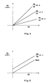
- Fig. 4 is a diagram showing a relationship between the average level VA and the erasing level VE/peak level VP.
- Fig. 5 is a diagram showing a relationship between the average level VA and the bottom level VB/erasing level VE.
- Fig. 1 is a block diagram illustrating an example embodiment of an optical disk recording/reproducing device according to the present invention.
- reference numeral 1 denotes an optical disk placed on a turntable (not shown) rotationally driven by a spindle motor (not shown). The disk is rotated by the rotation of the turntable.
- positional information data is recorded by pregroove.
- the present device is configured such that signal recording/reproducing operation is performed based on a wobble signal obtained from the groove.
- Reference numeral 2 denotes an optical pickup.
- the optical pickup 2 includes a laser element for irradiating a light beam onto the disk 1, and a light detector for receiving a light beam reflected off of a signal recording surface of the disk 1.
- the optical pickup 2 further includes a reflector and a monitor diode. Light irradiated by the laser element is reflected by the reflector, and the reflected light becomes the monitor signal to be irradiated on the monitor diode.
- Reference numeral 3 denotes a pickup feed motor for displacing the optical pickup 2 in the radial direction of the disk 1.
- Numeral 4 denotes a RF signal amplifier circuit for amplifying and performing waveform shaping on a RF signal obtained from the light detector integrated in the optical pickup 2.
- Numeral 5 denotes a pickup control circuit for performing a focusing control to focus a light beam from the optical pickup 2 on the signal surface of the disk 1 based on a signal obtained via the RF signal amplifier circuit 4, and for performing a tracking control to allow the light beam to trace a signal track on the signal surface.
- Numeral 6 denotes a digital signal processing circuit for performing digital signal processing on a signal output from the RF signal amplifier circuit 4, and for demodulating various signals.
- Numeral 7 denotes a signal regenerator circuit which receives input of a digital signal processed by the digital signal processing circuit 6.
- the signal regenerator circuit 7 converts the input signal into an analog signal and outputs the analog signal to an amplifier or the like.
- the signal regenerator circuit 7 outputs the input signal to a computer device in its present from as a digital signal.
- Numeral 8 denotes a manipulation switch unit including switches manipulated for switching among various operations of the optical disk recording/reproducing device.
- Numeral 9 denotes a system control circuit for receiving input of a signal demodulated by the digital processing circuit 6, and for performing various controls according to manipulations of the manipulation switch unit 8.
- Numeral 10 denotes a pickup feed motor driving circuit for driving and controlling the rotation of the pickup feed motor 3. The operation of the pickup feed motor driving circuit 10 is controlled by the system control circuit 9.
- 11 denotes a laser driving circuit for supplying a pulse signal for driving a laser element included in the optical pickup device 2.
- 12 denotes a laser output control circuit, the operation of which is controlled by the system control circuit 9.
- the laser output control circuit 12 controls the laser driving circuit 11 to set the laser output.
- Reference numeral 13 denotes a signal recording circuit for receiving input of a recorded signal of a test signal or a information signal, and for controlling, according to the received signal, the laser irradiating operation of the laser driving circuit 11 to allow recording of a signal on the optical disk 1.
- Reference numeral 14 is a reflected luminous energy detector circuit.
- the reflected luminous energy detector circuit 14 receives input of a monitor signal generated using the monitor diode integrated in the optical pickup 2, and detects the level of the monitor signal to determine the reflected luminous energy level (erasing level VE) of a basic pulse signal as described later. Further, an average level detector circuit 70 provided inside the reflected luminous energy detector circuit 14 detects the average level VA of the monitor signal. The detected values are supplied to the system control circuit 9.
- Reference numeral 15 is a storage unit comprising, for example, a non-volatile memory.
- the storage unit 15 is used especially for storing the average level VA and the erasing level VE of the monitor signal generated when a predetermined basic pulse signal is output in advance to the laser element, as described later.
- the reproducing operation of the optical disk recording/reproducing device having the above-described configuration is next described.
- the system control circuit 9 starts a control for reproduction.
- the device setting is such that the laser element included in the optical pickup 2 is supplied with a drive current from the laser drive circuit 11 to obtain a laser output required for signal readout.
- a spindle motor driving circuit (not shown) performs rotation control of the spindle motor.
- the optical pickup 2 begins the focusing operation and the tracking operation to read out a signal from the disk 1.
- the signal read out by the optical pickup 2 is input to the digital signal processing circuit 6 via the RF signal amplifier circuit 4.
- the digital signal processing circuit 6 executes a signal processing to extract information data. After the information data is processed for error correction and the like, the data is applied to the signal regenerator circuit 7.
- the signal regenerator circuit 7 converts the data into an analog signal and then outputs the analog signal to an amplifier or the like.
- the signal regenerator circuit 7 outputs the input signal to a computer device as is in the form of a digital signal.
- laser output setting operation is first conducted when a disk 1 is inserted in a disk mounting portion to perform signal recording.
- the laser output setting operation is executed by setting the laser output to various output levels according to the basic laser output data stored in advance in a memory circuit (not shown) provided inside the system control circuit 9. Using these laser output levels, test signals are recorded in a trial writing region located on the innermost track side. Each of the recorded test signals is reproduced, and, from among those signals, a signal recorded in the best condition is determined. The laser output used for the determined signal is then designated as the optimal laser output, completing the laser output setting operation. Before or after this laser output setting operation, waveform correction is performed based on the average value VA of the peak and bottom levels of the basic pulse signal (basic laser output data) to adjust the peak level and the bottom level to the optimal levels.
- Fig. 2 is an example configuration of the section which executes the waveform correction of the output pulse signal according to the present invention.
- a pulse signal from the laser driving circuit 11 is supplied to the laser element L1 of the above-described pickup 2, the laser element L1 emits light.
- the monitor diode Dml of the pickup 2 receives the light and generates a current according to the received light intensity.
- This current is supplied as the monitor signal to one of the input terminals of a comparator 52, via a switch SW and a capacitor C in a sample hold unit 50.
- a recording data encoder 90 controls the switch SW to be closed only during the erasing level VE portions of the basic pulse signal.
- the comparator 52 is therefore supplied with only the erasing level VE portions of the monitor signal.
- Supplied to the other input terminal of the comparator 52 is an analog output from a first digital-analog (D/A) converter circuit 60.
- the first D/A converter circuit 60 receives input of digital data corresponding to the erasing level VE portions from the system control circuit 9 of Fig. 1 configured with a microcomputer and other components.
- the first D/A converter circuit 60 then supplies the corresponding analog erasing level VE portions to the comparator 52.
- the comparator 52 compares the erasing level VE of the monitor signal and the erasing level VE according to an instruction from the system control circuit 9, and supplies, to terminal CH1 of the laser driving circuit 11, a current value ie as an erasing level signal for reducing the difference between the two erasing levels VE. In this way, a feedback is provided for the erasing level VE of the basic pulse signal.
- Data corresponding to the peak level VP portions is supplied to the second D/A converter circuit 62 from the system control circuit 9.
- the data is converted into a corresponding analog current value ip in the second D/A converter circuit 62, and output to terminal CH2 of the laser driving circuit 11.
- Data corresponding to the bottom level VB portions is supplied to the third D/A converter circuit 64 from the system control circuit 9.
- the data is converted into a corresponding analog current value ib in the third D/A converter circuit 64, and output to terminal CH3 of the laser driving circuit 11.
- the monitor signal from the monitor diode Dml is supplied to the average level detector circuit 70 provided inside the reflected luminous energy detector circuit 14.
- the detector circuit 70 is configured using a low-pass filter.
- the low-pass filter 70 detects the average level VA of the monitor signal corresponding to the luminous energy generated at the laser element L1. This average level VA is supplied to the system control circuit 9.
- the laser driving circuit 11 receives, via its input channel terminals CH1 ⁇ CH3, the erasing level signal ie, the peak level signal ip, and the bottom level signal ib, respectively.
- terminals EN1, EN2, and EN3 of the laser driving circuit 11 are supplied with outputs from terminals E, P, and B of the recording data encoder 90, respectively.
- the laser driving circuit 11 outputs to the laser element L1 the current signals ie, ip, and ib supplied to the terminals CH1, CH2, and CH3 only when the corresponding outputs E, P, or B supplied to the terminals EN1 ⁇ EN3 are at level H (high).
- the above process will next be described in detail using Fig. 3.
- the basic pulse signal which is generated by the laser driving circuit 11 and output to the laser element L1, has a waveform as shown in Fig. 3(d).
- Output B remains a constant "1" as indicated in Fig. 3(c).
- the laser driving circuit 11 constantly outputs the bottom level signal ib supplied to terminal CH3.
- the bottom level VB of the basic pulse signal is thus determined.
- the erasing level signal ie supplied to terminal CH1 of the laser driving circuit 11 is permitted to be output.
- the current value of "ib+ie” is output to the laser element L1, thereby determining the erasing level VE of the basic pulse signal. Furthermore, referring to Fig. 3(b), the peak level signal ip supplied to terminal CH2 is permitted to be output when output P is "1". During this period, the current value of "ib+ip" is output to the laser element L1, thereby determining the peak level VP of the basic pulse signal.
- each level of the basic pulse signal as shown in Fig. 3(d) is determined according to the output data from the system control circuit 9.
- the system control circuit 9 calculates, based on the "average level VA" of the monitor signal obtained from the average level detector circuit 70, peak level VP and bottom level VB values which should be maintained at a fixed relationship with respect to the erasing level VE detected from the monitor signal. The system control circuit 9 then sets these values in the D/A converter circuits 62 and 64. Through this process without directly sampling the peak level VP, the peak level VP and the bottom level VB of the basic pulse signal used for actual recording can be set at optimal values, allowing adjustment of the waveform of the basic pulse signal to a desired waveform.
- a monitor signal is then obtained from the monitor diode Dm1 which receives the light irradiated from the laser element L1.
- the reflected luminous energy detector circuit 14 detects the average level VA of this monitor signal using the average level detector circuit 70.
- the sample hold unit 50 samples the erasing level VE to perform servo operation, allowing execution of the control for maintaining the erasing level VE at a fixed level.
- Detection of the average level VA is performed while this control is executed.
- the detected average level VA is stored in the non-volatile memory 15. Further, by storing in the non-volatile memory 15 the erasing level VE, peak level VP, and bottom level VB of the basic pulse signal used for the average level detection, waveform correction operation can speedily be executed as described below.
- relationships as shown in Figs. 4 and 5 for example, namely, the relationship in the basic pulse signal between the erasing level VE and the peak level VP and the relationship between the erasing level VE and the bottom level VB, are determined in advance. These relationships are stored in a memory (ROM) inside the system control circuit 9 as a table or relational expressions.
- Fig. 4 shows the relationship between the average level VA and the erasing level VE in monitor signals of the basic pulse signals having different waveforms between VP and VE. More precisely, Fig. 4 illustrates a relationship within a basic pulse signal between the average level VA (LPF output) and the erasing level VE resulting when the direct current bottom level VB component is "0". As shown, the two levels VA and VE are in a proportional relationship, and the slope a is equal to the ratio of the erasing level VE to the peak level VP (VE/VP). Accordingly, even when an identical erasing level VE is detected, the detected average level VA may differ according to the magnitude of the peak level VP with respect to the erasing level VE.
- Fig. 5 shows the relationship between the average level VA and the erasing level VE in monitor signals of the basic pulse signals having different waveforms between VE and VB.
- the bottom level VB component is a direct current component as described above, when the value of the bottom level VB is varied in a monitor signal of a basic pulse signal having the same VP-VE relationship, the average level of the monitor signal is linearly changed.
- the relationship of Fig. 5 is such that the intercept component b increases while the proportional relationship between the detected average level VA and the erasing level VE remains fixed.
- the relationships between the average level VA and the erasing level VE as shown in Figs. 4 and 5 are stored as a table or relational expressions at the time of manufacture of the device in the memory (ROM) integrated within the system control circuit 9.
- setting of laser output is first conducted through recording of a test signal in a trial writing region provided on the innermost track side of the disk. This trial recording is performed using the basic pulse signal employed for the adjustment process at the time of manufacture.
- the average level detector circuit 70 in the reflected luminous energy detector circuit 14 detects an average level VA of the monitor signal obtained from the monitor diode Dml, and the sample hold circuit 50 detects the erasing level VE through sampling.
- data to be set in each of the D/A converter circuits 60,62,64 are determined so as to allow adjustment of the peak level VP, bottom level VB, and erasing level VE of the basic pulse signal to their respective desired values.
- the required power (erasing level) for writing in the trial writing region is 6mW.
- data corresponding to the target erasing level VE value of 6mW is set in the first D/A converter circuit 60, and the laser servo loop performs control to adjust the erasing level VE of the monitor signal to 6mW.
- the bottom level VB is set to 1mW
- the actual erasing level VE becomes 7mW as shown in Fig. 3(d) because of the additional lmW.
- the value of average level VA corresponding to this erasing level VE of 7mW is equal to 7/6 times the average level VA obtained when the erasing level VE is 6mW.
- the value of erasing level VE corresponding to this 7/6 average level VA value (LPF output) can then be calculated.
- the system control circuit 9 calculates data to be output to the third D/A converter circuit 64. This calculated value is temporarily determined as the data to be output to the third D/A converter circuit 64.
- Data to be output to the second D/A converter circuit 62 i.e., the output peak level VP
- the actual average level VA obtained in the average level detector circuit 70 in connection with the monitor signal having the waveform concerned matches the target average level VA value obtained by multiplying 6mW/10mW to the read-out average level value.
- the data which realizes the target average level VA is temporarily determined as the data to be supplied to the second D/A converter circuit 62.
- data to be output to the first D/A converter circuit 60, the second D/A converter circuit 62, and the third D/A converter circuit 64 are temporarily determined.
- a basic pulse signal is generated through timing control as shown in Fig. 3 (a) ⁇ (c), and is output to the laser element L1.
- the average level detector circuit 70 detects the average level VA of the monitor signal obtained from the monitor diode Dm1.
- the system control circuit 9 compares the detected average level VA to a reference average level VA, which is the value obtained by correcting the average level VA stored in advance in the non-volatile memory 15 during manufacture.
- Data to be output to the second D/A converter circuit 62 (i.e., the output peak level VP) is adjusted until the detected average level VA matches the reference average level VA.
- data to be output to the third D/A converter circuit 64 (i.e., the output bottom level VB) is further changed when necessary.
- each of the levels in the output basic pulse signal as shown in Fig. 3(d) is set by the correction processing as described above, and the pulse signal waveform is corrected accordingly.
- the basic pulse signal having the waveform determined by this waveform correction processing is constantly output.
- servo processing is executed to shift the level of the entire waveform-corrected basic pulse signal without changing the relationship among the respective levels in the signal.
- waveform of the pulse signal for recording is corrected based on a table or relational expressions stored in the memory (ROM).
- the average level VA detected during the recording operation matches the average level VA stored in the non-volatile memory 15
- the values of erasing level VE, peak level VP, and bottom level VB stored in the non-volatile memory 15 are used to set the waveform of the pulse signal for recording. Accordingly, in such a case, there is no need to perform the calculation processing for each level, allowing speedup of the waveform correction operation.
- the basic pulse signal output for recording operation in the optical disk recording/reproducing device is not limited to a pulse having a waveform as shown in Fig. 3(d). Rather, in practice, a waveform as shown in Fig. 3(f) is frequently used.
- a level reached by adding ⁇ to "VE+ ⁇ " is used as the initial recording level (i.e., peak level VP), so as to steeply raise the temperature of the recording portion of the disk 1 at the start of recording.
- the peak level VP is "VE+ ⁇ ".
- the ⁇ and ⁇ can be corrected to optimal values, before the start of recording in the actual recording region, through a processing identical to the above waveform correction of the basic pulse signal of Fig. 3(d).
- Addition of ⁇ to "VE+ ⁇ " in the initial peak level of the basic pulse signal can be realized by providing, in the laser output control circuit 11, a terminal CH4 supplied with a current value i ⁇ corresponding to ⁇ , and by controlling this terminal by using the output ⁇ shown in Fig. 3(e) obtained from the recording data encoder 90.
- the value ⁇ can be corrected as follows.
- Stored in the non-volatile memory 15 at the time of manufacture are an average level VA2 detected in a monitor signal of a basic pulse signal having a predetermined amount of ⁇ added, and an average level VA1 detected in a monitor signal of the basic pulse signal without the ⁇ .
- an average level VAd is detected in a monitor signal of the output basic pulse signal.
- Adjustment of the amount of ⁇ to be added can then be executed by referring to this level VAd and the above average levels VA1 and VA2. In this way, a basic pulse signal having a desired power can be adjusted to an optimal value based on the average level VA obtained by detecting each level in that signal.
Landscapes
- Physics & Mathematics (AREA)
- Optics & Photonics (AREA)
- Optical Recording Or Reproduction (AREA)
- Optical Head (AREA)
Abstract
Description
Claims (6)
- An optical disk recording/reproducing device which records a signal on a disk using a laser irradiated from a laser element driven by a pulse signal, whereinan average level of a monitor signal obtained when a basic pulse signal is applied to said laser element is detected,the presently detected average level is compared to a predetermined reference average level of a monitor signal of a reference basic pulse signal, andwaveform of said basic pulse signal is corrected by adjusting a peak level and/or a bottom level of said basic pulse signal such that the detected average level matches said reference average level.
- An optical disk recording/reproducing device as claimed in Claim 1, whereinan average level of said monitor signal of said reference basic pulse signal is obtained and stored in advance of recording, andwhen recording said basic pulse signal in a trial writing region of the optical disk, the average level of the monitor signal of said basic pulse signal is detected, and the detected average level is compared to said average level stored in advance to perform waveform correction of said basic pulse signal.
- An optical disk recording/reproducing device which records a signal on a disk using a laser irradiated from a laser element driven by a pulse signal, comprising:a detector for detecting an average level of a monitor signal obtained when a basic pulse signal is applied to said laser element;a storing unit for storing, in advance, an average level of a monitor signal of a reference basic pulse signal; anda controller for comparing the presently detected average level to a predetermined reference average level corresponding to said stored average level, and for correcting waveform of said basic pulse signal by adjusting a peak level and/or a bottom level of said basic pulse signal to be output such that the detected average level matches said reference average level.
- An optical disk recording/reproducing device as claimed in Claim 3, wherein
said storing unit further stores data concerning a relationship of a peak level and an erasing level with respect to said average level in said basic pulse signal, and data concerning a relationship of the erasing level and a bottom level with respect to said average level. - An optical disk recording/reproducing device as claimed in Claim 3, whereinthe average level obtained from said monitor signal of said reference basic pulse signal is stored in advance in said storing unit, andwhen recording said basic pulse signal in a trial writing region of the optical disk, said detector detects the average level of said monitor signal of said basic pulse signal, andsaid controller compares the detected average level to said average level stored in advance to perform waveform correction of said basic pulse signal.
- An optical disk recording/reproducing device as claimed in Claim 5, wherein
when recording a pulse signal in an actual recording region of said optical disk, an output level of said basic pulse signal after waveform correction is adjusted such that the erasing level of said basic pulse signal is maintained at a predetermined level.
Applications Claiming Priority (2)
| Application Number | Priority Date | Filing Date | Title |
|---|---|---|---|
| JP31382199 | 1999-11-04 | ||
| JP31382199 | 1999-11-04 |
Publications (3)
| Publication Number | Publication Date |
|---|---|
| EP1098305A2 true EP1098305A2 (en) | 2001-05-09 |
| EP1098305A3 EP1098305A3 (en) | 2004-02-04 |
| EP1098305B1 EP1098305B1 (en) | 2006-03-15 |
Family
ID=18045930
Family Applications (1)
| Application Number | Title | Priority Date | Filing Date |
|---|---|---|---|
| EP00309767A Expired - Lifetime EP1098305B1 (en) | 1999-11-04 | 2000-11-03 | Optical disk recording/reproducing device employing waveform correction of laser output signal |
Country Status (5)
| Country | Link |
|---|---|
| US (1) | US6618334B1 (en) |
| EP (1) | EP1098305B1 (en) |
| KR (1) | KR100697173B1 (en) |
| DE (1) | DE60026674T2 (en) |
| TW (1) | TW516029B (en) |
Cited By (2)
| Publication number | Priority date | Publication date | Assignee | Title |
|---|---|---|---|---|
| WO2003071524A3 (en) * | 2002-02-22 | 2004-03-18 | Koninkl Philips Electronics Nv | Methods and devices for recording marks on a recording surface of an optical record carrier and optical record carriers therefor |
| EP1359572A3 (en) * | 2002-05-02 | 2005-05-11 | Pioneer Corporation | Information recording and reproducing apparatus and information recording method |
Families Citing this family (4)
| Publication number | Priority date | Publication date | Assignee | Title |
|---|---|---|---|---|
| JP3613164B2 (en) * | 2000-09-29 | 2005-01-26 | ヤマハ株式会社 | Laser output control device for optical disk recording device |
| JP3768089B2 (en) * | 2000-11-15 | 2006-04-19 | 三洋電機株式会社 | Laser output setting method for optical disc recording / reproducing apparatus |
| JP3830755B2 (en) * | 2000-11-30 | 2006-10-11 | 株式会社リコー | Light quantity control device and information recording device |
| US20050083828A1 (en) * | 2003-10-17 | 2005-04-21 | Chih-Yuan Chen | Apparatus and method for laser power control |
Family Cites Families (8)
| Publication number | Priority date | Publication date | Assignee | Title |
|---|---|---|---|---|
| EP0218449B1 (en) * | 1985-09-30 | 1992-03-04 | Kabushiki Kaisha Toshiba | Apparatus for stabilizing the optical output power of a semiconductor laser |
| US5590111A (en) * | 1990-06-29 | 1996-12-31 | Hitachi, Ltd. | Method of controlling recording of optical records |
| US5412626A (en) * | 1992-03-23 | 1995-05-02 | Matsushita Electric Industrial Co., Ltd. | Method of recording optical information with selective correction in pulse waveform and a recording system therefor |
| JP3089844B2 (en) | 1992-08-25 | 2000-09-18 | ソニー株式会社 | Write-once optical disk recording device |
| JPH08306054A (en) | 1995-04-28 | 1996-11-22 | Sony Corp | Tracking servo circuit |
| JPH0945982A (en) * | 1995-07-26 | 1997-02-14 | Nikon Corp | Laser drive |
| JPH09288840A (en) * | 1996-02-20 | 1997-11-04 | Ricoh Co Ltd | Laser power control device for optical disk drive |
| JPH117645A (en) * | 1997-06-17 | 1999-01-12 | Ricoh Co Ltd | Optical disk drive |
-
2000
- 2000-11-01 US US09/703,563 patent/US6618334B1/en not_active Expired - Fee Related
- 2000-11-03 TW TW089123188A patent/TW516029B/en not_active IP Right Cessation
- 2000-11-03 EP EP00309767A patent/EP1098305B1/en not_active Expired - Lifetime
- 2000-11-03 DE DE60026674T patent/DE60026674T2/en not_active Expired - Lifetime
- 2000-11-03 KR KR1020000065114A patent/KR100697173B1/en not_active Expired - Fee Related
Cited By (2)
| Publication number | Priority date | Publication date | Assignee | Title |
|---|---|---|---|---|
| WO2003071524A3 (en) * | 2002-02-22 | 2004-03-18 | Koninkl Philips Electronics Nv | Methods and devices for recording marks on a recording surface of an optical record carrier and optical record carriers therefor |
| EP1359572A3 (en) * | 2002-05-02 | 2005-05-11 | Pioneer Corporation | Information recording and reproducing apparatus and information recording method |
Also Published As
| Publication number | Publication date |
|---|---|
| US6618334B1 (en) | 2003-09-09 |
| KR20010051419A (en) | 2001-06-25 |
| DE60026674D1 (en) | 2006-05-11 |
| EP1098305A3 (en) | 2004-02-04 |
| TW516029B (en) | 2003-01-01 |
| EP1098305B1 (en) | 2006-03-15 |
| KR100697173B1 (en) | 2007-03-21 |
| DE60026674T2 (en) | 2006-10-19 |
Similar Documents
| Publication | Publication Date | Title |
|---|---|---|
| TW200303532A (en) | Optical disc device | |
| EP1098305B1 (en) | Optical disk recording/reproducing device employing waveform correction of laser output signal | |
| US7298680B2 (en) | Optical disc apparatus | |
| US5539720A (en) | Method and apparatus for driving light source by stored current value and for processing information | |
| US20040079864A1 (en) | High speed sampling circuit | |
| US6990050B2 (en) | Optical disk recording and reproducing apparatus to control the laser power to an optimal value and enable stable recording and reproducing operations | |
| JPH09171631A (en) | Laser power control device for optical disk drive | |
| EP1207524A2 (en) | Laser output circuit for optical disk recording apparatus | |
| EP1213713B1 (en) | Light intensity control and information recording apparatus and method and computer program product | |
| US7577069B2 (en) | Tilt control method and apparatus for optical disc recording and playback apparatus | |
| US8213270B2 (en) | Optical disk recording apparatus and program | |
| JPH10289451A (en) | Optical disk drive | |
| US20040160877A1 (en) | Optical disk apparatus and characteristic determining method | |
| US7626906B2 (en) | Tilt control method and apparatus for optical disc recording and playback apparatus | |
| KR19980026314A (en) | Method and device for controlling light source of optical recording device | |
| JPH10162401A (en) | Optical disc apparatus and method for correcting reference value of emission power of laser diode | |
| JP2003196867A (en) | Tilt adjustment method for optical disk recording / reproducing device | |
| US20030128638A1 (en) | Optical disk device and gain control method used therefor | |
| JP3132691B2 (en) | Optical disk device | |
| JP3552245B2 (en) | Light amount control device and optical disk device | |
| JPH0935434A (en) | Optical disc player | |
| JP2001101661A (en) | Laser output setting method for optical disk recording / reproducing device | |
| JPH11353683A (en) | Laser output setting method for optical disk recording / reproducing device | |
| JP2003242660A (en) | Optical disk apparatus and gain adjustment method thereof | |
| JPH11328709A (en) | Laser output setting method for optical disk recording / reproducing device |
Legal Events
| Date | Code | Title | Description |
|---|---|---|---|
| PUAI | Public reference made under article 153(3) epc to a published international application that has entered the european phase |
Free format text: ORIGINAL CODE: 0009012 |
|
| AK | Designated contracting states |
Kind code of ref document: A2 Designated state(s): AT BE CH CY DE DK ES FI FR GB GR IE IT LI LU MC NL PT SE TR |
|
| AX | Request for extension of the european patent |
Free format text: AL;LT;LV;MK;RO;SI |
|
| PUAL | Search report despatched |
Free format text: ORIGINAL CODE: 0009013 |
|
| AK | Designated contracting states |
Kind code of ref document: A3 Designated state(s): AT BE CH CY DE DK ES FI FR GB GR IE IT LI LU MC NL PT SE TR |
|
| AX | Request for extension of the european patent |
Extension state: AL LT LV MK RO SI |
|
| RIC1 | Information provided on ipc code assigned before grant |
Ipc: 7G 11B 7/125 A Ipc: 7G 11B 7/00 B |
|
| 17P | Request for examination filed |
Effective date: 20040308 |
|
| 17Q | First examination report despatched |
Effective date: 20040429 |
|
| AKX | Designation fees paid |
Designated state(s): DE FR GB |
|
| GRAP | Despatch of communication of intention to grant a patent |
Free format text: ORIGINAL CODE: EPIDOSNIGR1 |
|
| GRAS | Grant fee paid |
Free format text: ORIGINAL CODE: EPIDOSNIGR3 |
|
| GRAA | (expected) grant |
Free format text: ORIGINAL CODE: 0009210 |
|
| AK | Designated contracting states |
Kind code of ref document: B1 Designated state(s): DE FR GB |
|
| REG | Reference to a national code |
Ref country code: GB Ref legal event code: FG4D |
|
| REF | Corresponds to: |
Ref document number: 60026674 Country of ref document: DE Date of ref document: 20060511 Kind code of ref document: P |
|
| RAP2 | Party data changed (patent owner data changed or rights of a patent transferred) |
Owner name: SANYO ELECTRIC CO., LTD. |
|
| ET | Fr: translation filed | ||
| REG | Reference to a national code |
Ref country code: FR Ref legal event code: CA |
|
| PLBE | No opposition filed within time limit |
Free format text: ORIGINAL CODE: 0009261 |
|
| STAA | Information on the status of an ep patent application or granted ep patent |
Free format text: STATUS: NO OPPOSITION FILED WITHIN TIME LIMIT |
|
| 26N | No opposition filed |
Effective date: 20061218 |
|
| PGFP | Annual fee paid to national office [announced via postgrant information from national office to epo] |
Ref country code: DE Payment date: 20101027 Year of fee payment: 11 |
|
| PGFP | Annual fee paid to national office [announced via postgrant information from national office to epo] |
Ref country code: GB Payment date: 20101103 Year of fee payment: 11 |
|
| PGFP | Annual fee paid to national office [announced via postgrant information from national office to epo] |
Ref country code: FR Payment date: 20111118 Year of fee payment: 12 |
|
| GBPC | Gb: european patent ceased through non-payment of renewal fee |
Effective date: 20121103 |
|
| REG | Reference to a national code |
Ref country code: FR Ref legal event code: ST Effective date: 20130731 |
|
| REG | Reference to a national code |
Ref country code: DE Ref legal event code: R119 Ref document number: 60026674 Country of ref document: DE Effective date: 20130601 |
|
| PG25 | Lapsed in a contracting state [announced via postgrant information from national office to epo] |
Ref country code: DE Free format text: LAPSE BECAUSE OF NON-PAYMENT OF DUE FEES Effective date: 20130601 |
|
| PG25 | Lapsed in a contracting state [announced via postgrant information from national office to epo] |
Ref country code: GB Free format text: LAPSE BECAUSE OF NON-PAYMENT OF DUE FEES Effective date: 20121103 Ref country code: FR Free format text: LAPSE BECAUSE OF NON-PAYMENT OF DUE FEES Effective date: 20121130 |