EP1097251B1 - System and method for reducing particles in epitaxial reactors - Google Patents
System and method for reducing particles in epitaxial reactors Download PDFInfo
- Publication number
- EP1097251B1 EP1097251B1 EP99932209A EP99932209A EP1097251B1 EP 1097251 B1 EP1097251 B1 EP 1097251B1 EP 99932209 A EP99932209 A EP 99932209A EP 99932209 A EP99932209 A EP 99932209A EP 1097251 B1 EP1097251 B1 EP 1097251B1
- Authority
- EP
- European Patent Office
- Prior art keywords
- gas
- throttle valve
- chamber
- pressure
- wafer transport
- Prior art date
- Legal status (The legal status is an assumption and is not a legal conclusion. Google has not performed a legal analysis and makes no representation as to the accuracy of the status listed.)
- Expired - Lifetime
Links
- 238000000034 method Methods 0.000 title claims description 25
- 239000002245 particle Substances 0.000 title description 49
- 235000012431 wafers Nutrition 0.000 claims description 128
- 239000004065 semiconductor Substances 0.000 claims description 54
- 238000002955 isolation Methods 0.000 claims description 24
- 230000001105 regulatory effect Effects 0.000 claims description 9
- 230000004044 response Effects 0.000 claims description 6
- 238000011068 loading method Methods 0.000 claims description 3
- 230000001276 controlling effect Effects 0.000 claims 2
- 239000007789 gas Substances 0.000 description 89
- 238000010926 purge Methods 0.000 description 30
- 238000004519 manufacturing process Methods 0.000 description 23
- 230000007547 defect Effects 0.000 description 15
- 230000008569 process Effects 0.000 description 15
- 239000000758 substrate Substances 0.000 description 9
- IJGRMHOSHXDMSA-UHFFFAOYSA-N Atomic nitrogen Chemical compound N#N IJGRMHOSHXDMSA-UHFFFAOYSA-N 0.000 description 7
- XUIMIQQOPSSXEZ-UHFFFAOYSA-N Silicon Chemical compound [Si] XUIMIQQOPSSXEZ-UHFFFAOYSA-N 0.000 description 6
- 238000010586 diagram Methods 0.000 description 6
- 230000000717 retained effect Effects 0.000 description 6
- 229910052710 silicon Inorganic materials 0.000 description 6
- 239000010703 silicon Substances 0.000 description 6
- 238000000151 deposition Methods 0.000 description 5
- 230000008021 deposition Effects 0.000 description 4
- 238000005516 engineering process Methods 0.000 description 4
- 239000000463 material Substances 0.000 description 4
- 230000008030 elimination Effects 0.000 description 3
- 238000003379 elimination reaction Methods 0.000 description 3
- 229910052757 nitrogen Inorganic materials 0.000 description 3
- 238000005229 chemical vapour deposition Methods 0.000 description 2
- 230000001419 dependent effect Effects 0.000 description 2
- 238000005530 etching Methods 0.000 description 2
- 239000012530 fluid Substances 0.000 description 2
- 230000005484 gravity Effects 0.000 description 2
- 238000001459 lithography Methods 0.000 description 2
- 238000012423 maintenance Methods 0.000 description 2
- 238000003756 stirring Methods 0.000 description 2
- 239000000725 suspension Substances 0.000 description 2
- 238000005411 Van der Waals force Methods 0.000 description 1
- 238000009825 accumulation Methods 0.000 description 1
- QVGXLLKOCUKJST-UHFFFAOYSA-N atomic oxygen Chemical compound [O] QVGXLLKOCUKJST-UHFFFAOYSA-N 0.000 description 1
- 230000008901 benefit Effects 0.000 description 1
- 239000012159 carrier gas Substances 0.000 description 1
- 230000008859 change Effects 0.000 description 1
- 238000004140 cleaning Methods 0.000 description 1
- 239000004035 construction material Substances 0.000 description 1
- 238000011109 contamination Methods 0.000 description 1
- 238000000354 decomposition reaction Methods 0.000 description 1
- 229910001873 dinitrogen Inorganic materials 0.000 description 1
- 238000009826 distribution Methods 0.000 description 1
- 230000000694 effects Effects 0.000 description 1
- 238000000407 epitaxy Methods 0.000 description 1
- 230000037406 food intake Effects 0.000 description 1
- 238000010438 heat treatment Methods 0.000 description 1
- 238000007689 inspection Methods 0.000 description 1
- 230000014759 maintenance of location Effects 0.000 description 1
- 230000007246 mechanism Effects 0.000 description 1
- 239000001301 oxygen Substances 0.000 description 1
- 229910052760 oxygen Inorganic materials 0.000 description 1
- 239000013618 particulate matter Substances 0.000 description 1
- 230000035699 permeability Effects 0.000 description 1
- 238000000197 pyrolysis Methods 0.000 description 1
- 230000009467 reduction Effects 0.000 description 1
- 150000003377 silicon compounds Chemical class 0.000 description 1
- 238000012421 spiking Methods 0.000 description 1
- 239000007858 starting material Substances 0.000 description 1
- 230000003068 static effect Effects 0.000 description 1
Images


Classifications
-
- C—CHEMISTRY; METALLURGY
- C30—CRYSTAL GROWTH
- C30B—SINGLE-CRYSTAL GROWTH; UNIDIRECTIONAL SOLIDIFICATION OF EUTECTIC MATERIAL OR UNIDIRECTIONAL DEMIXING OF EUTECTOID MATERIAL; REFINING BY ZONE-MELTING OF MATERIAL; PRODUCTION OF A HOMOGENEOUS POLYCRYSTALLINE MATERIAL WITH DEFINED STRUCTURE; SINGLE CRYSTALS OR HOMOGENEOUS POLYCRYSTALLINE MATERIAL WITH DEFINED STRUCTURE; AFTER-TREATMENT OF SINGLE CRYSTALS OR A HOMOGENEOUS POLYCRYSTALLINE MATERIAL WITH DEFINED STRUCTURE; APPARATUS THEREFOR
- C30B29/00—Single crystals or homogeneous polycrystalline material with defined structure characterised by the material or by their shape
- C30B29/10—Inorganic compounds or compositions
- C30B29/14—Phosphates
-
- C—CHEMISTRY; METALLURGY
- C23—COATING METALLIC MATERIAL; COATING MATERIAL WITH METALLIC MATERIAL; CHEMICAL SURFACE TREATMENT; DIFFUSION TREATMENT OF METALLIC MATERIAL; COATING BY VACUUM EVAPORATION, BY SPUTTERING, BY ION IMPLANTATION OR BY CHEMICAL VAPOUR DEPOSITION, IN GENERAL; INHIBITING CORROSION OF METALLIC MATERIAL OR INCRUSTATION IN GENERAL
- C23C—COATING METALLIC MATERIAL; COATING MATERIAL WITH METALLIC MATERIAL; SURFACE TREATMENT OF METALLIC MATERIAL BY DIFFUSION INTO THE SURFACE, BY CHEMICAL CONVERSION OR SUBSTITUTION; COATING BY VACUUM EVAPORATION, BY SPUTTERING, BY ION IMPLANTATION OR BY CHEMICAL VAPOUR DEPOSITION, IN GENERAL
- C23C16/00—Chemical coating by decomposition of gaseous compounds, without leaving reaction products of surface material in the coating, i.e. chemical vapour deposition [CVD] processes
- C23C16/44—Chemical coating by decomposition of gaseous compounds, without leaving reaction products of surface material in the coating, i.e. chemical vapour deposition [CVD] processes characterised by the method of coating
- C23C16/4401—Means for minimising impurities, e.g. dust, moisture or residual gas, in the reaction chamber
-
- C—CHEMISTRY; METALLURGY
- C23—COATING METALLIC MATERIAL; COATING MATERIAL WITH METALLIC MATERIAL; CHEMICAL SURFACE TREATMENT; DIFFUSION TREATMENT OF METALLIC MATERIAL; COATING BY VACUUM EVAPORATION, BY SPUTTERING, BY ION IMPLANTATION OR BY CHEMICAL VAPOUR DEPOSITION, IN GENERAL; INHIBITING CORROSION OF METALLIC MATERIAL OR INCRUSTATION IN GENERAL
- C23C—COATING METALLIC MATERIAL; COATING MATERIAL WITH METALLIC MATERIAL; SURFACE TREATMENT OF METALLIC MATERIAL BY DIFFUSION INTO THE SURFACE, BY CHEMICAL CONVERSION OR SUBSTITUTION; COATING BY VACUUM EVAPORATION, BY SPUTTERING, BY ION IMPLANTATION OR BY CHEMICAL VAPOUR DEPOSITION, IN GENERAL
- C23C16/00—Chemical coating by decomposition of gaseous compounds, without leaving reaction products of surface material in the coating, i.e. chemical vapour deposition [CVD] processes
- C23C16/44—Chemical coating by decomposition of gaseous compounds, without leaving reaction products of surface material in the coating, i.e. chemical vapour deposition [CVD] processes characterised by the method of coating
- C23C16/4401—Means for minimising impurities, e.g. dust, moisture or residual gas, in the reaction chamber
- C23C16/4408—Means for minimising impurities, e.g. dust, moisture or residual gas, in the reaction chamber by purging residual gases from the reaction chamber or gas lines
-
- C—CHEMISTRY; METALLURGY
- C23—COATING METALLIC MATERIAL; COATING MATERIAL WITH METALLIC MATERIAL; CHEMICAL SURFACE TREATMENT; DIFFUSION TREATMENT OF METALLIC MATERIAL; COATING BY VACUUM EVAPORATION, BY SPUTTERING, BY ION IMPLANTATION OR BY CHEMICAL VAPOUR DEPOSITION, IN GENERAL; INHIBITING CORROSION OF METALLIC MATERIAL OR INCRUSTATION IN GENERAL
- C23C—COATING METALLIC MATERIAL; COATING MATERIAL WITH METALLIC MATERIAL; SURFACE TREATMENT OF METALLIC MATERIAL BY DIFFUSION INTO THE SURFACE, BY CHEMICAL CONVERSION OR SUBSTITUTION; COATING BY VACUUM EVAPORATION, BY SPUTTERING, BY ION IMPLANTATION OR BY CHEMICAL VAPOUR DEPOSITION, IN GENERAL
- C23C16/00—Chemical coating by decomposition of gaseous compounds, without leaving reaction products of surface material in the coating, i.e. chemical vapour deposition [CVD] processes
- C23C16/44—Chemical coating by decomposition of gaseous compounds, without leaving reaction products of surface material in the coating, i.e. chemical vapour deposition [CVD] processes characterised by the method of coating
- C23C16/455—Chemical coating by decomposition of gaseous compounds, without leaving reaction products of surface material in the coating, i.e. chemical vapour deposition [CVD] processes characterised by the method of coating characterised by the method used for introducing gases into reaction chamber or for modifying gas flows in reaction chamber
-
- C—CHEMISTRY; METALLURGY
- C30—CRYSTAL GROWTH
- C30B—SINGLE-CRYSTAL GROWTH; UNIDIRECTIONAL SOLIDIFICATION OF EUTECTIC MATERIAL OR UNIDIRECTIONAL DEMIXING OF EUTECTOID MATERIAL; REFINING BY ZONE-MELTING OF MATERIAL; PRODUCTION OF A HOMOGENEOUS POLYCRYSTALLINE MATERIAL WITH DEFINED STRUCTURE; SINGLE CRYSTALS OR HOMOGENEOUS POLYCRYSTALLINE MATERIAL WITH DEFINED STRUCTURE; AFTER-TREATMENT OF SINGLE CRYSTALS OR A HOMOGENEOUS POLYCRYSTALLINE MATERIAL WITH DEFINED STRUCTURE; APPARATUS THEREFOR
- C30B25/00—Single-crystal growth by chemical reaction of reactive gases, e.g. chemical vapour-deposition growth
- C30B25/02—Epitaxial-layer growth
- C30B25/08—Reaction chambers; Selection of materials therefor
-
- Y—GENERAL TAGGING OF NEW TECHNOLOGICAL DEVELOPMENTS; GENERAL TAGGING OF CROSS-SECTIONAL TECHNOLOGIES SPANNING OVER SEVERAL SECTIONS OF THE IPC; TECHNICAL SUBJECTS COVERED BY FORMER USPC CROSS-REFERENCE ART COLLECTIONS [XRACs] AND DIGESTS
- Y10—TECHNICAL SUBJECTS COVERED BY FORMER USPC
- Y10S—TECHNICAL SUBJECTS COVERED BY FORMER USPC CROSS-REFERENCE ART COLLECTIONS [XRACs] AND DIGESTS
- Y10S414/00—Material or article handling
- Y10S414/135—Associated with semiconductor wafer handling
- Y10S414/139—Associated with semiconductor wafer handling including wafer charging or discharging means for vacuum chamber
Definitions
- the invention relates to the process of forming films of material on semiconductor wafers through the use of carrier gases within a reactor chamber.
- the present invention relates to the epitaxial deposition of specific materials onto a silicon wafer and to a system and method for reducing or eliminating particulate matter and the resulting particle-related defects on the finished wafer.
- the wafers are loaded in one or multiple load locks and transported through a wafer handling chamber to a reactor, where the actual material is deposited onto the semiconductor wafers by means of gases or vapors.
- the gas in the load lock, wafer handling chamber and reactor must be as particle-free as possible in order to reduce the number of defects on the semiconductor wafer surface.
- Epitaxial depositions in general and silicon epitaxial deposition in particular are integral parts of VLSI processing, especially for the advanced bipolar, NMOS and CMOS technologies, since many of the components of the individual transistors and devices are formed in an epitaxial layer.
- the parent substrate is substantially defect-free (the introduction of substantially defect-free silicon wafer starting material in the mid 1970's offered this possibility)
- the growth of defect-free epitaxial layers requires the elimination of particles on the surface of the parent substrate wafer.
- the elimination or substantial decrease in unwanted particles and the associated achievement of very low particle-related defect densities are accomplished by extensive runs and wafer inspection resulting in very low wafer yields.
- particles may enter the semiconductor manufacturing equipment by other means, such as when semiconductor wafers are put into a load lock, during equipment maintenance or through some other indirect source. Particles generated during the process are removed by the laminar flow of the purge gas. The particles may be transported to the inner surfaces of the equipment and adhere thereon. If particles are present in the gas, or suddenly released from the inner surfaces of the equipment, the particles may be transported to the surface of the semiconductor wafer and cause defects. Undesirable particles including the particles that are to be deposited on the semiconductor wafer during the manufacturing process can be attracted to, deposited and retained on the inner surfaces of the semiconductor manufacturing equipment.
- Capillary force is reduced by the reduction of moisture in the equipment.
- the moisture is reduced by use of construction materials with low moisture permeability and the use of a particle and moisture free gas flow through the equipment.
- a dry particle-free gas purge such as dry nitrogen evaporates moisture and purges particles that are only being retained by the capillary force on the inner surfaces of the equipment.
- U.S. Patent Number 5,373,806 to Logar is an example of an attempt to solve the problem of retained particles.
- electrostatic charges are reduced by heating the substrate to a specific temperature lower than the processing temperature prior to production deposition by the use of a radiant source of energy. This is an extra step that must be taken in the manufacturing process; increasing production time and cost.
- particles are removed from the inner surface of the wafer handling chamber and the load locks by purging the wafer handling chamber with a particle-free gas.
- the semiconductor wafers are transported through the wafer handling chamber and load locks.
- a laminar flow of gas is provided so that particles can be picked up and carried with the purge gas through an exhaust outlet located within the wafer handling chamber and load locks.
- the gas flow becomes turbulent, causing particles to be stirred up and transported to the surface of any semiconductor wafer that happen to be in the wafer handling chamber.
- Another problem with the existing system occurs when a gate valve that isolates the wafer handling chamber from the load lock or processing chamber is opened. If there is a pressure difference between the two chamber, the gas flow in one chamber is diverted to the second chamber, which results in turbulence within the both chambers. Because the single stage back pressure regulators do not completely open, particles, vapors and gases back stream from the exhaust outlet into both chambers.
- United States Patent No. 4,747,367 discloses an apparatus for producing a constant flow, constant pressure chemical vapor deposition including a manifold having inlet valves for simultaneously switching equal flows of reactive and nonreactive gas between a process chamber and a vent chamber.
- WO 98/02683 discloses a pneumatically servoed gas pressure regulator providing a wide range of gas flow rates with outlet pressure control.
- the regulator includes a dome loaded gas pressure regulator and a pressure sensor controller integrated in a single unit.
- Japan Patent Application No. 61 272918A discloses a method for making uniform the distribution of reactive gas flow on the surface of a semiconductor wafer wherein a reactive gas exhaust hole is provided both on the outer furnace wall and the inner furnace wall respectively.
- the present invention relates to a method and apparatus for reducing particles in an epitaxial reactor used in processing of semiconductor wafers.
- an apparatus for processing semiconductor wafers comprising: a reactor chamber for processing semiconductor wafers; and a wafer transport chamber having a gas outlet and means for unloading and loading semiconductor wafers from and to the reactor chamber; the apparatus further comprises:
- a method of processing semiconductor wafers in a semiconductor reactor having a wafer transport chamber having a gas outlet and a reactor chamber the method comprises:
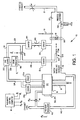
- figure 1 includes a diagram of a piece of semiconductor manufacturing equipment (an epitaxial reactor 10), illustrating a gas purge system 12 that is associated with a wafer transport chamber that includes load locks 14 and 15, and a wafer handling chamber 16.
- the epitaxial reactor 10 is partitioned into the wafer handling chamber 16, load locks 14 and 15, and a process chamber 20 that is isolated from the load locks 14 and 15 and the wafer handling chamber 16 by isolation gate valve 18.
- the load locks 14 and 15 and wafer handling chamber 16 Prior to processing any semiconductor wafers, the load locks 14 and 15 and wafer handling chamber 16 are purged by purge gas from the gas source 22 that includes a control system. This purge gas flows from the source 22 through the pipes 24 and 26 into the load locks 14 and 15 and wafer handling chamber 16.
- cassettes of semiconductor wafers are placed in the load locks 14 and 15 through load lock portals 32 and 34.
- the load lock portals 32 and 34 are closed to isolate the wafers from the surrounding atmosphere.
- the load locks are purged by the purge gas from the gas source 22.
- the purge gas such as dry nitrogen flows through the pipes 24 into the load locks 14 and 15.
- the purge gas purges out oxygen, moisture and undesirable particles that enters the load locks 14 and 15 when the load lock portals 32 and 34 are opened to receive the wafer cassettes.
- the load locks 14 and 15 are opened to the wafer handling chamber by the lowering of the cassette by an elevator 8 which breaks the air tight seal typically located at edge 6, and the wafers are transported sequentially from the cassettes to the process chamber 20 by a transfer arm 29 that has a Bernoulli wan 36 end affecter. While the wafers are transported through the wafer handling chamber 16, the wafer handling chamber 16 is purged by a gas from the gas source 22.
- the purge gas from the gas source is made slightly conductive by passing it through ionizer 21a which is connected to load lock 14, ionizer 21b which is connected to load lock 15, ionizer 21c which is connected to the wafer handling chamber 16 and ionizer 21d which is connected to the Bernoulli wand 36 by a flexible tube 30 that is connected to the robotic arm 29.
- the gas is the same as the purge gas.
- the ionizers 21a, 21b, 21c, and 21d reduces or removes electrostatic forces from inside the epitaxial reactor 10.
- the slightly conductive purge gas can discharge any particles from the wafers or inner surfaces of the chamber subject to the purge.
- the ionizers may be devices such as Model 2201 ss (alpha particle ionizer manufactured by NRD, Inc. of Grand Island, New York or preferably an electronic ionizer, such as the model 4210 manufactured by Ion Systems of Berkeley, California.
- the purge gas flows, under pressure, through the ionizers 21a, 21b, 22c, and 21d.
- the flow rate of the nitrogen purge gas is measured at 15 standard liters per minute (slm), as a Low Flow rate and at 50 slm per minute as a High Flow rate.
- the flow rate is dependent on the volume of chambers and is selected to be as high as possible without creating turbulence.
- a flow rate of 15 slm is common because a higher rate of flow causes turbulence and may stir up and drive particles into suspension with the purge gas.
- a High Flow rate is only used during maintenance mode when there are no wafers in the epitaxial reactor 10, because it stirs up particles and facilitates the cleaning of the equipment.
- the purge gas is slightly conductive, any static in the equipment is reduced or eliminated so that the particles are not attracted to surfaces by electrostatic force, such as the semiconductor wafers (not shown).
- the ionizers 21a, 21 b, 21c and 21d are located as close to the load locks 14 and 15 and the wafer handling chamber 16 as possible. Additionally, there should be no bends in the piping that connects the ionizers 21a 21 b, 21c and 21d to the load locks 14 and 15 and the wafer handling chamber 16.
- the transfer arm 29 is used to move the wafers from the load lock 14 or 15 into the process chamber 20 for wafer processing.
- the transfer arm 29, including a low ingestion Bernoulli wand 36, is within the wafer handling chamber 16.
- the Bernoulli wand 36 picks up the semiconductor wafers one at a time from the cassettes (not shown) in one of the load locks 14 and 15.
- Each wafer is then transported through an open isolation gate valve 18 to a susceptor 38 within the process chamber 20.
- the Bernoulli wand 36 is used to reduce particle accumulation within the epitaxial reactor 10 by avoiding contact with the top and bottom surfaces of the wafers.
- the Bernoulli wand 36 utilizes a novel non-spiking gas system and uses nitrogen gas, through wand gas supply line 28. However, when the Bernoulli wand 36 picks up a wafer and releases it onto the susceptor 38 in the process chamber 20, the resulting impulse of gas released into the wafer handling chamber 16 causes a pressure spike and a resulting turbulence of gas in the wafer handling chamber 16. Any turbulence causes particles that are present within the wafer handling chamber 16 to be disturbed and lifted into suspension in the purging gas. The particles thus can be transported to a wafer surface, however the presence of a damper 44 that dampers the pressure spikes generated from the operation of the Bernoulli wand 36 and prevents the generating of a pressure spike and the resulting turbulence.
- the gas flow is turned off to drop a wafer at its destination, the remaining gas is vented into the wafer handling chamber 16.
- This sudden burst of gas flow causes a sudden pressure rise.
- the damper 44 and orifice 46 is utilized to reduce the pressure spike in the wafer handling chamber 16.
- the dome regulator 90 is shut off and, simultaneously, valve 95 is opened to release the remaining gas flow into the damper 44 and flow resisting orifice 46.
- the size of the damper 44 and the size of the orifice 46 are properly sized, the gas flow increase is gradually released into the wafer handling chamber 16 to compensate for the sudden burst.
- the orifice 46 is sized to provide a tuning mechanism for regulating pressure bursts into the wafer handling chamber 16.
- the damper 44 and orifice 46 is used in conjunction with the back pressure regulator 40 that is located in the exhaust line 42 that is connected to the wafer handling chamber 16.
- the back pressure regulator 40 maintains a constant pressure in the wafer handling chamber 16 and the load locks 14 and 15.
- the valve 41 is opened so that the gas load locks 14 and 15 can be vented.
- the isolation gate valve includes a valve assembly 80 that is constructed to allow the isolation gate valve 18 to open only a minute amount to allow the pressure to equalize between the wafer handling chamber 16 and the process chamber 20.
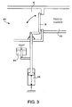
- Figure 3 is a schematic of the isolation gate valve assembly 80.
- the isolation gate valve assembly 80 includes an actuator 82 which is mechanically connected with the isolation gate valve 18, enabling the isolation gate valve 18 to open. Additionally, the isolation gate valve 18 is mechanically connected with a second actuator 84, that actuates the initial opening of the isolation gate valve 18 in a controlled way, allowing the equalization of pressure between the wafer handling chamber 16 and the process chamber 20. The actuator 84 also may control the final closing of the isolation gate valve in a controlled manner.
- This isolation gate valve assembly 80 provides a multispeed isolation gate valve, which can reduce or eliminate gas flow bursts which occur in the initial stage of prior art isolation gate valves.
- the isolation gate valve 18 is opened and the Bernoulli wand 36 retrieves the processed wafer and loads the wafer into a cassette within one of the load locks (14 or 15). After all of the wafers have been processed, the cassette located within the load lock is removed through one of the portals (32 or 34).
- a dome loaded regulator circuit 90 is utilized to feed gas into the semiconductor manufacturing equipment.
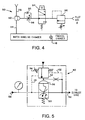
- Figure 4 is a schematic diagram illustrating the dome loaded regulator circuit 90 and includes a dome loaded regulator 92, a valve 94, a pressure regulator 96 and a needle valve 98.
- the gas flow into the equipment is increased incrementally by the dome loaded regulator 92 which is pneumatically actuated by the valve 94, which controls a restricted gas flow.
- the gas flow originates from the pressure regulator 96.
- the needle valve 98 controls the amount of restriction of the gas flow.
- the needle valve 98 may be a plurality of needle valves and check valves, to regulate different ramp-up and ramp-down flow rates of the purge gas.
- FIG. 5 is a schematic diagram of the pilot operated back pressure regulator 40 in the preferred embodiment of the present invention.
- the pilot operated back pressure regulator 40 includes a pneumatically actuated throttle valve 50 which is actuated by a pressure relay system 52.
- the pressure relay system 52 is normally a 22:1 ratio pressure relay that adjusts the opening of the pneumatically actuated throttle valve 50 from the sensed pressure across the throttle valve 50 and conduits 101 and 102.
- the pilot operated back pressure regulator 40 also includes a variable load springs 54 and a throttle valve actuator 56. Additionally, the pilot operated back pressure regulator 40 includes a throttle valve input 58.
- FIG. 6 is a cross sectional side view of the pilot operated back pressure regulator 40 in the preferred embodiment of the present invention.
- the pilot operated back pressure regulator 40 uses the pneumatically actuated throttle valve 50 to regulated the pressure.
- the pilot operated back pressure regulator 40 includes the pressure relay system 52, which is a 22:1 pressure relay in the preferred embodiment, and the pneumatically actuated throttle valve 50.
- the pressure relay system 52 includes a large piston 58 which drives a small pressure reducing regulator 60.
- a high pressure pilot supply 80 PSI in the preferred embodiment
- the variable load spring 54 opens the small pressure regulator 60.
- the opening of the small pressure regulator 60 allows a dynamic flow from a chamber 64 to enter a chamber 68 via a passage 66.
- the dynamic flow then flows through a bleed passage 70 to a passage 72.
- the dynamic flow is exhausted through an output 74 of the pilot operated back pressure regulator 40.
- This dynamic flow creates a bias pressure on the throttle valve actuator 56 at a level just below the pressure required to drive the throttle valve 50 open.
- the size of the bleed passage 70, chamber 68, and a chamber 57 determines the response time and pressure differential necessary to drive the throttle valve 50 open. The smaller the bleed passage 70 and chamber 57, the faster the response of the pilot operated back pressure regulator 40.
- a small increase in pressure at an input 76 for the pilot operated back pressure regulator 40 is transmitted, via a channel 78, to the top of the large piston 58 through the passage 66 driving the small regulator 60 to a higher pressure that is multiplied by the ratio of the pressure relay.
- This increases the pressure at the top of throttle valve actuator 56 and drives the throttle valve 50 open, relieving the pressure at the input 76 of the pilot operated back pressure regulator 40 and thereby regulating the pressure at the throttle valve input 58.
Landscapes
- Chemical & Material Sciences (AREA)
- Engineering & Computer Science (AREA)
- Materials Engineering (AREA)
- Metallurgy (AREA)
- Organic Chemistry (AREA)
- General Chemical & Material Sciences (AREA)
- Chemical Kinetics & Catalysis (AREA)
- Mechanical Engineering (AREA)
- Crystallography & Structural Chemistry (AREA)
- Inorganic Chemistry (AREA)
- Container, Conveyance, Adherence, Positioning, Of Wafer (AREA)
- Chemical Vapour Deposition (AREA)
Description
- The invention relates to the process of forming films of material on semiconductor wafers through the use of carrier gases within a reactor chamber. In particular, the present invention relates to the epitaxial deposition of specific materials onto a silicon wafer and to a system and method for reducing or eliminating particulate matter and the resulting particle-related defects on the finished wafer.
- In most semiconductor manufacturing equipment used for growth of films of material onto semiconductor wafers, the wafers are loaded in one or multiple load locks and transported through a wafer handling chamber to a reactor, where the actual material is deposited onto the semiconductor wafers by means of gases or vapors. The gas in the load lock, wafer handling chamber and reactor must be as particle-free as possible in order to reduce the number of defects on the semiconductor wafer surface.
- Improvements in the capabilities of semiconductor manufacturing equipment continues at an astonishing rate. As capabilities of lithography and etching equipment increases the circuit density on a wafer increases and with the increase in circuit density the specification for particle free environment within the processing equipment also increases. In addition to the resulting circuit density that has been achieved with the improvements in lithography and etching, the size of wafers has increased to 300 mm. Semiconductor manufacturers require further production improvements through the increase in the yields of semiconductor devices from the equipment use to manufacture those devices. The implementation of epitaxial layers, both homoepitaxial and heteroepitaxial, on an underlying substrate layer has a great impact on the yields of the associated semiconductor wafers. A primary example is the growth of epitaxial silicon on a semiconductor wafer substrate. Growth of an epitaxial silicon layer is typically performed in a chemical vapor deposition process in which the wafers are heated while a gaseous silicon compound is passed over the wafer to affect pyrolysis or decomposition. Epitaxial depositions in general and silicon epitaxial deposition in particular are integral parts of VLSI processing, especially for the advanced bipolar, NMOS and CMOS technologies, since many of the components of the individual transistors and devices are formed in an epitaxial layer.
- The ability to process good quality advanced NMOS, CMOS and bipolar IC chips using epitaxy is strongly dependent on maintaining a substantially defect-free state (1) for the bulk semiconductor wafer and for the surface of the bulk wafer, and (2) during the step of depositing the epitaxial silicon layer. Simply put, and as discussed below, elimination of both sub-surface and surface defects is crucial to obtaining good yields in current and future technologies, particularly as those technologies process toward a sub-micron minimum device feature size.
- Surface defects are usually related to undesirable particles. It is extremely critical for sub-micron minimum device feature sizes and for large chip areas that the undesirable particles be eliminated, since a single defect in such devices can cause nonfunctionality of the device and as few as one defect per square centimeter (about 80 defects per four inch wafer) can have catastrophic effects on wafer processing yields. It is a characteristic of epitaxial processing that the crystallographic nature and defect level of the deposited epitaxial layer or epi layer reflects the parent or bulk substrate wafer. Thus, for example, stacking faults on the substrate can give rise to epitaxial stacking faults, and dislocations in the substrate can be transmitted through the epi layer. In addition, epitaxial defects such as pits and micro-contamination result from the bulk substrate wafer surface particles. As a consequence, even where the parent substrate is substantially defect-free (the introduction of substantially defect-free silicon wafer starting material in the mid 1970's offered this possibility), the growth of defect-free epitaxial layers requires the elimination of particles on the surface of the parent substrate wafer. Unfortunately, using present day epitaxial processing technology, the elimination or substantial decrease in unwanted particles and the associated achievement of very low particle-related defect densities are accomplished by extensive runs and wafer inspection resulting in very low wafer yields.
- Although the semiconductor manufacturing equipment is constructed so that particles cannot enter through the walls or with the gas flow, particles may enter the semiconductor manufacturing equipment by other means, such as when semiconductor wafers are put into a load lock, during equipment maintenance or through some other indirect source. Particles generated during the process are removed by the laminar flow of the purge gas. The particles may be transported to the inner surfaces of the equipment and adhere thereon. If particles are present in the gas, or suddenly released from the inner surfaces of the equipment, the particles may be transported to the surface of the semiconductor wafer and cause defects. Undesirable particles including the particles that are to be deposited on the semiconductor wafer during the manufacturing process can be attracted to, deposited and retained on the inner surfaces of the semiconductor manufacturing equipment. Once attracted to the inner surfaces of the semiconductor manufacturing equipment, several different forces including molecular forces (Van der Waals force), capillary forces, and electrostatic forces retain the undesirable particles on the inner surfaces of the semiconductor manufacturing equipment. If for some reason these particles were to be released then they can become airborne and settle on the surfaces of the semiconductor wafers and create defects in the resulting processed wafer. Air turbulence is one way in which these undesirable particles may be freed from their attachment to the inner surfaces of the semiconductor manufacturing equipment.
- Once airborne the movement of particles inside the semiconductor manufacturing equipment is subject to several different forces; gravity, the fluid drag of the surrounding gas flow, and electrostatic force. Gravity is a very weak force on small particles. Normally, a purge with a particle-free gas is maintained through the semiconductor manufacturing equipment in order to create a particle-free environment. Any particles that are released from the inner surfaces of the equipment are transported by the fluid drag of the purge gas to the gas exhaust. However, electrostatic force negatively affects the removal of particles by the purge gas flow. Particles may be transported to semiconductor wafers by the electrostatic force and remain there during the processing of the semiconductor wafer which will result in defects on the surface of the wafers.
- Retention of particles by electrostatic force is erratic since a sudden electrostatic discharge may remove the electrostatic force. The particles released from the inner walls of the equipment may be transported to the surface of a semiconductor wafer and cause defects. Thus it is desirable to eliminate the electrostatic force between particles and the inner walls of the semiconductor manufacturing equipment, so the gas purge flow can remove the retained particles from the inner surfaces of the equipment.
- It takes a large amount of energy to release the particles that are retained on the inner surfaces by molecular force. Therefore particles that are retained by the molecular force on the inner surfaces of the equipment are very likely to stay there indefinitely and not cause any defects on semiconductor wafers.
- Capillary force is reduced by the reduction of moisture in the equipment. The moisture is reduced by use of construction materials with low moisture permeability and the use of a particle and moisture free gas flow through the equipment. A dry particle-free gas purge such as dry nitrogen evaporates moisture and purges particles that are only being retained by the capillary force on the inner surfaces of the equipment.
-
U.S. Patent Number 5,373,806 to Logar (Logar) is an example of an attempt to solve the problem of retained particles. In Logar, electrostatic charges are reduced by heating the substrate to a specific temperature lower than the processing temperature prior to production deposition by the use of a radiant source of energy. This is an extra step that must be taken in the manufacturing process; increasing production time and cost. - Typically particles are removed from the inner surface of the wafer handling chamber and the load locks by purging the wafer handling chamber with a particle-free gas. The semiconductor wafers are transported through the wafer handling chamber and load locks. A laminar flow of gas is provided so that particles can be picked up and carried with the purge gas through an exhaust outlet located within the wafer handling chamber and load locks. However, when a sudden pressure or flow change occurs, the gas flow becomes turbulent, causing particles to be stirred up and transported to the surface of any semiconductor wafer that happen to be in the wafer handling chamber.
- Existing systems used to regulate the pressure inside the semiconductor manufacturing equipment often employ the use of a single stage back pressure regulator that is located between a processing chamber and an exhaust outlet. However, the single stage back pressure regulator has difficulty regulating pressure for a large flow of gas.
- Another problem with the existing system occurs when a gate valve that isolates the wafer handling chamber from the load lock or processing chamber is opened. If there is a pressure difference between the two chamber, the gas flow in one chamber is diverted to the second chamber, which results in turbulence within the both chambers. Because the single stage back pressure regulators do not completely open, particles, vapors and gases back stream from the exhaust outlet into both chambers.
- Thus, it would be a distinct advantage to have an apparatus and method for reducing particles in a epitaxial reactor during the processing of semiconductor wafers. It is an aim of the present invention to provide such an apparatus and method.
- International Patent Application
WO 97/14179 - United States Patent No.
4,747,367 discloses an apparatus for producing a constant flow, constant pressure chemical vapor deposition including a manifold having inlet valves for simultaneously switching equal flows of reactive and nonreactive gas between a process chamber and a vent chamber. - International Patent Application
WO 98/02683 - Japan Patent Application No.
61 272918A - The present invention relates to a method and apparatus for reducing particles in an epitaxial reactor used in processing of semiconductor wafers.
- According to one aspect of the present invention we provide an apparatus for processing semiconductor wafers, comprising: a reactor chamber for processing semiconductor wafers; and a wafer transport chamber having a gas outlet and means for unloading and loading semiconductor wafers from and to the reactor chamber;
the apparatus further comprises: - a gas delivery system operatively connected to deliver gas to the wafer transport chamber, and
- a pilot operated back pressure regulator connected to the gas outlet for regulating the gas pressure in the wafer transport chamber,
- a pneumatically driven throttle valve having an adjustable valve opening connected to the gas outlet;
- a throttle valve actuator for opening the throttle valve; and
- a pressure sensing relay system connected to sense the pressure differential across the pneumatically driven throttle valve and to adjust the adjustable valve opening in response to the sensed pressure differential, the relay system including a pilot gas passage that receives a pilot gas to allow a dynamic flow to create a bias pressure on the throttle valve actuator which drives open the throttle valve.
- According to another aspect of the present invention we provide a method of processing semiconductor wafers in a semiconductor reactor having a wafer transport chamber having a gas outlet and a reactor chamber, the method comprises:
- delivering a gas to the wafer transport chamber;
- regulating the gas pressure in the wafer transport chamber a pilot operated back pressure regulator operatively connected to the gas outlet,
- a pneumatically driven throttle valve having an adjustable valve opening connected to the gas outlet; and
- a throttle valve actuator for opening the throttle valve;
- using a pressure sensing relay system to sense a pressure differential across the throttle valve and to adjust the adjustable valve opening in response to the sensed pressure differential; and
- exposing the regulator to a pilot gas from a pilot gas passage so that a dynamic flow of the pilot gas creates a bias pressure on the throttle valve actuator, which drives open the throttle valve.
-
-
Figure 1 is a diagram of the semiconductor manufacturing equipment, showing gas purge lines that are associated with the load locks and the wafer handling chamber according to the teachings of the present invention: -
Figure 2 is a perspective view of the semiconductor manufacturing equipment illustrating the load locks, the wafer handling chamber and an epitaxial reactor; -
Figure 3 is a schematic of an isolation valve assembly in the preferred embodiment of the present invention; -
Figure 4 is a schematic diagram illustrating the dome loaded regulator circuit in a preferred embodiment of the present invention; -
Figure 5 is a schematic diagram of the pilot operated back pressure regulator in the preferred embodiment of the present invention; and, -
Figure 6 is a cross sectional side view of the pilot operated back pressure regulator in the preferred embodiment of the present invention. - Referring to
figures 1 and2 whereinfigure 1 includes a diagram of a piece of semiconductor manufacturing equipment (an epitaxial reactor 10), illustrating agas purge system 12 that is associated with a wafer transport chamber that includes load locks 14 and 15, and awafer handling chamber 16. Theepitaxial reactor 10 is partitioned into thewafer handling chamber 16, load locks 14 and 15, and aprocess chamber 20 that is isolated from the load locks 14 and 15 and thewafer handling chamber 16 byisolation gate valve 18. - Prior to processing any semiconductor wafers, the load locks 14 and 15 and
wafer handling chamber 16 are purged by purge gas from thegas source 22 that includes a control system. This purge gas flows from thesource 22 through thepipes wafer handling chamber 16. - In operation, cassettes of semiconductor wafers (not shown) are placed in the load locks 14 and 15 through
load lock portals load lock portals gas source 22. The purge gas such as dry nitrogen flows through thepipes 24 into the load locks 14 and 15. The purge gas purges out oxygen, moisture and undesirable particles that enters the load locks 14 and 15 when theload lock portals - After completing the purge, the load locks 14 and 15 are opened to the wafer handling chamber by the lowering of the cassette by an
elevator 8 which breaks the air tight seal typically located atedge 6, and the wafers are transported sequentially from the cassettes to theprocess chamber 20 by atransfer arm 29 that has aBernoulli wan 36 end affecter. While the wafers are transported through thewafer handling chamber 16, thewafer handling chamber 16 is purged by a gas from thegas source 22. - The purge gas from the gas source is made slightly conductive by passing it through ionizer 21a which is connected to load
lock 14,ionizer 21b which is connected to loadlock 15,ionizer 21c which is connected to thewafer handling chamber 16 and ionizer 21d which is connected to theBernoulli wand 36 by aflexible tube 30 that is connected to therobotic arm 29. InFigure 1 , the gas is the same as the purge gas. Theionizers epitaxial reactor 10. The slightly conductive purge gas can discharge any particles from the wafers or inner surfaces of the chamber subject to the purge. - The ionizers may be devices such as Model 2201 ss (alpha particle ionizer manufactured by NRD, Inc. of Grand Island, New York or preferably an electronic ionizer, such as the model 4210 manufactured by Ion Systems of Berkeley, California.
- The purge gas flows, under pressure, through the
ionizers 21a, 21b, 22c, and 21d. the flow rate of the nitrogen purge gas is measured at 15 standard liters per minute (slm), as a Low Flow rate and at 50 slm per minute as a High Flow rate. The flow rate is dependent on the volume of chambers and is selected to be as high as possible without creating turbulence. - A flow rate of 15 slm is common because a higher rate of flow causes turbulence and may stir up and drive particles into suspension with the purge gas. A High Flow rate is only used during maintenance mode when there are no wafers in the
epitaxial reactor 10, because it stirs up particles and facilitates the cleaning of the equipment. However, when the purge gas is slightly conductive, any static in the equipment is reduced or eliminated so that the particles are not attracted to surfaces by electrostatic force, such as the semiconductor wafers (not shown). - Preferably, the
ionizers wafer handling chamber 16 as possible. Additionally, there should be no bends in the piping that connects theionizers 21a wafer handling chamber 16. - Subsequent to the purging of the load locks 14 and 15 and
wafer handling chamber 16, theisolation valve 18 is opened. Thetransfer arm 29 is used to move the wafers from theload lock process chamber 20 for wafer processing. Thetransfer arm 29, including a lowingestion Bernoulli wand 36, is within thewafer handling chamber 16. In operation, theBernoulli wand 36 picks up the semiconductor wafers one at a time from the cassettes (not shown) in one of the load locks 14 and 15. Each wafer is then transported through an openisolation gate valve 18 to asusceptor 38 within theprocess chamber 20. TheBernoulli wand 36 is used to reduce particle accumulation within theepitaxial reactor 10 by avoiding contact with the top and bottom surfaces of the wafers. TheBernoulli wand 36 utilizes a novel non-spiking gas system and uses nitrogen gas, through wandgas supply line 28. However, when theBernoulli wand 36 picks up a wafer and releases it onto thesusceptor 38 in theprocess chamber 20, the resulting impulse of gas released into thewafer handling chamber 16 causes a pressure spike and a resulting turbulence of gas in thewafer handling chamber 16. Any turbulence causes particles that are present within thewafer handling chamber 16 to be disturbed and lifted into suspension in the purging gas. The particles thus can be transported to a wafer surface, however the presence of adamper 44 that dampers the pressure spikes generated from the operation of theBernoulli wand 36 and prevents the generating of a pressure spike and the resulting turbulence. - When using a
Bernoulli wand 36, the gas flow is turned off to drop a wafer at its destination, the remaining gas is vented into thewafer handling chamber 16. This sudden burst of gas flow causes a sudden pressure rise. In order to render the gas flow constant, thedamper 44 andorifice 46 is utilized to reduce the pressure spike in thewafer handling chamber 16. When a wafer is released, thedome regulator 90 is shut off and, simultaneously,valve 95 is opened to release the remaining gas flow into thedamper 44 andflow resisting orifice 46. When the size of thedamper 44 and the size of theorifice 46 are properly sized, the gas flow increase is gradually released into thewafer handling chamber 16 to compensate for the sudden burst. Theorifice 46 is sized to provide a tuning mechanism for regulating pressure bursts into thewafer handling chamber 16. - The
damper 44 andorifice 46 is used in conjunction with theback pressure regulator 40 that is located in theexhaust line 42 that is connected to thewafer handling chamber 16. Theback pressure regulator 40 maintains a constant pressure in thewafer handling chamber 16 and the load locks 14 and 15. When theelevator 8 is sealently pressed against theedge 6, thevalve 41 is opened so that the gas load locks 14 and 15 can be vented. - Another area in which the gas flow is disturbed occurs when the
isolation gate valve 18 is suddenly opened or closed when transporting wafers between thewafer handling chamber 16 and theprocess chamber 20. In order to minimize this gas flow disturbance, the isolation gate valve includes avalve assembly 80 that is constructed to allow theisolation gate valve 18 to open only a minute amount to allow the pressure to equalize between thewafer handling chamber 16 and theprocess chamber 20.Figure 3 is a schematic of the isolationgate valve assembly 80. Once the pressure is equalized between thewafer handling chamber 16 and theprocess chamber 20, theisolation gate valve 18 continues to open at a fast rate. This results in a minimum disturbance in pressure and gas flow while still allowing fast actuation of theisolation gate valve 18. - The isolation
gate valve assembly 80 includes anactuator 82 which is mechanically connected with theisolation gate valve 18, enabling theisolation gate valve 18 to open. Additionally, theisolation gate valve 18 is mechanically connected with asecond actuator 84, that actuates the initial opening of theisolation gate valve 18 in a controlled way, allowing the equalization of pressure between thewafer handling chamber 16 and theprocess chamber 20. Theactuator 84 also may control the final closing of the isolation gate valve in a controlled manner. This isolationgate valve assembly 80 provides a multispeed isolation gate valve, which can reduce or eliminate gas flow bursts which occur in the initial stage of prior art isolation gate valves. - After each wafer is processed, the
isolation gate valve 18 is opened and theBernoulli wand 36 retrieves the processed wafer and loads the wafer into a cassette within one of the load locks (14 or 15). After all of the wafers have been processed, the cassette located within the load lock is removed through one of the portals (32 or 34). - Disturbance of the flow and pressure of the purge gas may also occur during the sudden opening or closing of gas valves which feeds gas into the semiconductor manufacturing equipment. A dome loaded
regulator circuit 90 is utilized to feed gas into the semiconductor manufacturing equipment.Figure 4 is a schematic diagram illustrating the dome loadedregulator circuit 90 and includes a dome loadedregulator 92, avalve 94, apressure regulator 96 and aneedle valve 98. The gas flow into the equipment is increased incrementally by the dome loadedregulator 92 which is pneumatically actuated by thevalve 94, which controls a restricted gas flow. The gas flow originates from thepressure regulator 96. In addition, theneedle valve 98 controls the amount of restriction of the gas flow. However, theneedle valve 98 may be a plurality of needle valves and check valves, to regulate different ramp-up and ramp-down flow rates of the purge gas. -
Figure 5 is a schematic diagram of the pilot operatedback pressure regulator 40 in the preferred embodiment of the present invention. The pilot operatedback pressure regulator 40 includes a pneumatically actuatedthrottle valve 50 which is actuated by apressure relay system 52. Thepressure relay system 52 is normally a 22:1 ratio pressure relay that adjusts the opening of the pneumatically actuatedthrottle valve 50 from the sensed pressure across thethrottle valve 50 andconduits back pressure regulator 40 also includes a variable load springs 54 and athrottle valve actuator 56. Additionally, the pilot operatedback pressure regulator 40 includes athrottle valve input 58. -
Figure 6 is a cross sectional side view of the pilot operatedback pressure regulator 40 in the preferred embodiment of the present invention. Referring toFigure 6 , the operation of the pilot operatedback pressure regulator 40 will now be explained. In order to regulate the pressure within thewafer handling chamber 16, the pilot operatedback pressure regulator 40 uses the pneumatically actuatedthrottle valve 50 to regulated the pressure. The pilot operatedback pressure regulator 40 includes thepressure relay system 52, which is a 22:1 pressure relay in the preferred embodiment, and the pneumatically actuatedthrottle valve 50. Thepressure relay system 52 includes alarge piston 58 which drives a smallpressure reducing regulator 60. A high pressure pilot supply (80 PSI in the preferred embodiment), is feed in through apassage 62. Thevariable load spring 54 opens thesmall pressure regulator 60. The opening of thesmall pressure regulator 60 allows a dynamic flow from achamber 64 to enter achamber 68 via apassage 66. The dynamic flow then flows through ableed passage 70 to apassage 72. From thepassage 72, the dynamic flow is exhausted through anoutput 74 of the pilot operatedback pressure regulator 40. This dynamic flow creates a bias pressure on thethrottle valve actuator 56 at a level just below the pressure required to drive thethrottle valve 50 open. The size of thebleed passage 70,chamber 68, and achamber 57 determines the response time and pressure differential necessary to drive thethrottle valve 50 open. The smaller thebleed passage 70 andchamber 57, the faster the response of the pilot operatedback pressure regulator 40. A small increase in pressure at aninput 76 for the pilot operatedback pressure regulator 40 is transmitted, via achannel 78, to the top of thelarge piston 58 through thepassage 66 driving thesmall regulator 60 to a higher pressure that is multiplied by the ratio of the pressure relay. This increases the pressure at the top ofthrottle valve actuator 56 and drives thethrottle valve 50 open, relieving the pressure at theinput 76 of the pilot operatedback pressure regulator 40 and thereby regulating the pressure at thethrottle valve input 58.
Claims (8)
- An apparatus for processing semiconductor wafers, comprising: a reactor chamber (20) for processing semiconductor wafers; and a wafer transport chamber (16) having a gas outlet and means (29, 30) for unloading and loading semiconductor wafers from and to the reactor chamber (20);
the apparatus further comprises:a gas delivery system operatively connected to deliver gas to the wafer transport chamber (16); anda pilot operated back pressure regulator (40) connected to the gas outlet for regulating the gas pressure in the wafer transport chamber (16),characterized in that the regulator (40) includes:a pneumatically driven throttle valve (50) having an adjustable valve opening connected to the gas outlet;a throttle valve actuator (56) for opening the throttle valve (50); anda pressure sensing relay system (52) connected to sense the pressure differential across the pneumatically driven throttle valve (50) and to adjust the adjustable valve opening in response to the sensed pressure differential, the relay system including a pilot gas passage (62) that receives a pilot gas to allow a dynamic flow to create a bias pressure on the throttle valve actuator (56) which drives open the throttle valve (50). - The apparatus of Claim 1 wherein the gas delivery system includes at least a gas source (22) and a first line (28) connecting the gas source (22) to the wafer transport chamber (16), the apparatus further comprising: a dome loaded regulator (90) integrally connected to the gas delivery system in the first line (28) for regulating the delivery of gas to the wafer transport chamber (16).
- The apparatus according to Claim 2 wherein the gas delivery system further includes a second line (26) connecting the gas source (22) to the wafer transport chamber (16), the apparatus further comprising: a damper (44) connected in line with the gas delivery system in the second line (26); and a gas flow restricting means (46) located in line between the damper (44) and the wafer transport chamber (16).
- The apparatus according to Claims 2 or 3 further comprising: an isolation valve (18) located between the reactor chamber (20) and the wafer transport chamber (16); and means (82, 84) for controlling opening of the isolation valve (18) at a first speed followed by a second speed.
- The apparatus according to Claim 1 wherein the gas delivery system includes at least a gas source (22) and a first line (26) connecting the gas source (22) to the wafer transport chamber (16), the apparatus further comprising: a damper (44) connected in line with the gas delivery system in the first line (26); and a gas flow restricting means (46) located in line between the damper (44) and the wafer transport chamber (16).
- The apparatus according to Claim 1 further comprising: an isolation valve (18) located between the reactor chamber (20) and the wafer transport chamber (16); and means (82, 84) for controlling opening of the isolation valve (18) at a first speed followed by a second speed.
- The apparatus according to Claim 1, wherein the pressure sensing relay system (52) includes a piston (58) and a small pressure reducing regulator (60) connected to the piston (58), the piston (58) exposed to the pressure differential across the throttle valve (50), the apparatus further including:a variable load spring (54) pushing the piston (58) and small pressure reducing regulator (60) in a direction that opens a path between the pilot gas passage (62) and a chamber (68); anda throttle valve actuator (56) connected to the throttle valve (50) and exposed to the chamber (68), so that gas pressure in the chamber (68) causes the throttle valve actuator (56) to move the throttle valve (50) and thereby adjust the adjustable valve opening of the throttle valve (50).
- A method of processing semiconductor wafers in a semiconductor reactor (10) having a wafer transport chamber (16) having a gas outlet and a reactor chamber (20), the method comprises:delivering a gas to the wafer transport chamber (16);regulating the gas pressure in the wafer transport chamber (16) with a pilot operated back pressure regulator (40) operatively connected to the gas outlet,characterized in that the regulator includes:a pneumatically driven throttle valve (50) having an adjustable valve opening connected to the gas outlet; anda throttle valve actuator (56) for opening the throttle valve (50);using a pressure sensing relay system (52) to sense a pressure differential across the throttle valve (50) and to adjust the adjustable valve opening in response to the sensed pressure differential; andexposing the regulator (40) to a pilot gas from a pilot gas passage (62) so that a dynamic flow of the pilot gas creates a bias pressure on the throttle valve actuator (56), which drives open the throttle valve (50).
Priority Applications (1)
| Application Number | Priority Date | Filing Date | Title |
|---|---|---|---|
| EP08006163A EP1956112A3 (en) | 1998-07-10 | 1999-06-30 | System and method for reducing particles in epitaxial reactors |
Applications Claiming Priority (3)
| Application Number | Priority Date | Filing Date | Title |
|---|---|---|---|
| US113934 | 1993-08-30 | ||
| US09/113,934 US6161311A (en) | 1998-07-10 | 1998-07-10 | System and method for reducing particles in epitaxial reactors |
| PCT/US1999/015070 WO2000003056A1 (en) | 1998-07-10 | 1999-06-30 | System and method for reducing particles in epitaxial reactors |
Related Child Applications (1)
| Application Number | Title | Priority Date | Filing Date |
|---|---|---|---|
| EP08006163A Division EP1956112A3 (en) | 1998-07-10 | 1999-06-30 | System and method for reducing particles in epitaxial reactors |
Publications (3)
| Publication Number | Publication Date |
|---|---|
| EP1097251A1 EP1097251A1 (en) | 2001-05-09 |
| EP1097251A4 EP1097251A4 (en) | 2005-01-12 |
| EP1097251B1 true EP1097251B1 (en) | 2008-12-10 |
Family
ID=22352390
Family Applications (2)
| Application Number | Title | Priority Date | Filing Date |
|---|---|---|---|
| EP08006163A Withdrawn EP1956112A3 (en) | 1998-07-10 | 1999-06-30 | System and method for reducing particles in epitaxial reactors |
| EP99932209A Expired - Lifetime EP1097251B1 (en) | 1998-07-10 | 1999-06-30 | System and method for reducing particles in epitaxial reactors |
Family Applications Before (1)
| Application Number | Title | Priority Date | Filing Date |
|---|---|---|---|
| EP08006163A Withdrawn EP1956112A3 (en) | 1998-07-10 | 1999-06-30 | System and method for reducing particles in epitaxial reactors |
Country Status (7)
| Country | Link |
|---|---|
| US (2) | US6161311A (en) |
| EP (2) | EP1956112A3 (en) |
| JP (1) | JP2002520832A (en) |
| KR (1) | KR20010071820A (en) |
| DE (1) | DE69940064D1 (en) |
| TW (1) | TW445304B (en) |
| WO (1) | WO2000003056A1 (en) |
Families Citing this family (41)
| Publication number | Priority date | Publication date | Assignee | Title |
|---|---|---|---|---|
| US6153044A (en) * | 1998-04-30 | 2000-11-28 | Euv Llc | Protection of lithographic components from particle contamination |
| TW513617B (en) * | 1999-04-21 | 2002-12-11 | Asml Corp | Lithographic projection apparatus and method of manufacturing a device using a lithographic projection apparatus |
| TW472296B (en) * | 1999-05-25 | 2002-01-11 | Ebara Corp | Substrate treating apparatus and method of operating the same |
| US6279249B1 (en) | 1999-12-30 | 2001-08-28 | Intel Corporation | Reduced particle contamination manufacturing and packaging for reticles |
| JP3955724B2 (en) * | 2000-10-12 | 2007-08-08 | 株式会社ルネサステクノロジ | Manufacturing method of semiconductor integrated circuit device |
| JP4916070B2 (en) * | 2001-09-26 | 2012-04-11 | アプライド マテリアルズ インコーポレイテッド | Substrate processing equipment |
| JP2003109994A (en) * | 2001-09-26 | 2003-04-11 | Applied Materials Inc | Substrate processing equipment |
| DE10203833B4 (en) * | 2002-01-31 | 2007-02-08 | Siltronic Ag | Method and device for differential pressure control on epitaxy reactors |
| JP4531557B2 (en) * | 2002-05-21 | 2010-08-25 | エーエスエム アメリカ インコーポレイテッド | Reduction of cross-contamination between chambers in semiconductor processing tools |
| DE10247051A1 (en) * | 2002-10-09 | 2004-04-22 | Polymer Latex Gmbh & Co Kg | Latex and process for its manufacture |
| US7100954B2 (en) * | 2003-07-11 | 2006-09-05 | Nexx Systems, Inc. | Ultra-thin wafer handling system |
| KR101027825B1 (en) * | 2003-09-11 | 2011-04-07 | 파나소닉 주식회사 | Vision processing device, vision processing method, vision processing program and semiconductor device |
| US8608422B2 (en) * | 2003-10-08 | 2013-12-17 | Tokyo Electron Limited | Particle sticking prevention apparatus and plasma processing apparatus |
| DE20321795U1 (en) * | 2003-12-11 | 2010-03-04 | Voith Patent Gmbh | Apparatus for cleaning at least one process chamber for coating at least one substrate |
| US7416370B2 (en) * | 2005-06-15 | 2008-08-26 | Lam Research Corporation | Method and apparatus for transporting a substrate using non-Newtonian fluid |
| US20060174835A1 (en) * | 2005-02-10 | 2006-08-10 | Misako Saito | Vacuum processing apparatus and method of using the same |
| KR100745966B1 (en) * | 2005-12-29 | 2007-08-02 | 동부일렉트로닉스 주식회사 | Plasma treatment apparatus and cleaning method thereof |
| US20080067368A1 (en) * | 2006-04-19 | 2008-03-20 | Mks Instruments Inc | Ionizing system for vacuum process and metrology equipment |
| KR100774711B1 (en) * | 2006-07-19 | 2007-11-08 | 동부일렉트로닉스 주식회사 | Particle removal device and method for removing epitaxial equipment for semiconductor manufacturing |
| US7972961B2 (en) * | 2008-10-09 | 2011-07-05 | Asm Japan K.K. | Purge step-controlled sequence of processing semiconductor wafers |
| US20100119351A1 (en) * | 2008-11-13 | 2010-05-13 | Wafertech, Llc | Method and system for venting load lock chamber to a desired pressure |
| US8216380B2 (en) * | 2009-01-08 | 2012-07-10 | Asm America, Inc. | Gap maintenance for opening to process chamber |
| US8287648B2 (en) | 2009-02-09 | 2012-10-16 | Asm America, Inc. | Method and apparatus for minimizing contamination in semiconductor processing chamber |
| JP5439097B2 (en) * | 2009-09-08 | 2014-03-12 | 東京応化工業株式会社 | Coating apparatus and coating method |
| JP5639816B2 (en) * | 2009-09-08 | 2014-12-10 | 東京応化工業株式会社 | Coating method and coating apparatus |
| JP5719546B2 (en) * | 2009-09-08 | 2015-05-20 | 東京応化工業株式会社 | Coating apparatus and coating method |
| JP5469966B2 (en) * | 2009-09-08 | 2014-04-16 | 東京応化工業株式会社 | Coating apparatus and coating method |
| US8416552B2 (en) * | 2009-10-23 | 2013-04-09 | Illinois Tool Works Inc. | Self-balancing ionized gas streams |
| JP2013531899A (en) * | 2010-07-02 | 2013-08-08 | マシスン トライ−ガス インコーポレイテッド | Selective epitaxy of SI-containing materials and substitutionally doped crystalline SI-containing materials |
| US9031700B2 (en) | 2011-10-11 | 2015-05-12 | Intermolecular, Inc. | Facilities manifold with proximity sensor |
| US9082608B2 (en) | 2012-12-03 | 2015-07-14 | Intermolecular, Inc. | Pneumatic clamping mechanism for cells with adjustable height |
| US9269567B2 (en) | 2013-12-17 | 2016-02-23 | Intermolecular, Inc. | High productivity combinatorial processing using pressure-controlled one-way valves |
| KR20180071360A (en) * | 2015-10-25 | 2018-06-27 | 어플라이드 머티어리얼스, 인코포레이티드 | Apparatus for vacuum deposition on a substrate and method for masking a substrate during vacuum deposition |
| CN106876299B (en) * | 2015-12-11 | 2019-08-23 | 北京北方华创微电子装备有限公司 | Semiconductor processing equipment |
| CN107761165A (en) * | 2016-08-15 | 2018-03-06 | 上海新昇半导体科技有限公司 | A kind of base and epitaxial device based on Bernoulli effect |
| US10872804B2 (en) | 2017-11-03 | 2020-12-22 | Asm Ip Holding B.V. | Apparatus and methods for isolating a reaction chamber from a loading chamber resulting in reduced contamination |
| US10872803B2 (en) | 2017-11-03 | 2020-12-22 | Asm Ip Holding B.V. | Apparatus and methods for isolating a reaction chamber from a loading chamber resulting in reduced contamination |
| TWI890811B (en) * | 2020-06-17 | 2025-07-21 | 美商應用材料股份有限公司 | Process chamber lid and processing method for high temperature chemical vapor deposition |
| KR102858574B1 (en) * | 2021-08-06 | 2025-09-11 | 세메스 주식회사 | Method for stabilizing particles |
| US11864299B2 (en) * | 2022-05-10 | 2024-01-02 | Applied Materials, Inc. | System and method for dissipating workpiece charge build up |
| US12460863B2 (en) * | 2022-05-26 | 2025-11-04 | Semes Co., Ltd. | Apparatus for treating a substrate |
Family Cites Families (36)
| Publication number | Priority date | Publication date | Assignee | Title |
|---|---|---|---|---|
| JPS59222922A (en) * | 1983-06-01 | 1984-12-14 | Nippon Telegr & Teleph Corp <Ntt> | Vapor growth apparatus |
| US5373806A (en) * | 1985-05-20 | 1994-12-20 | Applied Materials, Inc. | Particulate-free epitaxial process |
| JPS61272918A (en) * | 1985-05-29 | 1986-12-03 | Hitachi Electronics Eng Co Ltd | Cvd device improving gas flow distribution |
| US4747367A (en) * | 1986-06-12 | 1988-05-31 | Crystal Specialties, Inc. | Method and apparatus for producing a constant flow, constant pressure chemical vapor deposition |
| US5080549A (en) * | 1987-05-11 | 1992-01-14 | Epsilon Technology, Inc. | Wafer handling system with Bernoulli pick-up |
| US4828224A (en) * | 1987-10-15 | 1989-05-09 | Epsilon Technology, Inc. | Chemical vapor deposition system |
| US5020475A (en) * | 1987-10-15 | 1991-06-04 | Epsilon Technology, Inc. | Substrate handling and transporting apparatus |
| US5092728A (en) * | 1987-10-15 | 1992-03-03 | Epsilon Technology, Inc. | Substrate loading apparatus for a CVD process |
| US4793283A (en) * | 1987-12-10 | 1988-12-27 | Sarkozy Robert F | Apparatus for chemical vapor deposition with clean effluent and improved product yield |
| US5683072A (en) * | 1988-11-01 | 1997-11-04 | Tadahiro Ohmi | Thin film forming equipment |
| US4976610A (en) * | 1988-12-05 | 1990-12-11 | Cryco Twenty-Two, Inc. | Purge cantilevered wafer loading system for LP CVD processes |
| US5207835A (en) * | 1989-02-28 | 1993-05-04 | Moore Epitaxial, Inc. | High capacity epitaxial reactor |
| US5094885A (en) * | 1990-10-12 | 1992-03-10 | Genus, Inc. | Differential pressure cvd chuck |
| US5212116A (en) * | 1990-06-18 | 1993-05-18 | At&T Bell Laboratories | Method for forming planarized films by preferential etching of the center of a wafer |
| US5200232A (en) * | 1990-12-11 | 1993-04-06 | Lam Research Corporation | Reaction chamber design and method to minimize particle generation in chemical vapor deposition reactors |
| JPH04297025A (en) * | 1991-01-10 | 1992-10-21 | Nec Corp | Semiconductor production device |
| US5228208A (en) * | 1991-06-17 | 1993-07-20 | Applied Materials, Inc. | Method of and apparatus for controlling thermal gradient in a load lock chamber |
| JPH05218176A (en) * | 1992-02-07 | 1993-08-27 | Tokyo Electron Tohoku Kk | Heat treatment and transfer of article to be treated |
| US5534072A (en) * | 1992-06-24 | 1996-07-09 | Anelva Corporation | Integrated module multi-chamber CVD processing system and its method for processing subtrates |
| JPH0629367A (en) * | 1992-07-07 | 1994-02-04 | Nec Yamagata Ltd | Controlling method for valve of vacuum apparatus |
| JP2825172B2 (en) * | 1992-07-10 | 1998-11-18 | 東京エレクトロン株式会社 | Reduced pressure processing apparatus and reduced pressure processing method |
| US5316794A (en) * | 1992-12-11 | 1994-05-31 | Applied Materials, Inc. | Method for servicing vacuum chamber using non-reactive gas-filled maintenance enclosure |
| EP0611273B1 (en) * | 1993-02-08 | 1998-09-16 | SEZ Semiconductor-Equipment Zubehör für die Halbleiterfertigung AG | Holder for disc-like articles |
| US5363872A (en) * | 1993-03-16 | 1994-11-15 | Applied Materials, Inc. | Low particulate slit valve system and method for controlling same |
| JP2852843B2 (en) * | 1993-04-02 | 1999-02-03 | 株式会社ベンカン | Slow vent valve |
| KR100327716B1 (en) * | 1994-01-11 | 2002-06-27 | 노만 에이취. 폰드 | Substrate operating method in vacuum processing system and vacuum processing system |
| US5614247A (en) * | 1994-09-30 | 1997-03-25 | International Business Machines Corporation | Apparatus for chemical vapor deposition of aluminum oxide |
| EP0791093B1 (en) * | 1994-11-09 | 2001-04-11 | R.R. STREET & CO., INC. | Method and system for rejuvenating pressurized fluid solvents used in cleaning substrates |
| JP3553204B2 (en) * | 1995-04-28 | 2004-08-11 | アネルバ株式会社 | CVD equipment |
| US5997588A (en) * | 1995-10-13 | 1999-12-07 | Advanced Semiconductor Materials America, Inc. | Semiconductor processing system with gas curtain |
| KR100189981B1 (en) * | 1995-11-21 | 1999-06-01 | 윤종용 | Apparatus for fabricating semiconductor device with vacuum system |
| US5793050A (en) * | 1996-02-16 | 1998-08-11 | Eaton Corporation | Ion implantation system for implanting workpieces |
| US5787925A (en) * | 1996-07-15 | 1998-08-04 | Veriflo Corporation | Pneumatically servoed gas pressure regulator |
| US5871813A (en) * | 1997-03-05 | 1999-02-16 | Applied Materials, Inc. | Apparatus and method for controlling process chamber pressure |
| US6067728A (en) * | 1998-02-13 | 2000-05-30 | G.T. Equipment Technologies, Inc. | Supercritical phase wafer drying/cleaning system |
| US6086678A (en) * | 1999-03-04 | 2000-07-11 | Memc Electronic Materials, Inc. | Pressure equalization system for chemical vapor deposition reactors |
-
1998
- 1998-07-10 US US09/113,934 patent/US6161311A/en not_active Expired - Lifetime
-
1999
- 1999-06-30 JP JP2000559270A patent/JP2002520832A/en active Pending
- 1999-06-30 KR KR1020017000387A patent/KR20010071820A/en not_active Abandoned
- 1999-06-30 EP EP08006163A patent/EP1956112A3/en not_active Withdrawn
- 1999-06-30 EP EP99932209A patent/EP1097251B1/en not_active Expired - Lifetime
- 1999-06-30 DE DE69940064T patent/DE69940064D1/en not_active Expired - Fee Related
- 1999-06-30 WO PCT/US1999/015070 patent/WO2000003056A1/en not_active Ceased
- 1999-07-08 TW TW088111373A patent/TW445304B/en not_active IP Right Cessation
-
2000
- 2000-12-01 US US09/727,736 patent/US6550158B2/en not_active Expired - Lifetime
Also Published As
| Publication number | Publication date |
|---|---|
| EP1956112A3 (en) | 2008-10-22 |
| WO2000003056A1 (en) | 2000-01-20 |
| US6161311A (en) | 2000-12-19 |
| TW445304B (en) | 2001-07-11 |
| DE69940064D1 (en) | 2009-01-22 |
| EP1097251A1 (en) | 2001-05-09 |
| KR20010071820A (en) | 2001-07-31 |
| US20010000759A1 (en) | 2001-05-03 |
| EP1956112A2 (en) | 2008-08-13 |
| US6550158B2 (en) | 2003-04-22 |
| JP2002520832A (en) | 2002-07-09 |
| EP1097251A4 (en) | 2005-01-12 |
Similar Documents
| Publication | Publication Date | Title |
|---|---|---|
| US6161311A (en) | System and method for reducing particles in epitaxial reactors | |
| JP7206356B2 (en) | Substrate processing apparatus and method using filter purge of factory interface chamber | |
| US5820366A (en) | Dual vertical thermal processing furnace | |
| US7647886B2 (en) | Systems for depositing material onto workpieces in reaction chambers and methods for removing byproducts from reaction chambers | |
| US7915165B2 (en) | Substrate treating apparatus and method for manufacturing semiconductor device | |
| EP1218926B1 (en) | Wafer atmospheric transport module having a controlled mini-environment | |
| KR19990023508A (en) | Treatment device and control method of gas in the processing device | |
| KR20080075202A (en) | Vacuum treating device and vacuum treating method | |
| KR20220056807A (en) | Method and device for depositing silicon onto substrates | |
| TWI674622B (en) | Manufacturing device and manufacturing method for epitaxial wafer | |
| KR20030063413A (en) | Method and device for treating semiconductor substrates | |
| US6086678A (en) | Pressure equalization system for chemical vapor deposition reactors | |
| US20230307255A1 (en) | Systems and methods for controlling accretion in semiconductor processing system exhaust arrangements | |
| US6448180B2 (en) | Deposition of in-situ doped semiconductor film and undoped semiconductor film in the same reaction chamber | |
| US20230131451A1 (en) | Method and device to regulate purge into a container | |
| JP7575317B2 (en) | Method for controlling vapor phase growth apparatus when reactor lid is opened | |
| KR102723208B1 (en) | The gas supplying apparatus and the processing apparatus for substrate comprising the same | |
| KR0137968Y1 (en) | Reactor internal pressure regulator of atmospheric chemical vapor deposition equipment | |
| KR101677591B1 (en) | substrate boat and Cluster Apparatus Including The Same | |
| JP2000306838A (en) | Treatment method and apparatus for semiconductor substrate | |
| JPH1097997A (en) | Cvd system | |
| JP2002164403A (en) | Method and apparatus for transferring surface treated substrate |
Legal Events
| Date | Code | Title | Description |
|---|---|---|---|
| PUAI | Public reference made under article 153(3) epc to a published international application that has entered the european phase |
Free format text: ORIGINAL CODE: 0009012 |
|
| 17P | Request for examination filed |
Effective date: 20010131 |
|
| AK | Designated contracting states |
Kind code of ref document: A1 Designated state(s): DE FR GB IT |
|
| RIN1 | Information on inventor provided before grant (corrected) |
Inventor name: AGGARWAL, RAVINDER Inventor name: RODRIGUEZ, DAVID Inventor name: VRIJBURG, GERBEN Inventor name: O'NEILL, KENNETH Inventor name: GOODWIN, DENNIS, L. Inventor name: DOLEY, ALLAN, D. |
|
| A4 | Supplementary search report drawn up and despatched |
Effective date: 20041124 |
|
| 17Q | First examination report despatched |
Effective date: 20060523 |
|
| GRAP | Despatch of communication of intention to grant a patent |
Free format text: ORIGINAL CODE: EPIDOSNIGR1 |
|
| GRAS | Grant fee paid |
Free format text: ORIGINAL CODE: EPIDOSNIGR3 |
|
| GRAA | (expected) grant |
Free format text: ORIGINAL CODE: 0009210 |
|
| AK | Designated contracting states |
Kind code of ref document: B1 Designated state(s): DE FR GB IT |
|
| REG | Reference to a national code |
Ref country code: GB Ref legal event code: FG4D |
|
| REF | Corresponds to: |
Ref document number: 69940064 Country of ref document: DE Date of ref document: 20090122 Kind code of ref document: P |
|
| PLBE | No opposition filed within time limit |
Free format text: ORIGINAL CODE: 0009261 |
|
| STAA | Information on the status of an ep patent application or granted ep patent |
Free format text: STATUS: NO OPPOSITION FILED WITHIN TIME LIMIT |
|
| 26N | No opposition filed |
Effective date: 20090911 |
|
| GBPC | Gb: european patent ceased through non-payment of renewal fee |
Effective date: 20090630 |
|
| REG | Reference to a national code |
Ref country code: FR Ref legal event code: ST Effective date: 20100226 |
|
| PG25 | Lapsed in a contracting state [announced via postgrant information from national office to epo] |
Ref country code: FR Free format text: LAPSE BECAUSE OF NON-PAYMENT OF DUE FEES Effective date: 20090630 |
|
| PG25 | Lapsed in a contracting state [announced via postgrant information from national office to epo] |
Ref country code: GB Free format text: LAPSE BECAUSE OF NON-PAYMENT OF DUE FEES Effective date: 20090630 |
|
| PG25 | Lapsed in a contracting state [announced via postgrant information from national office to epo] |
Ref country code: DE Free format text: LAPSE BECAUSE OF NON-PAYMENT OF DUE FEES Effective date: 20100101 |
|
| PG25 | Lapsed in a contracting state [announced via postgrant information from national office to epo] |
Ref country code: IT Free format text: LAPSE BECAUSE OF FAILURE TO SUBMIT A TRANSLATION OF THE DESCRIPTION OR TO PAY THE FEE WITHIN THE PRESCRIBED TIME-LIMIT Effective date: 20081210 |