EP1096299A1 - Optical component and method of manufacturing the same - Google Patents
Optical component and method of manufacturing the same Download PDFInfo
- Publication number
- EP1096299A1 EP1096299A1 EP00123554A EP00123554A EP1096299A1 EP 1096299 A1 EP1096299 A1 EP 1096299A1 EP 00123554 A EP00123554 A EP 00123554A EP 00123554 A EP00123554 A EP 00123554A EP 1096299 A1 EP1096299 A1 EP 1096299A1
- Authority
- EP
- European Patent Office
- Prior art keywords
- optical
- optical component
- substrate
- lengthy
- manufacturing
- Prior art date
- Legal status (The legal status is an assumption and is not a legal conclusion. Google has not performed a legal analysis and makes no representation as to the accuracy of the status listed.)
- Granted
Links
- 230000003287 optical effect Effects 0.000 title claims abstract description 160
- 238000004519 manufacturing process Methods 0.000 title claims abstract description 27
- 239000000758 substrate Substances 0.000 claims abstract description 60
- 239000000463 material Substances 0.000 claims description 17
- 239000013078 crystal Substances 0.000 claims description 10
- 238000000034 method Methods 0.000 claims description 9
- 238000005520 cutting process Methods 0.000 claims description 8
- 229920006332 epoxy adhesive Polymers 0.000 abstract description 4
- 239000011521 glass Substances 0.000 abstract description 4
- 239000000853 adhesive Substances 0.000 description 14
- 230000001070 adhesive effect Effects 0.000 description 14
- 229910000679 solder Inorganic materials 0.000 description 10
- 230000008021 deposition Effects 0.000 description 4
- 238000012545 processing Methods 0.000 description 4
- 239000000696 magnetic material Substances 0.000 description 3
- 238000003466 welding Methods 0.000 description 3
- 230000002411 adverse Effects 0.000 description 2
- 238000004891 communication Methods 0.000 description 2
- 238000003780 insertion Methods 0.000 description 2
- 230000037431 insertion Effects 0.000 description 2
- 230000002093 peripheral effect Effects 0.000 description 2
- 238000004513 sizing Methods 0.000 description 2
- 229910017110 Fe—Cr—Co Inorganic materials 0.000 description 1
- 238000007796 conventional method Methods 0.000 description 1
- 230000002349 favourable effect Effects 0.000 description 1
- 239000000346 nonvolatile oil Substances 0.000 description 1
Images




Classifications
-
- G—PHYSICS
- G02—OPTICS
- G02F—OPTICAL DEVICES OR ARRANGEMENTS FOR THE CONTROL OF LIGHT BY MODIFICATION OF THE OPTICAL PROPERTIES OF THE MEDIA OF THE ELEMENTS INVOLVED THEREIN; NON-LINEAR OPTICS; FREQUENCY-CHANGING OF LIGHT; OPTICAL LOGIC ELEMENTS; OPTICAL ANALOGUE/DIGITAL CONVERTERS
- G02F1/00—Devices or arrangements for the control of the intensity, colour, phase, polarisation or direction of light arriving from an independent light source, e.g. switching, gating or modulating; Non-linear optics
- G02F1/01—Devices or arrangements for the control of the intensity, colour, phase, polarisation or direction of light arriving from an independent light source, e.g. switching, gating or modulating; Non-linear optics for the control of the intensity, phase, polarisation or colour
- G02F1/09—Devices or arrangements for the control of the intensity, colour, phase, polarisation or direction of light arriving from an independent light source, e.g. switching, gating or modulating; Non-linear optics for the control of the intensity, phase, polarisation or colour based on magneto-optical elements, e.g. exhibiting Faraday effect
- G02F1/093—Devices or arrangements for the control of the intensity, colour, phase, polarisation or direction of light arriving from an independent light source, e.g. switching, gating or modulating; Non-linear optics for the control of the intensity, phase, polarisation or colour based on magneto-optical elements, e.g. exhibiting Faraday effect used as non-reciprocal devices, e.g. optical isolators, circulators
-
- G—PHYSICS
- G02—OPTICS
- G02B—OPTICAL ELEMENTS, SYSTEMS OR APPARATUS
- G02B27/00—Optical systems or apparatus not provided for by any of the groups G02B1/00 - G02B26/00, G02B30/00
- G02B27/28—Optical systems or apparatus not provided for by any of the groups G02B1/00 - G02B26/00, G02B30/00 for polarising
Definitions
- the present invention relates to an optical component, such as a non-reciprocal element, which is favorable to be used mainly as an optical passive component for optical communication, and a method of manufacturing the optical component.
- an optical isolator has been used as an optical component for optical communication.
- a conventional optical isolator generally comprises first and second polarizers, a Faraday rotator, a compensator, first and second substrates.
- the first polarizer, the Faraday rotator and the compensator are cut into a predetermined size and then fixed by an adhesive on the first substrate which is cut in a uniform size.
- the second polarizer is adhered on the first substrate by adhesive.
- the second substrate is adhered on the first polarizer, the Faraday rotator, the compensator, and the second polarizer from the side thereof opposite to that of the first substrate.
- Another conventional optical isolator comprises a cylindrical metallic housing, primary and secondary polarizers, a Faraday rotator, and a ring-type magnet.
- the metallic housing is composed in combination of a tubular housing member and a cap-type housing member.
- the primary polarizer, the Faraday rotator and the ring-type magnet is fixed in the tubular housing member while the secondary polarizer is fixed in the cap-type housing member.
- the ring-type magnet is inserted at a peripheral portion of the Faraday rotator.
- the method of manufacturing the conventional optical isolator has a problem of requiring a lot of working time for assembling optical elements. Further, in the event of mounting the optical elements on the first substrate by a pair of tweezers, the optical elements are attracted to each other by surface tension of the adhesive, the solder or the glass solder. Accordingly, characteristics of the conventional optical isolator may adversely affected because of deposition of adhesive, solder or glass solder on an optical surface or slant and inclination of be optical elements.
- the ring-type magnet is located to enclose the Faraday rotatcr in order to provide magnetic field to the Faraday rotaton
- much cost is required for processing the ring-type magnet.
- the optical component of the present invention when a polarizer or a Faraday rotator is fixed on a substrate, it is not required to cut each of the above-mentioned optical elements into pieces.
- the optical component of the present invention is formed as follows. Namely, at first, the substrate is cut into a strip having a predetermined width while each of the optical elements is cut into a strip having a predetermined width. Next, each of the strip-shaped optical elements is fixed on the strip-shaped substrate. Then, the substrate and the optical elements fixed thereon are cut simultaneously, to have a predetermined size.
- a birefringent crystal can be alternatively used as the polarizer.
- the method of manufacturing the optical component of the present invention are carried out, as described below.
- primary and secondary substrates are cut into a strip having a predetermined width while each of a polarizer or a birefringent crystal, and a Faraday rotator is cut into a strip having a predetermined width.
- each of the strip-shaped polarizer or the strip-shaped birefringent crystal, and the strip-shaped Faraday rotator is fixed on the strip-shaped primary substi ate.
- secondary substrate cut into a strip having a predetermined width is fixed on the strip-shaped polarizer or the strip-shaped birefringent crystal, and the strip-shaped Faraday rotator from another sides thereof opposite to the sides on which the primary substrate is fixed.
- the optical component is produced by cutting the optical elements and the primary and secondary substrates in a predetermined size simultaneously.
- an optical component consisting of a non-reciprocal element, such as an optical isolator, an optical circulator, and the like is provided.
- a Faraday rotator can be supplied with magnetic field without using a ring-shaped magnet by enclosing a polarizer and the Faraday rotator with four pieces of plate-like magnets.
- a processing cost of a plate-like magnet is smaller than that of a ring type magnet. It is therefore possible to provide an optical component which can be manufactured at a lower cost.
- an optical component consisting of a non-reciprocal element, such as an optical isolator, an optical circulator, and the like is provided.
- a non-reciprocal element such as an optical isolator, an optical circulator, and the like
- a birefringent crystal can be alternatively used as the polarizer.
- an optical component of the present invention a semi-manufactured article of the optical component is cut into a strip of a predetermined width and then fixed on a substrate. Consequently, it becomes easy to make an optical isolator, an optical circulator, and the like be positior.ed by an instrument. Therefore, it is possible to reduce not only slant or inclination of the optical component but also unnecessary deposition of an adhesive to the optical component. Accordingly, an optical component consisting of a non-reciprocal element, such as an optical isolator, an optical circulator, and the like, can be manufactured to have stable and reliable characteristics.
- the strip-shaped semi-manufactured article of the optical component may be fixed on a glass substrate. Thereafter, the strip-shaped semi-manufactured article of the optical component and the glass substrate may be cut simultaneously. Accordingly, it is possible to reduce man-hour for manufacturing the optical component to a large extent.
- an optical component comprising: polarizing means, a Faraday rotator and a substrate, the polarizing means and the Faraday rotator being fixed oil the substrate by at least two surfaces except for each optical surface thereof, respectively, the substrate consisting of magnet which can be welded.
- the polarizing means may be composed of a polarizer or a b:.refringent crystal.
- the cptical component may be for use in a non-reciprocal element, such as an optical isolator and an optical circulator.
- a method of manufacturing an optical component comprising the steps of: preparing first lengthy consisting of a material for polarizing means; preparing second lengthy consisting of a material for a Faraday rotator; fixing the first lengthy and the second lengthy on a substrate; cutting the first lengthy, the second lengthy and the substrate through the whole thereof into a plurality of pieces each having a predetermined size; and each of the a plurality of pieces being used as the optical component.
- the polarizing means may be composed of two polarizers or two birefringent crystals.
- the substrate may consist of magnet which can be welded.
- a method of manufacturing an optical component comprising the steps of: preparing first lengthy consisting of a material for polarizing means; preparing second lengthy consisting of a material for a Faraday rotator; fixing the first lengthy and the second lengthy by two substrate with the first lengthy and the second lengthy being interposed therebetween; cutting the first lengthy, the second lengthy and the two substrate through the whole thereof into a plurality of pieces each having a predetermined size; and each of the a plurality of pieces being used as the optical component.
- Fig. 1 shows a conventional optical isolator.
- Fig. 1A is a front view of the conventional optical isolator while Fig. 1B is a side view thereof.
- an optical isolator 11 comprises two sheets of polarizers 2a and 2b, a Faraday rotator 3b, a compensator 4b, and two sheets of substrate la and lb.
- materials of the substrate la and 1b are general ferritic magnetic materials.
- Fig. 2 is an explanatory view for explaining a method of manufacturing the conventional optical isolator 11 illustrated in Fig. 1.
- a semi-manufactured article of the optical isolator 11 is composed of polarizer 2b, Faraday rotator 3b, a substrate la and the compensator 4a
- the polarizer 2b, the Faraday rotator 3b and the compensator 4b are cut into a predetermined size and then fixed by an adhesive on the substrate la which is cut in a uniform size.
- the polarizer 16 is adhered on the substrate la by the adhesive 52 and the substrate lb is securely adhered on the opposite side of the substrate la in the above-mentioned semi-manufactured article.
- an organic adhesive, a solder or a glass solder is usable as the adhesive 52.
- the conventional optical isolator and the method of manufacturing the conventional optical isolator have several problems, as mentioned below.
- the method of manufacturing the conventional optical isolator shown in Fig. 1 has a problem of requiring a lot of working time for the assembling.
- the optical elements are attracted to each other by surface tension of the adhesive, the solder or the glass solder. Accordingly, characteristics as an optical isolator may adversely affected because of deposition of adhesive, solder or glass solder on an optical surface or slant and inclination of an optical element.
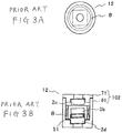
- Fig. 3 shows another example of a conventional optical isolator.
- Fig. 3A is a front elevational view while Fig. 3B is a side elevational view.
- an optical isolator 12 comprises a cylindrical metallic housing 102, two sheets of polarizers 2c and 2d, a Faraday rotator 3b and a ring-type magnet 8.
- the metallic housing 102 is composed in combination of a tubular housing member 61 and a cap-type housing member 71.
- the polarizer 2d, the Faraday rotator 3b and the ring-type magnet 8 are fixed in the tubular housing member 61, and polarizer 2c is fixed in the cap-type housing member 71.
- the ring-type magnet 8 is inserted at a peripheral portion of the Faraday rotator 3b.
- the ring-type magnet 8 is located to enclose the Faraday rotator 3b in order to provide magnetic field to the Faraday rctator 3b.
- a great deal of cost is required for processing the ring-type magnet 8.
- Fig. 4 is an explanatory view for showing an interim article to be processed in a method of manufacturing an optical component according to a preferred embodiment of the present invention.
- illustrated is the interim article to be processed (in other words, semi-manufactured article), in which long-shaped members (lengthy) 2e, 3a, 2f, 4a, each consisting of a material for each optical element and each cut into a strip having a width of 1.2 mm, are fixed on a substrate 1, respectively.
- the substrate 1 fixed are the long-shaped members (lengthy) 2e and 2f each consisting of a material for a polarizer, the long-shaped member (lengthy) 3a consisting of a material for a Faraday rotator, and the long-shaped member (lengthy) 4a consisting of a material for a compensator.
- the substrate 1 has a width of 3.1 mm.
- the substrate 1 consists of a magnetic material which can be welded.
- an Fe-Cr-Co magnetic material can be selected as the material of the substrate 1.
- an epoxy adhesive is coated on the substrate 1.
- the optical elements each cut into a strip having a width of 1.2 mm are positioned, respectively, by a positioning instrument (not shown) on the substrate 1. Thereafter, the optical elements are fixed thereon, respectively. With the condition, the substrate 1 and the optical elements fixed thereon are heated in an oven at a temperature of 120°C to harden the epoxy adhesive.
- the long-shaped members (lengthy) 2e and 2f each consisting of a material for a polarizer are used.
- An interim article to be processed can be similarly fabricated by alternatively using long-shaped members (lengthy) consisting of a material for a birefringent crystal.
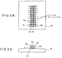
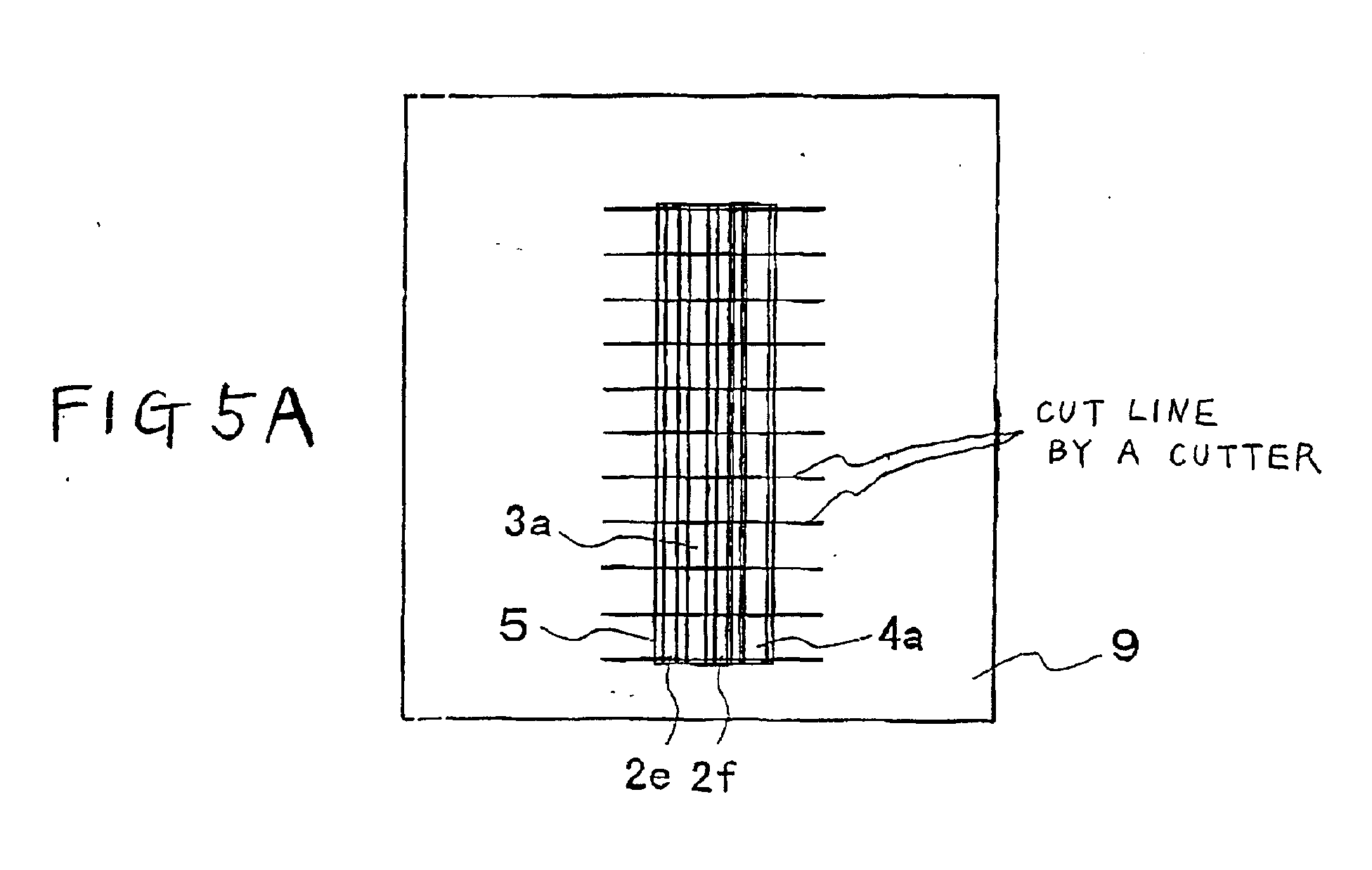
- Fig. 5 is an explanatory view for showing cutting process of the interim article to be processed in the method of manufacturing the optical component according to the preferred embodiment of the present invention.
- the interim article to be processed in which the epoxy adhesive is hardened by the oven is adhered on a glass substrate 9 by wax 10.
- the interim article to be processed is then cut by a cutter, as illustrated in Fig. 5A, into a plurality of pieces each of which has a width of 1.2 mm and each of which is used as an optical component.
- the optical component is an optical isolator which is an example of a non-reciprocal element.
- Fig. 6A is a front view for schematically showing the optical isolator while Fig. 6B is a side view for schematically showing the optical isolator.
- Fig. 6A three pieces of substrates 1d, le and if each of which is cut to have a size of 1.2mm x 3.1 mm are adhered and hardened on the optical isolator which is cut as illustrated in Figs. 5A and 5B.
- the optical isolator having the adhesive hardened therein is then inserted into a tubular housing member 6.
- the substrates lc, ld, le and lf are fixed at an end portion of the tubular housing member 6 by an adhesive, as shown in Fig. 6B.
- a cap-type housing member 7 is adhered and hardened on one lateral side of the above-mentioned tubular housing member 6. Accordingly, the optical isolator illustrated in Figs. 6A and 6B is obtained.
- optical insertion loss is 0.3 dB and the reverse direction loss is 25 dB.
- excellent optical characteristics are obtained in the optical isolator according to the above embodiment.
- a metallic housing 101 consisting of the tubular housing member 6 and a cap-type housing member 7 is used.
- an optical isolator according to another embodiment can be considered, in which no metallic housing is used.
- the substrates 1c, 1d, 1e and 1f can be fixed directly on an LD (Laser Diode) module, and the like, by welding, because the substrates 1c, 1d, 1e and 1f consist of magnets which can be welded.
- LD Laser Diode
- long-shaped members each of which is consisting of a material for each optical element and each of which is cut into a strip having a predetermined width are fixed on a substrate, respectively. Consequently, it becomes easy to make an optical component be positioned by an instrument. Therefore, it is possible to reduce not only slant or inclination of an optical element but also unnecessary deposition of an adhesive to the optical element. Accordingly, an optical component can be manufactured to have stable and reliable characteristics.
- optical elements each of which is cut into a strip having a predetermined width are fixed on a plate-like substrate, respectively. It thereby becomes possible to cut the optical component and the plate-like substrate simultaneously. Accordingly, it is possible to reduce man-hour for manufacturing the optical component to a large extent.
- the optical component it is not necessary to use a ring-shaped magnet by enclosing the optical component with four pieces of plate-like magnets.
- a processing cost of the plate-like magnet is smaller than that of the ring-shaped magnet. It is therefore possible to provide an 1 optical component which can be manufactured at a lower cost.
- the optical component is fixed by magnets which can be welded. It therefore becomes possible to make; the optical component be welded to an LD (Laser Diode) module, and the like, without the metallic housing. Accordingly, reduction of costs and down sizing of the optical component can be achieved.
- LD Laser Diode
- an optical component such as a non-reciprocal element, and a manufacturing method thereof, which has excellent optical characteristics; and excellent mass-productibility, and in which each optical element thereof is fixed securely.
Landscapes
- Physics & Mathematics (AREA)
- Nonlinear Science (AREA)
- General Physics & Mathematics (AREA)
- Optics & Photonics (AREA)
- Engineering & Computer Science (AREA)
- Power Engineering (AREA)
Abstract
Description
- The present invention relates to an optical component, such as a non-reciprocal element, which is favorable to be used mainly as an optical passive component for optical communication, and a method of manufacturing the optical component.
- Conventionally, an optical isolator has been used as an optical component for optical communication.
- As will later be described more in detail, a conventional optical isolator generally comprises first and second polarizers, a Faraday rotator, a compensator, first and second substrates. In a method of manufacturing the conventional optical isolator, the first polarizer, the Faraday rotator and the compensator are cut into a predetermined size and then fixed by an adhesive on the first substrate which is cut in a uniform size. Then, the second polarizer is adhered on the first substrate by adhesive. Thereafter, the second substrate is adhered on the first polarizer, the Faraday rotator, the compensator, and the second polarizer from the side thereof opposite to that of the first substrate.
- Another conventional optical isolator comprises a cylindrical metallic housing, primary and secondary polarizers, a Faraday rotator, and a ring-type magnet. Further, the metallic housing is composed in combination of a tubular housing member and a cap-type housing member. The primary polarizer, the Faraday rotator and the ring-type magnet is fixed in the tubular housing member while the secondary polarizer is fixed in the cap-type housing member. The ring-type magnet is inserted at a peripheral portion of the Faraday rotator.
- However, the method of manufacturing the conventional optical isolator has a problem of requiring a lot of working time for assembling optical elements. Further, in the event of mounting the optical elements on the first substrate by a pair of tweezers, the optical elements are attracted to each other by surface tension of the adhesive, the solder or the glass solder. Accordingly, characteristics of the conventional optical isolator may adversely affected because of deposition of adhesive, solder or glass solder on an optical surface or slant and inclination of be optical elements.
- Further, in the another conventional optical isolator, the ring-type magnet is located to enclose the Faraday rotatcr in order to provide magnetic field to the Faraday rotaton However, much cost is required for processing the ring-type magnet.
- Furthermore, for assembling the conventional optical isolators into an LD module, and the like, by welding, whole of the optical elements are inserted in a metallic case. However, it is difficult and requires much cost to fabricate the metallic case which is smaller in size. Accordingly, it is difficult to fabricate the conventional optical isolators in a small size at a low cost.
- It is therefore an object of the present invention to provide an optical component, such as a non-reciprocal element, which has excellent optical characteristics and excellent mass-poductibility, and in which each optical element therecf is fixed securely.
- It is another object of the present invention to provide a method of manufacturing the optical component which has excellent optical characteristics and excellent mass-productibility, and in which each optical element thereof is fixed securely.
- Other objects of the present invention will become clear as the description proceeds.
- In ar. optical component of the present invention, when a polarizer or a Faraday rotator is fixed on a substrate, it is not required to cut each of the above-mentioned optical elements into pieces. On the contrary, the optical component of the present invention is formed as follows. Namely, at first, the substrate is cut into a strip having a predetermined width while each of the optical elements is cut into a strip having a predetermined width. Next, each of the strip-shaped optical elements is fixed on the strip-shaped substrate. Then, the substrate and the optical elements fixed thereon are cut simultaneously, to have a predetermined size. Besides, a birefringent crystal can be alternatively used as the polarizer.
- The method of manufacturing the optical component of the present invention are carried out, as described below. At first, primary and secondary substrates are cut into a strip having a predetermined width while each of a polarizer or a birefringent crystal, and a Faraday rotator is cut into a strip having a predetermined width. Next, each of the strip-shaped polarizer or the strip-shaped birefringent crystal, and the strip-shaped Faraday rotator is fixed on the strip-shaped primary substi ate. Then, secondary substrate cut into a strip having a predetermined width is fixed on the strip-shaped polarizer or the strip-shaped birefringent crystal, and the strip-shaped Faraday rotator from another sides thereof opposite to the sides on which the primary substrate is fixed. Thereafter, the optical component is produced by cutting the optical elements and the primary and secondary substrates in a predetermined size simultaneously.
- Further, according to an optical component of the present invention, an optical component consisting of a non-reciprocal element, such as an optical isolator, an optical circulator, and the like is provided. In the optical component, a Faraday rotator can be supplied with magnetic field without using a ring-shaped magnet by enclosing a polarizer and the Faraday rotator with four pieces of plate-like magnets. A processing cost of a plate-like magnet is smaller than that of a ring type magnet. It is therefore possible to provide an optical component which can be manufactured at a lower cost.
- Furthermore, according to an optical component of the present invention, an optical component consisting of a non-reciprocal element, such as an optical isolator, an optical circulator, and the like is provided. In the optical component, it is not necessary to contain a polarizer and i Faraday rotator in a metallic housing by fixing the polarizer and the Faraday rotator on a substrate by the use of magnets which can be welded. Since the metallic housing is not required for the optical component, reduction of costs and down sizing of the optical component can be achieved. Besides, a birefringent crystal can be alternatively used as the polarizer.
- Moreover, according to a method of manufacturing an optical component of the present invention, a semi-manufactured article of the optical component is cut into a strip of a predetermined width and then fixed on a substrate. Consequently, it becomes easy to make an optical isolator, an optical circulator, and the like be positior.ed by an instrument. Therefore, it is possible to reduce not only slant or inclination of the optical component but also unnecessary deposition of an adhesive to the optical component. Accordingly, an optical component consisting of a non-reciprocal element, such as an optical isolator, an optical circulator, and the like, can be manufactured to have stable and reliable characteristics.
- In addition, according to a method of manufacturing an optical component of the present invention, the strip-shaped semi-manufactured article of the optical component may be fixed on a glass substrate. Thereafter, the strip-shaped semi-manufactured article of the optical component and the glass substrate may be cut simultaneously. Accordingly, it is possible to reduce man-hour for manufacturing the optical component to a large extent.
- Namely, according to an aspect of the present invention, there is provided an optical component comprising: polarizing means, a Faraday rotator and a substrate, the polarizing means and the Faraday rotator being fixed oil the substrate by at least two surfaces except for each optical surface thereof, respectively, the substrate consisting of magnet which can be welded.
- The polarizing means may be composed of a polarizer or a b:.refringent crystal.
- The cptical component may be for use in a non-reciprocal element, such as an optical isolator and an optical circulator.
- According to another aspect of the present invention, there is provided a method of manufacturing an optical component, the method comprising the steps of: preparing first lengthy consisting of a material for polarizing means; preparing second lengthy consisting of a material for a Faraday rotator; fixing the first lengthy and the second lengthy on a substrate; cutting the first lengthy, the second lengthy and the substrate through the whole thereof into a plurality of pieces each having a predetermined size; and each of the a plurality of pieces being used as the optical component. The polarizing means may be composed of two polarizers or two birefringent crystals.
- The substrate may consist of magnet which can be welded.
- According to still another aspect of the present invention, there is also provided a method of manufacturing an optical component, the method comprising the steps of: preparing first lengthy consisting of a material for polarizing means; preparing second lengthy consisting of a material for a Faraday rotator; fixing the first lengthy and the second lengthy by two substrate with the first lengthy and the second lengthy being interposed therebetween; cutting the first lengthy, the second lengthy and the two substrate through the whole thereof into a plurality of pieces each having a predetermined size; and each of the a plurality of pieces being used as the optical component.
-
- Fig. 1A is a front view for explaining an example of a conventional optical isolator;
- Fig. 1B is a side view for explaining the example of the conventional optical isolator illustrated in Fig. 1A;
- Fig. 2 is a view for schematically showing a conventional method of manufacturing an optical isolator;
- Fig. 3A is a front view for explaining another example of a conventional optical isolator;
- Fig. 3B is a side view for explaining the another example of the conventional optical isolator illustrated in Fig. 3A;
- Fig. 4 is an explanatory view for showing an article to be processed in a method of manufacturing an optical component according to a preferred embodiment of the present invention;
- Fig. 5A is a plan view for explaining cutting process of the interim article to be processed in the method of manufacturing the optical component according to the preferred embodiment of the present invention;
- Fig. 5B is a side view for explaining the cutting process of the interim article to be processed illustrated in Fig. 5A;
- Fig. 6A is a front view for schematically showing an optical isolator according to an embodiment of the present invention; and
- Fig. 6B is a side view for schematically showing the optical isolator illustrated in Fig. 6A.
-
- Referning to Figs. 1 through 3, description is, at first made about conventional optical components and a method of manufacturing one of the conventional optical components in order to facilitate an understanding of the present invention.
- Fig. 1 shows a conventional optical isolator. Fig. 1A is a front view of the conventional optical isolator while Fig. 1B is a side view thereof. In Figs. 1A and 1B, an
optical isolator 11 comprises two sheets ofpolarizers Faraday rotator 3b, acompensator 4b, and two sheets of substrate la and lb. In the illustrated example, materials of the substrate la and 1b are general ferritic magnetic materials. - Fig. 2 is an explanatory view for explaining a method of manufacturing the conventional
optical isolator 11 illustrated in Fig. 1. In Fig. 2, a semi-manufactured article of theoptical isolator 11 is composed ofpolarizer 2b,Faraday rotator 3b, a substrate la and thecompensator 4a Thepolarizer 2b, theFaraday rotator 3b and thecompensator 4b are cut into a predetermined size and then fixed by an adhesive on the substrate la which is cut in a uniform size. In the process of manufacturing theoptical isolator 11, the polarizer 16 is adhered on the substrate la by the adhesive 52 and the substrate lb is securely adhered on the opposite side of the substrate la in the above-mentioned semi-manufactured article. Besides, an organic adhesive, a solder or a glass solder is usable as the adhesive 52. - The conventional optical isolator and the method of manufacturing the conventional optical isolator have several problems, as mentioned below. The method of manufacturing the conventional optical isolator shown in Fig. 1 has a problem of requiring a lot of working time for the assembling. Further, as shown in Fig. 2, in the event of mounting optical elements on a substrate by a pair of tweezers, the optical elements are attracted to each other by surface tension of the adhesive, the solder or the glass solder. Accordingly, characteristics as an optical isolator may adversely affected because of deposition of adhesive, solder or glass solder on an optical surface or slant and inclination of an optical element.
- Fig. 3 shows another example of a conventional optical isolator. Fig. 3A is a front elevational view while Fig. 3B is a side elevational view. In Figs. 3A and 3B, an
optical isolator 12 comprises a cylindricalmetallic housing 102, two sheets ofpolarizers Faraday rotator 3b and a ring-type magnet 8. Further, themetallic housing 102 is composed in combination of a tubular housing member 61 and a cap-type housing member 71. Thepolarizer 2d, theFaraday rotator 3b and the ring-type magnet 8 are fixed in the tubular housing member 61, and polarizer 2c is fixed in the cap-type housing member 71. The ring-type magnet 8 is inserted at a peripheral portion of theFaraday rotator 3b. Thus, the ring-type magnet 8 is located to enclose theFaraday rotator 3b in order to provide magnetic field to theFaraday rctator 3b. However, a great deal of cost is required for processing the ring-type magnet 8. - Furthermore, for assembling the conventional optical isolators of Fig. 1 and Fig. 3 into an LD module, and the like, by welding, whole portions of the optical elements are inserted in a metallic case. However, producing such a metallic case in smaller size is limited and requires high cost. Accordingly, it is difficult to fabricate the conventional optical isolator in a small size at a low cost.
- Referning to Figs. 4 through 6, description will proceed to an optical component and a method of manufacturing the optical component according to embodiments of the present invention.
- Fig. 4 is an explanatory view for showing an interim article to be processed in a method of manufacturing an optical component according to a preferred embodiment of the present invention. In Fig. 4, illustrated is the interim article to be processed (in other words, semi-manufactured article), in which long-shaped members (lengthy) 2e, 3a, 2f, 4a, each consisting of a material for each optical element and each cut into a strip having a width of 1.2 mm, are fixed on a
substrate 1, respectively. Namely, on thesubstrate 1, fixed are the long-shaped members (lengthy) 2e and 2f each consisting of a material for a polarizer, the long-shaped member (lengthy) 3a consisting of a material for a Faraday rotator, and the long-shaped member (lengthy) 4a consisting of a material for a compensator. Herein, thesubstrate 1 has a width of 3.1 mm. In addition, thesubstrate 1 consists of a magnetic material which can be welded. For example, an Fe-Cr-Co magnetic material can be selected as the material of thesubstrate 1. - In order to fabricate the interim article illustrated in F.g. 4, at first, an epoxy adhesive is coated on the
substrate 1. The optical elements each cut into a strip having a width of 1.2 mm are positioned, respectively, by a positioning instrument (not shown) on thesubstrate 1. Thereafter, the optical elements are fixed thereon, respectively. With the condition, thesubstrate 1 and the optical elements fixed thereon are heated in an oven at a temperature of 120°C to harden the epoxy adhesive. - In the example illustrated in Fig. 4, the long-shaped members (lengthy) 2e and 2f each consisting of a material for a polarizer are used. An interim article to be processed can be similarly fabricated by alternatively using long-shaped members (lengthy) consisting of a material for a birefringent crystal.
- Fig. 5 is an explanatory view for showing cutting process of the interim article to be processed in the method of manufacturing the optical component according to the preferred embodiment of the present invention. As illustrated in Figs. 5A and 5B, the interim article to be processed in which the epoxy adhesive is hardened by the oven is adhered on a glass substrate 9 by
wax 10. The interim article to be processed is then cut by a cutter, as illustrated in Fig. 5A, into a plurality of pieces each of which has a width of 1.2 mm and each of which is used as an optical component. Herein, the optical component is an optical isolator which is an example of a non-reciprocal element. - Fig. 6A is a front view for schematically showing the optical isolator while Fig. 6B is a side view for schematically showing the optical isolator. As illustrated in Fig. 6A, three pieces of
substrates 1d, le and if each of which is cut to have a size of 1.2mm x 3.1 mm are adhered and hardened on the optical isolator which is cut as illustrated in Figs. 5A and 5B. The optical isolator having the adhesive hardened therein is then inserted into a tubular housing member 6. The substrates lc, ld, le and lf are fixed at an end portion of the tubular housing member 6 by an adhesive, as shown in Fig. 6B. Thereafter, a cap-type housing member 7 is adhered and hardened on one lateral side of the above-mentioned tubular housing member 6. Accordingly, the optical isolator illustrated in Figs. 6A and 6B is obtained. - In order to confirm optical characteristics of the optical isolator according to the above embodiment, an optical insertion loss and a reverse direction loss were investigated. As a result, it was confirmed that the optical insertion loss is 0.3 dB and the reverse direction loss is 25 dB. Thus, excellent optical characteristics are obtained in the optical isolator according to the above embodiment.
- In the optical isolator according to the above embodiment, a
metallic housing 101 consisting of the tubular housing member 6 and a cap-type housing member 7 is used. However, an optical isolator according to another embodiment can be considered, in which no metallic housing is used. In this case, thesubstrates substrates - As described above, according to the present invention, long-shaped members (lengthy) each of which is consisting of a material for each optical element and each of which is cut into a strip having a predetermined width are fixed on a substrate, respectively. Consequently, it becomes easy to make an optical component be positioned by an instrument. Therefore, it is possible to reduce not only slant or inclination of an optical element but also unnecessary deposition of an adhesive to the optical element. Accordingly, an optical component can be manufactured to have stable and reliable characteristics.
- Further, according to the present invention, optical elements each of which is cut into a strip having a predetermined width are fixed on a plate-like substrate, respectively. It thereby becomes possible to cut the optical component and the plate-like substrate simultaneously. Accordingly, it is possible to reduce man-hour for manufacturing the optical component to a large extent.
- Furthermore, in the optical component, it is not necessary to use a ring-shaped magnet by enclosing the optical component with four pieces of plate-like magnets. A processing cost of the plate-like magnet is smaller than that of the ring-shaped magnet. It is therefore possible to provide an 1 optical component which can be manufactured at a lower cost.
- Moreover, the optical component is fixed by magnets which can be welded. It therefore becomes possible to make; the optical component be welded to an LD (Laser Diode) module, and the like, without the metallic housing. Accordingly, reduction of costs and down sizing of the optical component can be achieved.
- As mentioned above, according to the present invention, it is possible to provide an optical component, such as a non-reciprocal element, and a manufacturing method thereof, which has excellent optical characteristics; and excellent mass-productibility, and in which each optical element thereof is fixed securely.
Claims (10)
- An optical component comprising: polarizing means, a Faraday rotator and a substrate, said polarizing means and said Faraday rotator being fixed on said substrate by at least two surfaces except for each optical surface thereof, respectively, said substrate consisting of magnet which can be welded.
- An optical component as claimed in claim 1, wherein said polarizing means is composed of a polarizer or of a birefringent crystal.
- An optical component as claimed in claim 1 or 2, wherein said optical component is for use in a non-reciprocal element.
- An optical component as claimed in claim 3, wherein said non-reciprocal element is an optical isolator or an optical circulator.
- A method of manufacturing an optical component, said method comprising the steps of:preparing first lenghty consisting of a material for polarizing means;preparing second lengthy consisting of a material for a Faraday rotator;fixing said first lengthy and said second lenghty on a substrate;cutting said first lengthy, said second lengthy and said substrate through the whole thereof into a plurality of pieces each having a predetermined size; andeach of said a plurality of pieces being used as said optical component.
- A method of manufacturing an optical component, said method comprising the steps of:preparing first lengthy consisting of a material for polarizing means;preparing second lenghty consisting of a material for a Faraday rotator;fixing said first lengthy and said second lengthy by two substrate with said first lengthy and said second lengthy being interposed therebetween;cutting said first lengthy, said second lengthy and said two substrate through the whole thereof into a plurality of pieces each having a predetermined size; andeach of said a plurality of pieces being used as said optical component.
- A method as claimed in claim 5 or 6, wherein said polarizing means are composed of two polarizers or of two birefringent crystals.
- A method as claimed in one of claims 5 to 7, wherein said substrate consists of magnet which can be welded.
- A method as claimed in one of claims 5 to 8, wherein said optical component is for use in a non-reciprocal element.
- A method as claimed in claim 9, wherein said non-reciprocal element is an optical isolator or an optical circulator.
Applications Claiming Priority (2)
| Application Number | Priority Date | Filing Date | Title |
|---|---|---|---|
| JP30719499 | 1999-10-28 | ||
| JP30719499A JP4351339B2 (en) | 1999-10-28 | 1999-10-28 | Manufacturing method of optical components |
Publications (2)
| Publication Number | Publication Date |
|---|---|
| EP1096299A1 true EP1096299A1 (en) | 2001-05-02 |
| EP1096299B1 EP1096299B1 (en) | 2004-09-08 |
Family
ID=17966183
Family Applications (1)
| Application Number | Title | Priority Date | Filing Date |
|---|---|---|---|
| EP00123554A Expired - Lifetime EP1096299B1 (en) | 1999-10-28 | 2000-10-27 | Optical component and method of manufacturing the same |
Country Status (9)
| Country | Link |
|---|---|
| US (1) | US6529324B1 (en) |
| EP (1) | EP1096299B1 (en) |
| JP (1) | JP4351339B2 (en) |
| KR (1) | KR100429492B1 (en) |
| CN (1) | CN1157627C (en) |
| AU (1) | AU780128B2 (en) |
| CA (1) | CA2324530A1 (en) |
| DE (1) | DE60013530T2 (en) |
| TW (1) | TW460711B (en) |
Families Citing this family (4)
| Publication number | Priority date | Publication date | Assignee | Title |
|---|---|---|---|---|
| JP3459047B2 (en) | 2002-09-24 | 2003-10-20 | Tdk株式会社 | Manufacturing method of embedded optical isolator using polarizing glass |
| KR20030078047A (en) * | 2003-08-26 | 2003-10-04 | (주)포인테크 | Alignment Method of Multiple Optical Fibers to Parallely Arranged Multiple Optical Waveguide Chips |
| CN112799186A (en) * | 2021-04-14 | 2021-05-14 | 武汉恩达通科技有限公司 | Four-port circulator with multiple isolators and coherent BIDI optical module |
| JP7811903B2 (en) * | 2022-12-28 | 2026-02-06 | 信越化学工業株式会社 | Optical isolator and method for manufacturing the same |
Citations (5)
| Publication number | Priority date | Publication date | Assignee | Title |
|---|---|---|---|---|
| JPH08338965A (en) * | 1995-06-12 | 1996-12-24 | Tokin Corp | Optical isolator |
| EP0785456A1 (en) * | 1996-01-17 | 1997-07-23 | Hewlett-Packard Company | Optical isolator |
| JPH10227996A (en) * | 1997-02-14 | 1998-08-25 | Sumitomo Metal Mining Co Ltd | Optical isolator |
| JPH10333096A (en) * | 1997-05-30 | 1998-12-18 | Kyocera Corp | Optical isolator element and method of manufacturing the same |
| US5867314A (en) * | 1993-12-09 | 1999-02-02 | Fuji Electrochemical Co., Ltd. | Structure of optical passive device and assembling method therefor |
Family Cites Families (7)
| Publication number | Priority date | Publication date | Assignee | Title |
|---|---|---|---|---|
| JP2689073B2 (en) * | 1993-12-09 | 1997-12-10 | 富士電気化学株式会社 | Optical isolator |
| KR960002989A (en) * | 1994-06-29 | 1996-01-26 | 김정덕 | Optical isolator |
| JPH1068907A (en) * | 1996-08-27 | 1998-03-10 | Fuji Elelctrochem Co Ltd | Optical isolator |
| JP3570869B2 (en) * | 1997-09-26 | 2004-09-29 | 京セラ株式会社 | Optical isolator element and method of manufacturing the same |
| JP3645700B2 (en) * | 1997-12-22 | 2005-05-11 | 京セラ株式会社 | Optical isolator element and manufacturing method thereof |
| JPH11183841A (en) * | 1997-12-22 | 1999-07-09 | Kyocera Corp | Optical isolator element, method of manufacturing the same, and optical module |
| JP2001242419A (en) * | 2000-02-28 | 2001-09-07 | Oyokoden Lab Co Ltd | Method for manufacturing optical isolator and optical isolator |
-
1999
- 1999-10-28 JP JP30719499A patent/JP4351339B2/en not_active Expired - Fee Related
-
2000
- 2000-10-26 US US09/696,682 patent/US6529324B1/en not_active Expired - Fee Related
- 2000-10-27 EP EP00123554A patent/EP1096299B1/en not_active Expired - Lifetime
- 2000-10-27 DE DE60013530T patent/DE60013530T2/en not_active Expired - Fee Related
- 2000-10-27 AU AU69588/00A patent/AU780128B2/en not_active Ceased
- 2000-10-27 CA CA002324530A patent/CA2324530A1/en not_active Abandoned
- 2000-10-27 CN CNB001302132A patent/CN1157627C/en not_active Expired - Fee Related
- 2000-10-27 TW TW089122724A patent/TW460711B/en active
- 2000-10-28 KR KR10-2000-0063743A patent/KR100429492B1/en not_active Expired - Fee Related
Patent Citations (5)
| Publication number | Priority date | Publication date | Assignee | Title |
|---|---|---|---|---|
| US5867314A (en) * | 1993-12-09 | 1999-02-02 | Fuji Electrochemical Co., Ltd. | Structure of optical passive device and assembling method therefor |
| JPH08338965A (en) * | 1995-06-12 | 1996-12-24 | Tokin Corp | Optical isolator |
| EP0785456A1 (en) * | 1996-01-17 | 1997-07-23 | Hewlett-Packard Company | Optical isolator |
| JPH10227996A (en) * | 1997-02-14 | 1998-08-25 | Sumitomo Metal Mining Co Ltd | Optical isolator |
| JPH10333096A (en) * | 1997-05-30 | 1998-12-18 | Kyocera Corp | Optical isolator element and method of manufacturing the same |
Non-Patent Citations (4)
| Title |
|---|
| DATABASE WPI Week 199910, Derwent World Patents Index; AN 1999-110071, XP002157650 * |
| PATENT ABSTRACTS OF JAPAN vol. 1997, no. 04 30 April 1997 (1997-04-30) * |
| PATENT ABSTRACTS OF JAPAN vol. 1998, no. 13 30 November 1998 (1998-11-30) * |
| PATENT ABSTRACTS OF JAPAN vol. 1999, no. 03 31 March 1999 (1999-03-31) * |
Also Published As
| Publication number | Publication date |
|---|---|
| CN1295263A (en) | 2001-05-16 |
| KR20010060216A (en) | 2001-07-06 |
| DE60013530T2 (en) | 2005-09-15 |
| TW460711B (en) | 2001-10-21 |
| US6529324B1 (en) | 2003-03-04 |
| KR100429492B1 (en) | 2004-05-03 |
| CA2324530A1 (en) | 2001-04-28 |
| JP4351339B2 (en) | 2009-10-28 |
| EP1096299B1 (en) | 2004-09-08 |
| DE60013530D1 (en) | 2004-10-14 |
| AU6958800A (en) | 2001-05-03 |
| AU780128B2 (en) | 2005-03-03 |
| CN1157627C (en) | 2004-07-14 |
| JP2001125045A (en) | 2001-05-11 |
Similar Documents
| Publication | Publication Date | Title |
|---|---|---|
| EP0785456B1 (en) | Fabrication of optical isolators | |
| KR20010077884A (en) | Optical isolator comprising a faraday rotator | |
| EP1096299A1 (en) | Optical component and method of manufacturing the same | |
| US6028702A (en) | Optical isolator | |
| JP4548988B2 (en) | Receptacle with optical isolator and its assembly method | |
| JP2001264694A (en) | Polarization-independent optical isolator | |
| JPH11167085A (en) | Optical isolator and optical fiber terminal with optical isolator | |
| JP4540155B2 (en) | Optical isolator | |
| JP3290474B2 (en) | Optical isolator for semiconductor laser array | |
| US20030002128A1 (en) | Optical isolator | |
| JP2002196282A (en) | Optical isolator | |
| JP2003315736A (en) | Optical isolator | |
| JP2005215328A (en) | Optical isolator | |
| JP3990088B2 (en) | Optical isolator | |
| JP2002082309A (en) | Optical isolator | |
| JP3881555B2 (en) | Ferrule for optical fiber and stub and receptacle with optical isolator using the same | |
| JPH0933860A (en) | Optical connector | |
| JP2006126607A (en) | Optical isolator | |
| JP2003090984A (en) | Embedded optical isolator | |
| JP2001013459A (en) | Optical isolator | |
| JP4456223B2 (en) | Optical isolator | |
| JPH11183841A (en) | Optical isolator element, method of manufacturing the same, and optical module | |
| JPH09138372A (en) | Optical isolator | |
| JPH07120703A (en) | Method for manufacturing optical isolator element having optical fiber support | |
| JP2000206461A (en) | Optical circulator |
Legal Events
| Date | Code | Title | Description |
|---|---|---|---|
| PUAI | Public reference made under article 153(3) epc to a published international application that has entered the european phase |
Free format text: ORIGINAL CODE: 0009012 |
|
| AK | Designated contracting states |
Kind code of ref document: A1 Designated state(s): DE FR GB IT |
|
| AX | Request for extension of the european patent |
Free format text: AL;LT;LV;MK;RO;SI |
|
| 17P | Request for examination filed |
Effective date: 20011023 |
|
| AKX | Designation fees paid |
Free format text: DE FR GB IT |
|
| 17Q | First examination report despatched |
Effective date: 20020424 |
|
| RAP1 | Party data changed (applicant data changed or rights of an application transferred) |
Owner name: NEC TOKIN CORPORATION |
|
| GRAP | Despatch of communication of intention to grant a patent |
Free format text: ORIGINAL CODE: EPIDOSNIGR1 |
|
| GRAS | Grant fee paid |
Free format text: ORIGINAL CODE: EPIDOSNIGR3 |
|
| GRAA | (expected) grant |
Free format text: ORIGINAL CODE: 0009210 |
|
| RIN1 | Information on inventor provided before grant (corrected) |
Inventor name: HOSOKAWA, TADATOSHI,C/O TOKIN CORPORATION Inventor name: TSUCHIYA, HARUHIKO,C/O TOKIN CORPORATION Inventor name: MIURA, HIDESHI,C/O TOKIN CORPORATION Inventor name: TOKAIRIN, TOSHIO,C/O TOKIN CORPORATION |
|
| AK | Designated contracting states |
Kind code of ref document: B1 Designated state(s): DE FR GB IT |
|
| REG | Reference to a national code |
Ref country code: GB Ref legal event code: FG4D |
|
| REF | Corresponds to: |
Ref document number: 60013530 Country of ref document: DE Date of ref document: 20041014 Kind code of ref document: P |
|
| ET | Fr: translation filed | ||
| PLBE | No opposition filed within time limit |
Free format text: ORIGINAL CODE: 0009261 |
|
| STAA | Information on the status of an ep patent application or granted ep patent |
Free format text: STATUS: NO OPPOSITION FILED WITHIN TIME LIMIT |
|
| 26N | No opposition filed |
Effective date: 20050609 |
|
| PGFP | Annual fee paid to national office [announced via postgrant information from national office to epo] |
Ref country code: FR Payment date: 20051010 Year of fee payment: 6 |
|
| PGFP | Annual fee paid to national office [announced via postgrant information from national office to epo] |
Ref country code: DE Payment date: 20051020 Year of fee payment: 6 |
|
| PGFP | Annual fee paid to national office [announced via postgrant information from national office to epo] |
Ref country code: GB Payment date: 20051026 Year of fee payment: 6 |
|
| PGFP | Annual fee paid to national office [announced via postgrant information from national office to epo] |
Ref country code: IT Payment date: 20061031 Year of fee payment: 7 |
|
| PG25 | Lapsed in a contracting state [announced via postgrant information from national office to epo] |
Ref country code: DE Free format text: LAPSE BECAUSE OF NON-PAYMENT OF DUE FEES Effective date: 20070501 |
|
| GBPC | Gb: european patent ceased through non-payment of renewal fee |
Effective date: 20061027 |
|
| REG | Reference to a national code |
Ref country code: FR Ref legal event code: ST Effective date: 20070629 |
|
| PG25 | Lapsed in a contracting state [announced via postgrant information from national office to epo] |
Ref country code: GB Free format text: LAPSE BECAUSE OF NON-PAYMENT OF DUE FEES Effective date: 20061027 |
|
| PG25 | Lapsed in a contracting state [announced via postgrant information from national office to epo] |
Ref country code: FR Free format text: LAPSE BECAUSE OF NON-PAYMENT OF DUE FEES Effective date: 20061031 |
|
| PG25 | Lapsed in a contracting state [announced via postgrant information from national office to epo] |
Ref country code: IT Free format text: LAPSE BECAUSE OF NON-PAYMENT OF DUE FEES Effective date: 20071027 |