EP1094625A2 - Dispersion slope equalizer - Google Patents
Dispersion slope equalizer Download PDFInfo
- Publication number
- EP1094625A2 EP1094625A2 EP00309165A EP00309165A EP1094625A2 EP 1094625 A2 EP1094625 A2 EP 1094625A2 EP 00309165 A EP00309165 A EP 00309165A EP 00309165 A EP00309165 A EP 00309165A EP 1094625 A2 EP1094625 A2 EP 1094625A2
- Authority
- EP
- European Patent Office
- Prior art keywords
- dispersion slope
- wavelength
- waveguide
- waveguides
- dispersion
- Prior art date
- Legal status (The legal status is an assumption and is not a legal conclusion. Google has not performed a legal analysis and makes no representation as to the accuracy of the status listed.)
- Granted
Links
Images


Classifications
-
- G—PHYSICS
- G02—OPTICS
- G02B—OPTICAL ELEMENTS, SYSTEMS OR APPARATUS
- G02B6/00—Light guides; Structural details of arrangements comprising light guides and other optical elements, e.g. couplings
- G02B6/24—Coupling light guides
- G02B6/26—Optical coupling means
- G02B6/28—Optical coupling means having data bus means, i.e. plural waveguides interconnected and providing an inherently bidirectional system by mixing and splitting signals
- G02B6/293—Optical coupling means having data bus means, i.e. plural waveguides interconnected and providing an inherently bidirectional system by mixing and splitting signals with wavelength selective means
- G02B6/29379—Optical coupling means having data bus means, i.e. plural waveguides interconnected and providing an inherently bidirectional system by mixing and splitting signals with wavelength selective means characterised by the function or use of the complete device
- G02B6/29392—Controlling dispersion
- G02B6/29394—Compensating wavelength dispersion
-
- G—PHYSICS
- G02—OPTICS
- G02B—OPTICAL ELEMENTS, SYSTEMS OR APPARATUS
- G02B6/00—Light guides; Structural details of arrangements comprising light guides and other optical elements, e.g. couplings
- G02B6/10—Light guides; Structural details of arrangements comprising light guides and other optical elements, e.g. couplings of the optical waveguide type
- G02B6/12—Light guides; Structural details of arrangements comprising light guides and other optical elements, e.g. couplings of the optical waveguide type of the integrated circuit kind
- G02B6/12007—Light guides; Structural details of arrangements comprising light guides and other optical elements, e.g. couplings of the optical waveguide type of the integrated circuit kind forming wavelength selective elements, e.g. multiplexer, demultiplexer
- G02B6/12009—Light guides; Structural details of arrangements comprising light guides and other optical elements, e.g. couplings of the optical waveguide type of the integrated circuit kind forming wavelength selective elements, e.g. multiplexer, demultiplexer comprising arrayed waveguide grating [AWG] devices, i.e. with a phased array of waveguides
- G02B6/12019—Light guides; Structural details of arrangements comprising light guides and other optical elements, e.g. couplings of the optical waveguide type of the integrated circuit kind forming wavelength selective elements, e.g. multiplexer, demultiplexer comprising arrayed waveguide grating [AWG] devices, i.e. with a phased array of waveguides characterised by the optical interconnection to or from the AWG devices, e.g. integration or coupling with lasers or photodiodes
- G02B6/12021—Comprising cascaded AWG devices; AWG multipass configuration; Plural AWG devices integrated on a single chip
-
- G—PHYSICS
- G02—OPTICS
- G02B—OPTICAL ELEMENTS, SYSTEMS OR APPARATUS
- G02B6/00—Light guides; Structural details of arrangements comprising light guides and other optical elements, e.g. couplings
- G02B6/24—Coupling light guides
- G02B6/26—Optical coupling means
- G02B6/28—Optical coupling means having data bus means, i.e. plural waveguides interconnected and providing an inherently bidirectional system by mixing and splitting signals
- G02B6/293—Optical coupling means having data bus means, i.e. plural waveguides interconnected and providing an inherently bidirectional system by mixing and splitting signals with wavelength selective means
- G02B6/29346—Optical coupling means having data bus means, i.e. plural waveguides interconnected and providing an inherently bidirectional system by mixing and splitting signals with wavelength selective means operating by wave or beam interference
- G02B6/2935—Mach-Zehnder configuration, i.e. comprising separate splitting and combining means
- G02B6/29352—Mach-Zehnder configuration, i.e. comprising separate splitting and combining means in a light guide
- G02B6/29355—Cascade arrangement of interferometers
-
- G—PHYSICS
- G02—OPTICS
- G02B—OPTICAL ELEMENTS, SYSTEMS OR APPARATUS
- G02B6/00—Light guides; Structural details of arrangements comprising light guides and other optical elements, e.g. couplings
- G02B6/24—Coupling light guides
- G02B6/26—Optical coupling means
- G02B6/28—Optical coupling means having data bus means, i.e. plural waveguides interconnected and providing an inherently bidirectional system by mixing and splitting signals
- G02B6/293—Optical coupling means having data bus means, i.e. plural waveguides interconnected and providing an inherently bidirectional system by mixing and splitting signals with wavelength selective means
- G02B6/29379—Optical coupling means having data bus means, i.e. plural waveguides interconnected and providing an inherently bidirectional system by mixing and splitting signals with wavelength selective means characterised by the function or use of the complete device
- G02B6/29395—Optical coupling means having data bus means, i.e. plural waveguides interconnected and providing an inherently bidirectional system by mixing and splitting signals with wavelength selective means characterised by the function or use of the complete device configurable, e.g. tunable or reconfigurable
-
- H—ELECTRICITY
- H04—ELECTRIC COMMUNICATION TECHNIQUE
- H04B—TRANSMISSION
- H04B10/00—Transmission systems employing electromagnetic waves other than radio-waves, e.g. infrared, visible or ultraviolet light, or employing corpuscular radiation, e.g. quantum communication
- H04B10/25—Arrangements specific to fibre transmission
- H04B10/2507—Arrangements specific to fibre transmission for the reduction or elimination of distortion or dispersion
- H04B10/2513—Arrangements specific to fibre transmission for the reduction or elimination of distortion or dispersion due to chromatic dispersion
- H04B10/25133—Arrangements specific to fibre transmission for the reduction or elimination of distortion or dispersion due to chromatic dispersion including a lumped electrical or optical dispersion compensator
-
- G—PHYSICS
- G02—OPTICS
- G02B—OPTICAL ELEMENTS, SYSTEMS OR APPARATUS
- G02B6/00—Light guides; Structural details of arrangements comprising light guides and other optical elements, e.g. couplings
- G02B6/24—Coupling light guides
- G02B6/26—Optical coupling means
- G02B6/28—Optical coupling means having data bus means, i.e. plural waveguides interconnected and providing an inherently bidirectional system by mixing and splitting signals
- G02B6/293—Optical coupling means having data bus means, i.e. plural waveguides interconnected and providing an inherently bidirectional system by mixing and splitting signals with wavelength selective means
- G02B6/29346—Optical coupling means having data bus means, i.e. plural waveguides interconnected and providing an inherently bidirectional system by mixing and splitting signals with wavelength selective means operating by wave or beam interference
- G02B6/2935—Mach-Zehnder configuration, i.e. comprising separate splitting and combining means
- G02B6/29352—Mach-Zehnder configuration, i.e. comprising separate splitting and combining means in a light guide
- G02B6/29353—Mach-Zehnder configuration, i.e. comprising separate splitting and combining means in a light guide with a wavelength selective element in at least one light guide interferometer arm, e.g. grating, interference filter, resonator
-
- G—PHYSICS
- G02—OPTICS
- G02B—OPTICAL ELEMENTS, SYSTEMS OR APPARATUS
- G02B6/00—Light guides; Structural details of arrangements comprising light guides and other optical elements, e.g. couplings
- G02B6/24—Coupling light guides
- G02B6/26—Optical coupling means
- G02B6/28—Optical coupling means having data bus means, i.e. plural waveguides interconnected and providing an inherently bidirectional system by mixing and splitting signals
- G02B6/293—Optical coupling means having data bus means, i.e. plural waveguides interconnected and providing an inherently bidirectional system by mixing and splitting signals with wavelength selective means
- G02B6/29379—Optical coupling means having data bus means, i.e. plural waveguides interconnected and providing an inherently bidirectional system by mixing and splitting signals with wavelength selective means characterised by the function or use of the complete device
- G02B6/29398—Temperature insensitivity
-
- H—ELECTRICITY
- H04—ELECTRIC COMMUNICATION TECHNIQUE
- H04B—TRANSMISSION
- H04B2210/00—Indexing scheme relating to optical transmission systems
- H04B2210/25—Distortion or dispersion compensation
- H04B2210/258—Distortion or dispersion compensation treating each wavelength or wavelength band separately
Definitions
- the present invention is on a dispersion slope equalizer that simultaneously recovers waveforms of wavelength division multiplexed (WDM) signals distorted by dispersion characteristic (that is; group delay is different at each wavelength) in an optical fiber.
- WDM wavelength division multiplexed
- DSF dispersion shifted fiber
- NZ-DSF non-zero dispersion shifted fiber
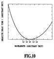
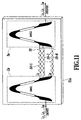
- second-order dispersion (derivative of group delay with respect to wavelength) is different at each wavelength channel as shown in Fig. 20 (relative delay time characteristics of DSF).
- This dispersion difference is caused by dispersion slope, namely, third-order dispersion (derivative of second-order dispersion with respect to wavelength), whose typical value is about 0.07 psec/nm 2 /km.
- the signal pulse at each wavelength channel is differently distorted, which limits (distance between repeaters). This is also the same as when NZ-DSF is used.
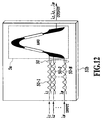
- Fig. 21 configuration in Fig. 21 has been known as a dispersion slope equalizer, which recovers the distorted waveforms of WDM signals by the dispersion in fibers.
- dispersion compensating fiber (DCF) 44 is set behind fiber transmission line 43.
- dispersion characteristic in the fiber transmission line can be compensated by the DCF, whose dispersion has the same absolute value with opposite sign to that of the fiber transmission line.
- an object of the present invention is to provide a compact dispersion slope equalizer by which it is possible to simultaneously recover distorted waveforms of WDM signals by dispersion slope of DSF or NZ-DSF at 1.55 ⁇ m band, and to compensate for the dispersion of various fiber transmission lines having various dispersion values and variation of dispersion value caused by the temperature change or the like.
- This configuration comprises group delay controllers comprising lattice-form optical circuits, transversal-form optical circuits, or the combination of these two circuits.
- a dispersion slope equalizer for compensating signal distortion caused by dispersion slope of a transmission line when transmitting lightwaves with plural wavelength signals in the transmission line characterized by comprising: N (N: natural number) waveguides, N output wavelength demultiplexer and/or N input wavelength multiplexer, and K (K: natural number, K ⁇ N) group delay controllers; the N waveguides being connected to outputs of the wavelength demultiplexer and/or inputs of the wavelength multiplexer; in the group delay controllers, one or both of input/output parts of lattice-form optical circuits being set on the N waveguides; wherein the lattice-form optical circuits are composed of two waveguides interleaved with at least two directional couplers, and the two waveguides are designed so that optical path lengths between the directional couplers are different.
- the wavelength demultiplexer and the wavelength multiplexer are arrayed-waveguide gratings.
- the group delay controllers are connected to N input wavelength multiplexer and the N waveguides are connected to only inputs of the wavelength multiplexer.
- the wavelength multiplexer is an arrayed-waveguide grating.
- the group delay controllers are connected to N output wavelength demultiplexer and the N waveguides are connected to only outputs of the wavelength demultiplexer.
- the wavelength demultiplexer is an arrayed-waveguide grating.
- the group delay controllers are composed of the combination of the lattice-form and transversal-form optical circuits.
- a dispersion slope equalizer for compensating signal distortion caused by dispersion slope of a transmission line when transmitting lightwaves with plural wavelength signals in the transmission line characterized by comprising: N (N: natural number) waveguides, N output wavelength demultiplexer and/or N input wavelength multiplexer, and N group delay controllers; the N waveguides being connected to outputs of the wavelength demultiplexer and/or inputs of the wavelength multiplexer; in the group delay controllers, one of inputs and an output of transversal-form optical circuits being set on the N waveguides; wherein the transversal-form optical circuit is provided with first waveguide for one of inputs and M (M: natural number, M ⁇ 2)directional couplers for coupling M waveguides with the first waveguide at M different positions, and the M waveguides, after being coupled with the first waveguide, are multiplexed by a multiplexer into second output waveguide.
- N natural number
- the wavelength demultiplexer and the wavelength multiplexer are arrayed-waveguide gratings.
- the group delay controllers are connected to N input wavelength multiplexer and the N waveguides are connected to only inputs of the wavelength multiplexer.
- the wavelength multiplexer is an arrayed-waveguide grating.
- the group delay controllers are connected to N outputs wavelength demultiplexer and the N waveguides are connected to only outputs of the wavelength demultiplexer.
- the wavelength demultiplexer is an arrayed-waveguide grating.
- the group delay controllers are composed of the combination of the transversal-form and lattice-form optical circuits.
- the dispersion slope equalizer according to the present invention comprises integrated-optic components, that is; a wavelength demultiplexer and/or a wavelength multiplexer and a lattice-form optical circuit and/or a transversal-form optical circuit.
- integrated-optic components that is; a wavelength demultiplexer and/or a wavelength multiplexer and a lattice-form optical circuit and/or a transversal-form optical circuit.
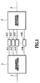
- Fig. 1 is a diagram showing the configuration of a first embodiment of the dispersion slope equalizer according to the present invention
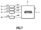
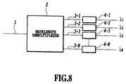
- the dispersion slope equalizer of the present embodiment comprises an input waveguide 1, a wavelength demultiplexer 2, waveguides 3-1 to 3-N, lattice-form optical circuits 4-1 to 4-N, a wavelength multiplexer 5, and an output waveguide 6.
- WDM signal lightwaves ⁇ 1 to ⁇ N distorted by the dispersion slope are introduced into the input waveguide 1 and are demultiplexed by the wavelength demultiplexer 2 into wavelength components. Then, these wavelength components are introduced into the lattice-form optical circuits 4-1 to 4-N for dispersion slope compensation, and are multiplexed by the wavelength multiplexer 5. Finally, the multiplexed lightwaves are outputted at the output waveguide 6, thus achieving the dispersion slope equalizer.
- the wavelength demultiplexer 2 and the wavelength multiplexer 5 can be composed of not only arrayed-waveguide gratings (described in detail later), but also cascaded configuration of Mach-Zehnder interferometers, bulk-type optical filters, or fiber-type (or waveguide-type) gratings in series.
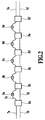
- Fig. 2 is a diagram showing a configuration example of the lattice-form optical circuits 4-1 to 4-N.
- This lattice-form optical circuit has a configuration in which five asymmetrical arm pairs are cascaded in series by setting six directional couplers, that is; asymmetrical Mach-Zehnder interferometers are cascaded in series.
- 7a to 7f are waveguides (waveguides 7a and 7b, and 7e and 7f are inputs and outputs, respectively)
- 8a to 8f are directional couplers
- 9a to 9e are control parts of waveguide refractive index.
- Fig. 1 Four lattice-form optical circuits 4-1 to 4-N in Fig. 1 are connected to one of waveguides 3-1 to 3-N by utilizing one of the waveguides 7a and 7b and one of the waveguides 7e and 7f.
- the directional couplers 8a to 8f can have a configuration in which the two waveguides 10a and 10b are made approached each other, or a multi-mode interference (MMI) coupler configuration.
- MMI multi-mode interference
- the coupling coefficient is fixed.
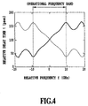
- Fig. 4 is a diagram showing a calculated characteristic example of the lattice-form optical circuit shown in Fig. 2.
- a delay time was derived by calculating a transfer function of the lattice-form optical circuit and obtaining the derivative of an imaginary part of the function with respect to an angular frequency.
- This calculated example shows a case where optical path length differences of the asymmetrical Mach-Zehnder interferometers are 4.276 mm, 7.483 mm, 7.483 mm, 7.483 mm, and 3.207 mm in the direction of the right in Fig. 2, and a refractive index of the waveguide is 1.45.
- the calculated result shows that the obtained dispersion values using the foregoing parameters are 830 psec/nm and -830 psec/nm.
- a different dispersion value can be obtained by changing the optical path length differences of the asymmetrical Mach-Zehnder interferometers.
- the optical path length difference is made L times
- the operational bandwidth and the delay time is made 1/L and L times, respectively, then the dispersion value is made L 2 times.
- each lattice-form optical circuits 4-1 to 4-N can be designed so as to have a dispersion compensation value corresponding to each channel wavelength.
- Control parts of waveguide refractive index 9a to 9e can be driven, for example, by using a thermo-optic or an electro-optic effect when using a glass or a dielectric waveguide, respectively.
- thermo-optic or an electro-optic effect when using a glass or a dielectric waveguide, respectively.
- semipermanent phase shift can be achieved without electrical power, by applying a local heating and quenching with high electrical power for a photoelastic effect to the control parts of waveguide refractive index 9a to 9e.
- dispersion compensation can be achieved without electrical power using the configuration in Fig. 2 and, consequently, using that in Fig. 1.
- Fig. 5 shows another configuration example of the directional couplers 8a to 8f in Fig. 2, which are composed of symmetrical Mach-Zehnder interferometer.
- Numerals 11a to 11f, 12a and 12b, and 13 represent waveguides (waveguides 11a and 11b, and 11 e and 11f are inputs and outputs, respectively), directional couplers (two waveguides are made approached each other), and a control part of waveguide refractive index, respectively. It is also possible to replace the directional couplers 12a and 12b with MMI-type couplers.
- the coupling coefficient can be arbitrarily varied from 0 and 1 by utilizing the interferometer's switching characteristic. It is also possible to replace the single symmetrical Mach-Zehnder interferometer in Fig. 5 with Mach-Zehnder interferometers cascaded in series.
- Fig. 6 is a diagram showing a calculated example of the group delay characteristic of the lattice-form optical circuit in Fig. 2 when the directional coupler in Fig. 5 is used.
- a delay time was derived by calculating a transfer function of the lattice-form optical circuit and obtaining the derivative of an imaginary part of the function with respect to an angular frequency.
- the arbitrary dispersion value ranging from -584 psec/nm to 584 psec/nm can be achieved using the foregoing parameters.
- the coupling coefficient of the directional coupler can be arbitrarily varied in the range of 0 to 1, dispersion of various values with both signs can be achieved. This is different from the case shown in Fig.4 where the coupling coefficient of the directional coupler is fixed.
- the lattice-form circuits 4-1 to 4-N having the following merits can be achieved. It is possible, by the single and compact circuit configuration, to adaptively compensate for the dispersion of various WDM signals, the dispersion of various fiber transmission lines having various dispersion values, and variation of dispersion value caused by the temperature change or the like.
- the configuration of the present embodiment in Fig. 1 can be used for the in-line dispersion slope equalizer.
- the dispersion slope equalizer is set in front of the transmission line, it is not necessary to demultiplex the wavelength division multiplexed signals.
- various wavelength signals modulated by the data patterns are introduced into the waveguides 3-1 to 3-N, and are transmitted into the fiber after pre-dispersion slope compensation and wavelength multiplexing. Therefore, in such an application, the wavelength demultiplexer 2 can be omitted in Fig. 7.
- the dispersion slope equalizer when the dispersion slope equalizer is set behind the transmission line, it is not necessary to multiplex demultiplexed signals again.
- photo detectors are connected to just behind the lattice-form optical circuits 4-1 to 4-N. Therefore, in such an application, the wavelength multiplexer 5 can be omitted in Fig. 8.
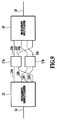
- Fig. 9 is a diagram showing the configuration of a second embodiment of the dispersion slope equalizer according to the present invention.
- the dispersion slope equalizer of the present embodiment comprises an input waveguide 14, a wavelength demultiplexer 15, waveguides 16a to 16h, lattice-form optical circuits 17a and 17b, a wavelength multiplexer 18, and an output waveguide 19.
- Both of the waveguides 7a and 7b in Fig. 2 and two of the waveguides 16a to 16d, and both of the waveguides 7e and 7f and two of the waveguides 16e to 16h are connected.
- wavelengths ⁇ 1 and ⁇ 4 or ⁇ 2 and ⁇ 3 are symmetrically set around the zero dispersion wavelength ⁇ 0.
- the dispersion values of ⁇ 1 and ⁇ 4 or ⁇ 2 and ⁇ 3 have the almost same absolute values with opposite sign each other. Therefore, one of two lattice-form optical circuits can be used for dispersion compensation of wavelength ⁇ 1 and ⁇ 4 signals, and the other for wavelength ⁇ 2 and ⁇ 3 signals.
- the number of lattice-form optical circuits must be four in the configuration in Fig. 1, but its number can be cut down by half by using the configuration in Fig. 9.
- the number of devices can be decreased to 3.
- Fig. 11 is a diagram showing a configuration in which the wavelength demultiplexer and multiplexer of the dispersion slope equalizer in Fig. 1 are composed of arrayed-waveguide gratings and all components are monolithically integrated on one substrate.
- First arrayed-waveguide grating demultiplexer 2a (AWG 1), second arrayed-waveguide grating multiplexer 5a (AWG 2) and an array of lattice-form optical circuits 50 (50-1 to 50-N) are integrated on a substrate 51a.
- Fig. 12 is a diagram showing a configuration in which the wavelength multiplexer of the dispersion slope equalizer in Fig. 7 is composed of an arrayed-waveguide grating and all components are monolithically integrated on one substrate.
- An arrayed-waveguide grating multiplexer 5a (AWG) and an array of the lattice-form optical circuits 50 (50-1 to 50-N) are integrated on one substrate 51b.
- the configuration in Fig. 12 is used when the dispersion slope equalizer is set in front of the transmission line. In this case, various wavelength signals from the transmitters are pre-dispersion slope compensated by the lattice-form optical circuits, and are transmitted into the fiber after wavelength multiplexing at the arrayed-waveguide grating 5a.
- the arrayed-waveguide grating demultiplexer 2a can be omitted in Fig. 12. Also in this case, by monolithically integrating all components on one substrate as shown in Fig. 12, uniformity of waveguide parameters are improved, and thus control of waveguide refractive index or the like become easy.
- Fig. 13 is a diagram showing a configuration in which the wavelength demultiplexer of the dispersion slope equalizer in Fig. 8 is composed of an arrayed-waveguide grating and all components are monolithically integrated on one substrate.
- First arrayed-waveguide grating demultiplexer 2a (AWG) and an array of the lattice-form optical circuits 50 (50-1 to 50-N) are integrated on the substrate 51c.
- the configuration in Fig. 13 is used when the dispersion slope equalizer is set behind the transmission line. In this case, it is not necessary to multiplex demultiplexed signals again. Therefore, the arrayed-waveguide grating multiplexer 5a can be omitted in Fig. 13. Also in this case, by monolithically integrating all components on one substrate as shown in Fig. 13, uniformity of waveguide parameters are improved, and thus control of waveguide refractive index or the like become easy.
- Fig. 14 is a diagram showing the configuration of a third embodiment of the dispersion slope equalizer according to the present invention.
- the dispersion slope equalizer of the present embodiment comprises an input waveguide 20, a wavelength demultiplexer 21, waveguides 22-1 to 22-N, transversal-form optical circuits 23-1 to 23-N, a wavelength multiplexer 24, and an output waveguide 25.
- Fig. 15 is a diagram showing a configuration example of the transversal-form optical circuits 23-1 to 23-N.
- the transversal-form optical circuits 23-1 to 23-N have the following configuration.
- the lightwaves are introduced into the input waveguide 26a or 26b, and then are tapped at eight taps 27a to 27h, and are finally multiplexed again by the multiplexer 29 into the output waveguide 30.
- Numerals 26a to 26i and 28a to 28h are waveguides and waveguide control parts of refractive index, respectively.
- One of the waveguides 26a and 26b and the output waveguide 30 are connected to one of the waveguides 22-1 to 22-N in Fig. 14.
- MMI-type couplers or directional couplers shown in Fig. 5 can be used as taps 27a to 27h.
- Star coupler, an MMI-type coupler, 2 x 2 directional couplers cascaded in series, or Y-branching waveguides cascaded in series can be used as the multiplexer 29.
- the group delay time can be approximated by an arbitrary shape function with respect to an optional frequency (see, for example, K. Sasayama et al., "Coherent optical transversal filter using silica-based waveguides for high-speed signal processing," Journal of Lightwave Technology, vol.9, no.10, pp. 1225-1230, October 1991). Therefore, it is also possible to obtain the characteristics in Figs. 4 and 6 by using the configuration in the present embodiment.
- the single and compact equalizer configuration in the present embodiment to adaptively compensate for the dispersion of various fiber transmission lines having various dispersion values and variation of dispersion value caused by the temperature change or the like.
- the configuration of the present embodiment in Fig. 14 can be used for the in-line dispersion slope equalizer.
- the dispersion slope equalizer is set in front of the transmission line, it is not necessary to demultiplex the wavelength division multiplexed signals.
- various wavelength signals modulated by the data patterns are introduced into the waveguides 22-1 to 22-N, and are transmitted into the fiber after pre-dispersion slope compensation and wavelength multiplexing. Therefore, in such an application, the wavelength demultiplexer 21 can be omitted in Fig. 16.
- the dispersion slope equalizer when the dispersion slope equalizer is set behind the transmission line, it is not necessary to multiplex demultiplexed signals again.
- photo detectors are connected to just behind the transversal-form optical circuits 23-1 to 23-N. Therefore, in such an application, the wavelength multiplexer 24 can be omitted in Fig. 17.
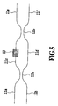
- Fig. 18 is a diagram showing the configuration of a fourth embodiment of the dispersion slope equalizer according to the present invention.
- the dispersion slope equalizer of the present embodiment comprises an input waveguide 31, arrayed-waveguide gratings 37a and 37b, waveguides 34a to 34d, lattice-form or transversal-form optical circuits, or the like 35a to 35d, and an output waveguide 36.
- the arrayed-waveguide gratings 37a and 37b comprise slab waveguides 32a to 32d and arrayed-waveguides 33a and 33b.
- Fig. 18 shows a case where the wavelength demultiplexers 2, 15, and 21 and the wavelength multiplexers 5, 18, and 24 of the dispersion slope equalizer in Figs. 1, 9 and 14 are composed of arrayed-waveguide gratings.
- elements 35a to 35d with the lattice-form optical circuits in Fig. 2, the transversal-form optical circuits in Fig. 15, or the combination of these two circuits, a perfectly integrated dispersion slope equalizer can be achieved.
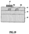
- the waveguides of the dispersion slope equalizer in the foregoing embodiments according to the present invention can be formed by using silica glass waveguides 40a and 40b as shown in Fig. 19.
- Fig. 19 is a sectional diagram of the waveguide, and a waveguide fabrication procedure in first to fourth embodiments will be described by referring to the drawing.
- a SiO 2 under cladding layer 39 is deposited on a Si substrate 38 by a flame hydrolysis deposition method.
- a SiO 2 glass core layer mixed with dopant GeO 2 is deposited on the SiO 2 under cladding layer 39, consolidation is carried out using an electrical furnace.
- cores (silica waveguide) 40a and 40b are formed.
- a SiO 2 upper cladding layer 41 is deposited again on the SiO 2 under cladding layer 39 on which the cores 40a and 40b are formed, and consolidation is carried out again by the electrical furnace.
- thin film heaters 42 and metal interconnection are formed on some optical waveguides by an evaporation.
- the thin film heaters 42 can be used to carry out phase control of waveguides by thermo-optic effect.
- the waveguides forming the dispersion slope equalizer according to the present invention are not restricted to the glass waveguides, and it is obvious that dielectric waveguides, semiconductor waveguides, polymer waveguides, and optical fibers or the like can be applicable to the equalizer. Further, it is also obvious that the equalizer can be realized by hybrid-integrating several types of waveguides.
Abstract
Description
- The present invention is on a dispersion slope equalizer that simultaneously recovers waveforms of wavelength division multiplexed (WDM) signals distorted by dispersion characteristic (that is; group delay is different at each wavelength) in an optical fiber.
- Today, the investigation to achieve a large capacity optical transmission systems is being actively carried out utilizing a dispersion shifted fiber (DSF) having zero dispersion or a non-zero dispersion shifted fiber (NZ-DSF) having several psec/nm/km dispersion at wavelength λ = 1.55 µm band.
- However, when WDM transmission using DSF's is carried out in order to realize large capacity networks, second-order dispersion (derivative of group delay with respect to wavelength) is different at each wavelength channel as shown in Fig. 20 (relative delay time characteristics of DSF). This dispersion difference is caused by dispersion slope, namely, third-order dispersion (derivative of second-order dispersion with respect to wavelength), whose typical value is about 0.07 psec/nm2/km. As a result, the signal pulse at each wavelength channel is differently distorted, which limits (distance between repeaters). This is also the same as when NZ-DSF is used.
- Up to now, configuration in Fig. 21 has been known as a dispersion slope equalizer, which recovers the distorted waveforms of WDM signals by the dispersion in fibers. In Fig. 21, dispersion compensating fiber (DCF) 44 is set behind
fiber transmission line 43. In this configuration, dispersion characteristic in the fiber transmission line can be compensated by the DCF, whose dispersion has the same absolute value with opposite sign to that of the fiber transmission line. - However, the prior art dispersion slope equalizer having the foregoing configuration has following problems:
- (1) by utilizing the foregoing configuration, it is possible to compensate for dispersion slope of a 1.3 µm band zero dispersion fiber (that is; single mode fiber (SMF)) at 1.55 µm band, but it is impossible to compensate for dispersion slope of DSF or NZ-DSF at 1.55 µm band,
- (2) configuration is complicated and the size is large, and
- (3) compensation value is fixed, and it is impossible to compensate for the dispersion of various fiber transmission lines having various dispersion values and variation of dispersion value caused by the temperature change or the like by utilizing the foregoing configuration.
-
- Considering the foregoing problems, an object of the present invention is to provide a compact dispersion slope equalizer by which it is possible to simultaneously recover distorted waveforms of WDM signals by dispersion slope of DSF or NZ-DSF at 1.55 µm band, and to compensate for the dispersion of various fiber transmission lines having various dispersion values and variation of dispersion value caused by the temperature change or the like. This configuration comprises group delay controllers comprising lattice-form optical circuits, transversal-form optical circuits, or the combination of these two circuits.
- To realize the foregoing object, according to a 1st aspect of the present invention, there is provided a dispersion slope equalizer for compensating signal distortion caused by dispersion slope of a transmission line when transmitting lightwaves with plural wavelength signals in the transmission line characterized by comprising: N (N: natural number) waveguides, N output wavelength demultiplexer and/or N input wavelength multiplexer, and K (K: natural number, K≦N) group delay controllers; the N waveguides being connected to outputs of the wavelength demultiplexer and/or inputs of the wavelength multiplexer; in the group delay controllers, one or both of input/output parts of lattice-form optical circuits being set on the N waveguides; wherein the lattice-form optical circuits are composed of two waveguides interleaved with at least two directional couplers, and the two waveguides are designed so that optical path lengths between the directional couplers are different.
- According to a 2nd aspect of the invention, the wavelength demultiplexer and the wavelength multiplexer are arrayed-waveguide gratings.
- According to a 3rd aspect of the invention, the group delay controllers are connected to N input wavelength multiplexer and the N waveguides are connected to only inputs of the wavelength multiplexer.
- According to a 4th aspect of the invention, the wavelength multiplexer is an arrayed-waveguide grating.
- According to a 5th aspect of the invention, the group delay controllers are connected to N output wavelength demultiplexer and the N waveguides are connected to only outputs of the wavelength demultiplexer.
- According to a 6th aspect of the invention, the wavelength demultiplexer is an arrayed-waveguide grating.
- According to a 7th aspect of the invention, the group delay controllers are composed of the combination of the lattice-form and transversal-form optical circuits.
- According to an 8th aspect of the invention, there is provided a dispersion slope equalizer for compensating signal distortion caused by dispersion slope of a transmission line when transmitting lightwaves with plural wavelength signals in the transmission line characterized by comprising: N (N: natural number) waveguides, N output wavelength demultiplexer and/or N input wavelength multiplexer, and N group delay controllers; the N waveguides being connected to outputs of the wavelength demultiplexer and/or inputs of the wavelength multiplexer; in the group delay controllers, one of inputs and an output of transversal-form optical circuits being set on the N waveguides; wherein the transversal-form optical circuit is provided with first waveguide for one of inputs and M (M: natural number, M≧2)directional couplers for coupling M waveguides with the first waveguide at M different positions, and the M waveguides, after being coupled with the first waveguide, are multiplexed by a multiplexer into second output waveguide.
- According to a 9th aspect of the invention, the wavelength demultiplexer and the wavelength multiplexer are arrayed-waveguide gratings.
- According to a 10th aspect of the invention, the group delay controllers are connected to N input wavelength multiplexer and the N waveguides are connected to only inputs of the wavelength multiplexer.
- According to an 11th aspect of the invention, the wavelength multiplexer is an arrayed-waveguide grating.
- According to a 12th aspect of the invention, the group delay controllers are connected to N outputs wavelength demultiplexer and the N waveguides are connected to only outputs of the wavelength demultiplexer.
- According to a 13th aspect of the invention, the wavelength demultiplexer is an arrayed-waveguide grating.
- According to a 14th aspect of the invention, the group delay controllers are composed of the combination of the transversal-form and lattice-form optical circuits.
- The dispersion slope equalizer according to the present invention comprises integrated-optic components, that is; a wavelength demultiplexer and/or a wavelength multiplexer and a lattice-form optical circuit and/or a transversal-form optical circuit. By using this compact configuration, it is possible to compensate for the dispersion of various fiber transmission lines having various dispersion values and variation of dispersion value caused by the temperature change or the like, and to simultaneously recover distorted waveforms of WDM signals by dispersion slope of DSF or NZ-DSF at 1.55 µm band.
- The foregoing and other objects, effects, features and advantages in the present invention will become more apparent by showing the following description of embodiments with the accompanying drawings.
- Fig. 1 is a diagram showing the configuration of a first embodiment of the dispersion slope equalizer according to the present invention;
- Fig. 2 is a diagram showing the configuration of a lattice-form optical circuit shown in Fig. 1;
- Fig. 3 is a diagram showing a configuration example of a directional coupler shown in Fig. 2;
- Fig. 4 is a diagram showing a calculated characteristic example of the lattice-form optical circuit shown in Fig. 2;
- Fig. 5 is a diagram showing another configuration example of the directional coupler shown in Fig. 2;
- Fig. 6 is a diagram showing another calculated characteristic example of the lattice-form optical circuit shown in Fig. 2;
- Fig. 7 is a diagram for explaining a case where the dispersion slope equalizer is set in front of a transmission line;
- Fig. 8 is a diagram for explaining a case where the dispersion slope equalizer is set behind a transmission line;
- Fig. 9 is a diagram showing the configuration of a second embodiment of the dispersion slope equalizer according to the present invention;
- Fig. 10 is a diagram showing a group delay characteristic example of an optical fiber;
- Fig. 11 is a diagram showing a configuration in which the wavelength demultiplexer and multiplexer of the dispersion slope equalizer in Fig. 1 are composed of arrayed-waveguide gratings and all components of the dispersion slope equalizer are monolithically integrated on one substrate;
- Fig. 12 is a diagram showing a configuration in which the wavelength multiplexer of the dispersion slope equalizer in Fig. 7 is composed of an arrayed-waveguide grating and all components of the dispersion slope equalizer are monolithically integrated on one substrate;
- Fig. 13 is a diagram showing a configuration in which the wavelength demultiplexer of the dispersion slope equalizer in Fig. 8 is composed of an arrayed-waveguide grating and all components of the dispersion slope equalizer are monolithically integrated on one substrate;
- Fig. 14 is a diagram showing the configuration of a third embodiment of the dispersion slope equalizer according to the present invention;
- Fig. 15 is a diagram showing a configuration example of the transversal-form optical circuit shown in Fig. 14;
- Fig. 16 is a diagram for explaining a case where the dispersion slope equalizer is set in front of a transmission line;
- Fig. 17 is a diagram for explaining a case where the dispersion slope equalizer is set behind a transmission line;
- Fig. 18 is a diagram showing the configuration of a fourth embodiment of the dispersion slope equalizer according to the present invention;
- Fig. 19 is a diagram showing the sectional structure of a silica glass waveguide used in the first to fourth embodiments;
- Fig. 20 is a diagram showing an example of group delay characteristic of an optical fiber; and
- Fig. 21 is a diagram showing a configuration example of a prior art dispersion slope equalizer.
-
- Fig. 1 is a diagram showing the configuration of a first embodiment of the dispersion slope equalizer according to the present invention;
- In Fig. 1, the dispersion slope equalizer of the present embodiment comprises an input waveguide 1, a
wavelength demultiplexer 2, waveguides 3-1 to 3-N, lattice-form optical circuits 4-1 to 4-N, awavelength multiplexer 5, and anoutput waveguide 6. - WDM signal lightwaves λ1 to λN distorted by the dispersion slope are introduced into the input waveguide 1 and are demultiplexed by the
wavelength demultiplexer 2 into wavelength components. Then, these wavelength components are introduced into the lattice-form optical circuits 4-1 to 4-N for dispersion slope compensation, and are multiplexed by thewavelength multiplexer 5. Finally, the multiplexed lightwaves are outputted at theoutput waveguide 6, thus achieving the dispersion slope equalizer. - The
wavelength demultiplexer 2 and thewavelength multiplexer 5 can be composed of not only arrayed-waveguide gratings (described in detail later), but also cascaded configuration of Mach-Zehnder interferometers, bulk-type optical filters, or fiber-type (or waveguide-type) gratings in series. - Fig. 2 is a diagram showing a configuration example of the lattice-form optical circuits 4-1 to 4-N.
- This lattice-form optical circuit has a configuration in which five asymmetrical arm pairs are cascaded in series by setting six directional couplers, that is; asymmetrical Mach-Zehnder interferometers are cascaded in series. In Fig. 2, 7a to 7f are waveguides (
waveguides - Four lattice-form optical circuits 4-1 to 4-N in Fig. 1 are connected to one of waveguides 3-1 to 3-N by utilizing one of the
waveguides waveguides 7e and 7f. - The
directional couplers 8a to 8f can have a configuration in which the twowaveguides refractive index 9a to 9e, it is possible to make higher frequency lightwaves pass through a longer or shorter optical path length in Fig. 2. Therefore, a dispersion equalizer can be achieved whose group delay increases or decreases with increase of frequency. - Fig. 4 is a diagram showing a calculated characteristic example of the lattice-form optical circuit shown in Fig. 2. Here, a delay time was derived by calculating a transfer function of the lattice-form optical circuit and obtaining the derivative of an imaginary part of the function with respect to an angular frequency.
- This calculated example shows a case where optical path length differences of the asymmetrical Mach-Zehnder interferometers are 4.276 mm, 7.483 mm, 7.483 mm, 7.483 mm, and 3.207 mm in the direction of the right in Fig. 2, and a refractive index of the waveguide is 1.45.
- The calculated result shows that the obtained dispersion values using the foregoing parameters are 830 psec/nm and -830 psec/nm.
- A different dispersion value can be obtained by changing the optical path length differences of the asymmetrical Mach-Zehnder interferometers. When the optical path length difference is made L times, the operational bandwidth and the delay time is made 1/L and L times, respectively, then the dispersion value is made L2 times.
- Also, when the cascade number of the asymmetrical Mach-Zehnder interferometers is increased or decreased, absolute value of the dispersion can be increased or decreased, respectively. This is because that the delay time is increased or decreased by increasing or decreasing the total optical path length difference, respectively.
- Thus, each lattice-form optical circuits 4-1 to 4-N can be designed so as to have a dispersion compensation value corresponding to each channel wavelength.
- Control parts of waveguide
refractive index 9a to 9e can be driven, for example, by using a thermo-optic or an electro-optic effect when using a glass or a dielectric waveguide, respectively. Also, when a glass waveguide is used, semipermanent phase shift can be achieved without electrical power, by applying a local heating and quenching with high electrical power for a photoelastic effect to the control parts of waveguiderefractive index 9a to 9e. Thus, dispersion compensation can be achieved without electrical power using the configuration in Fig. 2 and, consequently, using that in Fig. 1. - Fig. 5 shows another configuration example of the
directional couplers 8a to 8f in Fig. 2, which are composed of symmetrical Mach-Zehnder interferometer. - Numerals 11a to 11f, 12a and 12b, and 13 represent waveguides (
waveguides directional couplers - When the phase in control part of the waveguide
refractive index 13 is changed from 0 to 2p, the coupling coefficient can be arbitrarily varied from 0 and 1 by utilizing the interferometer's switching characteristic. It is also possible to replace the single symmetrical Mach-Zehnder interferometer in Fig. 5 with Mach-Zehnder interferometers cascaded in series. - By appropriately tuning coupling coefficients of the
directional couplers 8a to 8f and the waveguide phase in the control parts of waveguiderefractive index 9a to 9e, it is possible to achieve a dispersion equalizer whose group delay can be varied to various values with both signs with respect to frequency. - Fig. 6 is a diagram showing a calculated example of the group delay characteristic of the lattice-form optical circuit in Fig. 2 when the directional coupler in Fig. 5 is used.
- Here, a case is shown where the number of the asymmetrical Mach-Zehnder interferometers is 6, optical path length differences in the all asymmetrical Mach-Zehnder interferometers are 2.759 mm, and waveguide refractive index is 1.45. Also in this case, a delay time was derived by calculating a transfer function of the lattice-form optical circuit and obtaining the derivative of an imaginary part of the function with respect to an angular frequency.
- It is shown, by appropriately tuning coupling coefficients of the
directional couplers 8a to 8f and the waveguide phase in the control parts of waveguiderefractive index 9a to 9e, the arbitrary dispersion value ranging from -584 psec/nm to 584 psec/nm can be achieved using the foregoing parameters. - In this case, as the coupling coefficient of the directional coupler can be arbitrarily varied in the range of 0 to 1, dispersion of various values with both signs can be achieved. This is different from the case shown in Fig.4 where the coupling coefficient of the directional coupler is fixed.
- By using the
directional couplers 8a to 8f in the configuration of Fig. 5, the lattice-form circuits 4-1 to 4-N having the following merits can be achieved. It is possible, by the single and compact circuit configuration, to adaptively compensate for the dispersion of various WDM signals, the dispersion of various fiber transmission lines having various dispersion values, and variation of dispersion value caused by the temperature change or the like. - Also as described before, when a glass waveguide is used, semipermanent phase shift can be achieved without electrical power, by carrying out a local heating and quenching with high electrical power for a photoelastic effect. Thus, dispersion compensation can be achieved without electrical power using the configuration in Fig. 2 and, consequently, using that in Fig. 1.
- The configuration of the present embodiment in Fig. 1 can be used for the in-line dispersion slope equalizer. When the dispersion slope equalizer is set in front of the transmission line, it is not necessary to demultiplex the wavelength division multiplexed signals. In this case, various wavelength signals modulated by the data patterns are introduced into the waveguides 3-1 to 3-N, and are transmitted into the fiber after pre-dispersion slope compensation and wavelength multiplexing. Therefore, in such an application, the
wavelength demultiplexer 2 can be omitted in Fig. 7. - On the other hand, when the dispersion slope equalizer is set behind the transmission line, it is not necessary to multiplex demultiplexed signals again. In this case, photo detectors are connected to just behind the lattice-form optical circuits 4-1 to 4-N. Therefore, in such an application, the
wavelength multiplexer 5 can be omitted in Fig. 8. - The elements 4-1 to 4-N in Figs. 1, 7, and 8 can be replaced with the combination of lattice-form and transversal-form optical circuits.
- Fig. 9 is a diagram showing the configuration of a second embodiment of the dispersion slope equalizer according to the present invention.
- In Fig. 9, the dispersion slope equalizer of the present embodiment comprises an
input waveguide 14, awavelength demultiplexer 15,waveguides 16a to 16h, lattice-formoptical circuits wavelength multiplexer 18, and anoutput waveguide 19. Both of thewaveguides waveguides 16a to 16d, and both of thewaveguides 7e and 7f and two of thewaveguides 16e to 16h are connected. - In the lattice-form optical circuits in Fig. 2, it is confirmed that dispersion characteristic between two sets of input/output ports, for example, dispersion characteristics between the
input waveguide 7a and theoutput waveguide 7e and between theinput waveguide 7b and the output waveguide 7f have the same absolute value with opposite sign. This was confirmed because a transfer matrix of the lattice-form optical circuit shows unitary. - As shown in Fig. 10, wavelengths λ1 and λ4 or λ2 and λ3 are symmetrically set around the zero dispersion wavelength λ0. The dispersion values of λ1 and λ4 or λ2 and λ3 have the almost same absolute values with opposite sign each other. Therefore, one of two lattice-form optical circuits can be used for dispersion compensation of wavelength λ1 and λ4 signals, and the other for wavelength λ2 and λ3 signals.
- When dispersion compensation for 4 wavelength signals is carried out, for example, the number of lattice-form optical circuits must be four in the configuration in Fig. 1, but its number can be cut down by half by using the configuration in Fig. 9.
- By replacing one lattice-form
optical circuit 17b with two transversal-form optical circuits, and connectingwaveguide 16b, transversal-form optical circuit A, andwaveguide 16g, andwaveguide 16c, transversal-form optical circuit B, andwaveguide 16h, the number of devices can be decreased to 3. - Fig. 11 is a diagram showing a configuration in which the wavelength demultiplexer and multiplexer of the dispersion slope equalizer in Fig. 1 are composed of arrayed-waveguide gratings and all components are monolithically integrated on one substrate. First arrayed-waveguide
grating demultiplexer 2a (AWG 1), second arrayed-waveguidegrating multiplexer 5a (AWG 2) and an array of lattice-form optical circuits 50 (50-1 to 50-N) are integrated on asubstrate 51a. - By monolithically integrating all components on one substrate as shown in Fig. 11, uniformity of waveguide parameters are improved, and thus control of waveguide refractive index or the like become easy. Further, production process and packaging of the device are made easy, and the device size is reduced. On the other hand, it is possible to connect separately prepared substrate(s) with lattice-form optical circuit(s) to arrayed-waveguide gratings using an optical fiber or the like.
- Fig. 12 is a diagram showing a configuration in which the wavelength multiplexer of the dispersion slope equalizer in Fig. 7 is composed of an arrayed-waveguide grating and all components are monolithically integrated on one substrate. An arrayed-waveguide
grating multiplexer 5a (AWG) and an array of the lattice-form optical circuits 50 (50-1 to 50-N) are integrated on onesubstrate 51b. The configuration in Fig. 12 is used when the dispersion slope equalizer is set in front of the transmission line. In this case, various wavelength signals from the transmitters are pre-dispersion slope compensated by the lattice-form optical circuits, and are transmitted into the fiber after wavelength multiplexing at the arrayed-waveguide grating 5a. Therefore, the arrayed-waveguidegrating demultiplexer 2a can be omitted in Fig. 12. Also in this case, by monolithically integrating all components on one substrate as shown in Fig. 12, uniformity of waveguide parameters are improved, and thus control of waveguide refractive index or the like become easy. - Fig. 13 is a diagram showing a configuration in which the wavelength demultiplexer of the dispersion slope equalizer in Fig. 8 is composed of an arrayed-waveguide grating and all components are monolithically integrated on one substrate. First arrayed-waveguide
grating demultiplexer 2a (AWG) and an array of the lattice-form optical circuits 50 (50-1 to 50-N) are integrated on thesubstrate 51c. The configuration in Fig. 13 is used when the dispersion slope equalizer is set behind the transmission line. In this case, it is not necessary to multiplex demultiplexed signals again. Therefore, the arrayed-waveguidegrating multiplexer 5a can be omitted in Fig. 13. Also in this case, by monolithically integrating all components on one substrate as shown in Fig. 13, uniformity of waveguide parameters are improved, and thus control of waveguide refractive index or the like become easy. - In the embodiments in Fig. 11 to Fig. 13, a case, where only an array of the lattice-form optical circuits is used as the dispersion slope equalizer, is described. Also, an array of the transversal-form optical circuits and the combination of the lattice-form and transversal-form optical circuits can be used as the dispersion slope equalizer.
- Fig. 14 is a diagram showing the configuration of a third embodiment of the dispersion slope equalizer according to the present invention.
- In Fig. 14, the dispersion slope equalizer of the present embodiment comprises an
input waveguide 20, awavelength demultiplexer 21, waveguides 22-1 to 22-N, transversal-form optical circuits 23-1 to 23-N, awavelength multiplexer 24, and anoutput waveguide 25. - Fig. 15 is a diagram showing a configuration example of the transversal-form optical circuits 23-1 to 23-N.
- The transversal-form optical circuits 23-1 to 23-N have the following configuration. The lightwaves are introduced into the
input waveguide taps 27a to 27h, and are finally multiplexed again by themultiplexer 29 into theoutput waveguide 30. Numerals 26a to 26i and 28a to 28h are waveguides and waveguide control parts of refractive index, respectively. One of thewaveguides output waveguide 30 are connected to one of the waveguides 22-1 to 22-N in Fig. 14. - Directional couplers shown in Fig. 3, MMI-type couplers or directional couplers shown in Fig. 5 can be used as
taps 27a to 27h. Star coupler, an MMI-type coupler, 2 x 2 directional couplers cascaded in series, or Y-branching waveguides cascaded in series can be used as themultiplexer 29. - In Fig. 15, by appropriately tuning the coupling coefficient of the
taps 27a to 27h and the waveguide phase in the control parts of waveguiderefractive index 28a to 28h, the characteristic between thewaveguide 26a and theoutput waveguide 30 or between thewaveguide 26b and theoutput waveguide 30, the group delay time can be approximated by an arbitrary shape function with respect to an optional frequency (see, for example, K. Sasayama et al., "Coherent optical transversal filter using silica-based waveguides for high-speed signal processing," Journal of Lightwave Technology, vol.9, no.10, pp. 1225-1230, October 1991). Therefore, it is also possible to obtain the characteristics in Figs. 4 and 6 by using the configuration in the present embodiment. - Therefore, dispersion slope compensation for WDM signals is also possible by using the configuration in Fig. 14.
- It is possible, by the single and compact equalizer configuration in the present embodiment, to adaptively compensate for the dispersion of various fiber transmission lines having various dispersion values and variation of dispersion value caused by the temperature change or the like.
- Also as described before, when a glass waveguide is used, semipermanent phase shift can be achieved without electrical power, by carrying out a local heating and quenching with high electrical power for a photoelastic effect. Thus, dispersion compensation can be achieved without electrical power using the configuration in Fig. 14.
- The configuration of the present embodiment in Fig. 14 can be used for the in-line dispersion slope equalizer. When the dispersion slope equalizer is set in front of the transmission line, it is not necessary to demultiplex the wavelength division multiplexed signals. In this case, various wavelength signals modulated by the data patterns are introduced into the waveguides 22-1 to 22-N, and are transmitted into the fiber after pre-dispersion slope compensation and wavelength multiplexing. Therefore, in such an application, the
wavelength demultiplexer 21 can be omitted in Fig. 16. - On the other hand, when the dispersion slope equalizer is set behind the transmission line, it is not necessary to multiplex demultiplexed signals again. In this case, photo detectors are connected to just behind the transversal-form optical circuits 23-1 to 23-N. Therefore, in such an application, the
wavelength multiplexer 24 can be omitted in Fig. 17. - Fig. 18 is a diagram showing the configuration of a fourth embodiment of the dispersion slope equalizer according to the present invention.
- In Fig. 18, the dispersion slope equalizer of the present embodiment comprises an
input waveguide 31, arrayed-waveguide gratings waveguides 34a to 34d, lattice-form or transversal-form optical circuits, or the like 35a to 35d, and anoutput waveguide 36. The arrayed-waveguide gratings slab waveguides 32a to 32d and arrayed-waveguides - The configuration of Fig. 18 shows a case where the
wavelength demultiplexers wavelength multiplexers elements 35a to 35d with the lattice-form optical circuits in Fig. 2, the transversal-form optical circuits in Fig. 15, or the combination of these two circuits, a perfectly integrated dispersion slope equalizer can be achieved. - The waveguides of the dispersion slope equalizer in the foregoing embodiments according to the present invention can be formed by using
silica glass waveguides - Fig. 19 is a sectional diagram of the waveguide, and a waveguide fabrication procedure in first to fourth embodiments will be described by referring to the drawing.
- First, a SiO2 under
cladding layer 39 is deposited on aSi substrate 38 by a flame hydrolysis deposition method. Next, after a SiO2 glass core layer mixed with dopant GeO2 is deposited on the SiO2 undercladding layer 39, consolidation is carried out using an electrical furnace. - Then, by etching the core layer using patterns shown in Figs. 1 to 3, Fig. 5, Figs. 7 to 9, and Figs. 11 to 18, cores (silica waveguide) 40a and 40b are formed.
- Next, a SiO2
upper cladding layer 41 is deposited again on the SiO2 undercladding layer 39 on which thecores thin film heaters 42 and metal interconnection are formed on some optical waveguides by an evaporation. - In the dispersion slope equalizers in first to fourth embodiments whose waveguides are formed by the foregoing method, the
thin film heaters 42 can be used to carry out phase control of waveguides by thermo-optic effect. - The waveguides forming the dispersion slope equalizer according to the present invention are not restricted to the glass waveguides, and it is obvious that dielectric waveguides, semiconductor waveguides, polymer waveguides, and optical fibers or the like can be applicable to the equalizer. Further, it is also obvious that the equalizer can be realized by hybrid-integrating several types of waveguides.
- The present invention has been described in detail with respect to preferred embodiments, and it will now be apparent from the foregoing to those skilled in the art that changes and modifications may be made without departing from the invention in its broader aspects, and it is the intention, therefore, in the appended claims to cover all such changes and modifications as fall within the true spirit of the invention.
Claims (14)
- A dispersion slope equalizer for compensating signal distortion caused by dispersion slope of a transmission line when transmitting lightwaves with plural wavelength signals in the transmission line characterized by comprising:N (N: natural number) waveguides, N output wavelength demultiplexer and/or N input wavelength multiplexer, and K (K: natural number, K≦N) group delay controllers;said N waveguides being connected to outputs of said wavelength demultiplexer and/or inputs of said wavelength multiplexer;in said group delay controllers, one or both of input/output parts of lattice-form optical circuits being set on said N waveguides;
wherein said lattice-form optical circuits are composed of two waveguides interleaved with at least two directional couplers, and said two waveguides are designed so that optical path lengths between said directional couplers are different. - The dispersion slope equalizer as claimed in Claim 1, characterized in that said wavelength demultiplexer and said wavelength multiplexer are arrayed-waveguide gratings.
- The dispersion slope equalizer as claimed in Claim 1, characterized in that said group delay controllers are connected to N input wavelength multiplexer and said N waveguides are connected to only inputs of said wavelength multiplexer.
- The dispersion slope equalizer as claimed in Claim 3, characterized in that said wavelength multiplexer is an arrayed-waveguide grating.
- The dispersion slope equalizer as claimed in Claim 1, characterized in that said group delay controllers are connected to N output wavelength demultiplexer and said N waveguides are connected to only outputs of said wavelength demultiplexer.
- The dispersion slope equalizer as claimed in Claim 5, characterized in that said wavelength demultiplexer is an arrayed-waveguide grating.
- The dispersion slope equalizer as claimed in Claim 1, characterized in that said group delay controllers are composed of the combination of the lattice-form and transversal-form optical circuits.
- A dispersion slope equalizer for compensating signal distortion caused by dispersion slope of a transmission line when transmitting lightwaves with plural wavelength signals in the transmission line characterized by comprising:N (N: natural number) waveguides, N output wavelength demultiplexer and/or N input wavelength multiplexer, and N group delay controllers;said N waveguides being connected to outputs of said wavelength demultiplexer and/or inputs of said wavelength multiplexer;in said group delay controllers, one of inputs and an output of transversal-form optical circuits being set on said N optical waveguides;
wherein the transversal-form optical circuit is provided with first waveguide for one of inputs and M (M: natural number, M≧2)directional couplers for coupling M waveguides with said first waveguide at M different positions, and said M waveguides, after being coupled with said first waveguide, are multiplexed by a multiplexer into a second output waveguide. - The dispersion slope equalizer as claimed in Claim 8, characterized in that said wavelength demultiplexer and said wavelength multiplexer are arrayed-waveguide gratings.
- The dispersion slope equalizer as claimed in Claim 8, characterized in that said group delay controllers are connected to N input wavelength multiplexer and said N waveguides are connected to only inputs of said wavelength multiplexer.
- The dispersion slope equalizer as claimed in Claim 10, characterized in that said wavelength multiplexer is an arrayed-waveguide grating.
- The dispersion slope equalizer as claimed in Claim 8, characterized in that said group delay controllers are connected to N output wavelength demultiplexer and said N waveguides are connected to only outputs of said wavelength demultiplexer.
- The dispersion slope equalizer as claimed in Claim 12, characterized in that said wavelength demultiplexer is an arrayed-waveguide grating.
- The dispersion slope equalizer as claimed in Claim 8, characterized in that said group delay controllers are composed of the combination of the transversal-form and lattice-form optical circuits.
Priority Applications (1)
| Application Number | Priority Date | Filing Date | Title |
|---|---|---|---|
| EP06076011A EP1689101A3 (en) | 1999-10-19 | 2000-10-18 | Dispersion slope equalizer |
Applications Claiming Priority (2)
| Application Number | Priority Date | Filing Date | Title |
|---|---|---|---|
| JP29687799 | 1999-10-19 | ||
| JP29687799 | 1999-10-19 |
Related Child Applications (2)
| Application Number | Title | Priority Date | Filing Date |
|---|---|---|---|
| EP06076011A Division EP1689101A3 (en) | 1999-10-19 | 2000-10-18 | Dispersion slope equalizer |
| EP06076011.3 Division-Into | 2006-05-08 |
Publications (3)
| Publication Number | Publication Date |
|---|---|
| EP1094625A2 true EP1094625A2 (en) | 2001-04-25 |
| EP1094625A3 EP1094625A3 (en) | 2004-01-02 |
| EP1094625B1 EP1094625B1 (en) | 2010-06-09 |
Family
ID=17839330
Family Applications (2)
| Application Number | Title | Priority Date | Filing Date |
|---|---|---|---|
| EP00309165A Expired - Lifetime EP1094625B1 (en) | 1999-10-19 | 2000-10-18 | Dispersion slope equalizer |
| EP06076011A Ceased EP1689101A3 (en) | 1999-10-19 | 2000-10-18 | Dispersion slope equalizer |
Family Applications After (1)
| Application Number | Title | Priority Date | Filing Date |
|---|---|---|---|
| EP06076011A Ceased EP1689101A3 (en) | 1999-10-19 | 2000-10-18 | Dispersion slope equalizer |
Country Status (3)
| Country | Link |
|---|---|
| US (2) | US6912362B1 (en) |
| EP (2) | EP1094625B1 (en) |
| DE (1) | DE60044523D1 (en) |
Cited By (1)
| Publication number | Priority date | Publication date | Assignee | Title |
|---|---|---|---|---|
| EP2405597A1 (en) * | 2009-03-06 | 2012-01-11 | Huawei Technologies Co., Ltd. | Method and device for dispersion slope compensation |
Families Citing this family (13)
| Publication number | Priority date | Publication date | Assignee | Title |
|---|---|---|---|---|
| US7171067B2 (en) * | 2003-03-03 | 2007-01-30 | Lucent Technologies Inc. | Integrateable optical interleaver and de-interleaver |
| US7747171B1 (en) * | 2002-09-10 | 2010-06-29 | Meriton Networks Us Inc. | Method and apparatus for alleviating slope-induced impairments to chirped optical signals propagating in an optical transmission system |
| EP1427120B1 (en) * | 2002-12-03 | 2005-02-09 | Alcatel | Polarization mode dispersion controller using feed-forward compensation |
| US7590312B2 (en) * | 2003-07-04 | 2009-09-15 | Nippon Telegraph And Telephone Corporation | Interferometer optical switch and variable optical attenuator |
| US7555220B2 (en) * | 2003-10-22 | 2009-06-30 | Infinera Corporation | Chromatic dispersion compensator (CDC) in a photonic integrated circuit (PIC) chip and method of operation |
| JP2005278013A (en) * | 2004-03-26 | 2005-10-06 | Fujitsu Ltd | Optical wavelength multiplex transmission system and wavelength dispersion compensation apparatus |
| JP4892262B2 (en) * | 2006-03-23 | 2012-03-07 | 富士通株式会社 | Light source wavelength control device |
| US8606108B2 (en) * | 2009-06-25 | 2013-12-10 | Ciena Corporation | Dispersion slope compensation and dispersion map management systems and methods |
| EP2479593B1 (en) * | 2009-09-18 | 2015-07-29 | Nippon Telegraph And Telephone Corporation | Optical multiplexer/demultiplexer circuit |
| US8340484B2 (en) * | 2010-01-05 | 2012-12-25 | Board Of Regents, The University Of Texas System | Compact multi-port optical signal processor |
| FR2964503B1 (en) * | 2010-09-07 | 2014-06-20 | Centre Nat Rech Scient | METHOD AND DEVICE FOR AMPLIFYING AN OPTICAL SIGNAL |
| US9581761B2 (en) * | 2012-09-13 | 2017-02-28 | Hewlett Packard Enterprise Development Lp | Controlling temperatures in optical circuits |
| US10797801B2 (en) * | 2017-10-11 | 2020-10-06 | Ii-Vi Delaware Inc. | Split optical front end receivers |
Citations (3)
| Publication number | Priority date | Publication date | Assignee | Title |
|---|---|---|---|---|
| EP0657754A1 (en) * | 1993-11-15 | 1995-06-14 | AT&T Corp. | Optical dispersion compensator |
| EP0884867A2 (en) * | 1997-06-09 | 1998-12-16 | Nortel Networks Corporation | Equalisation, pulse shaping and regeneration of optical signals |
| WO1999045420A1 (en) * | 1998-03-02 | 1999-09-10 | The University Of Melbourne | An optical device for dispersion compensation |
Family Cites Families (14)
| Publication number | Priority date | Publication date | Assignee | Title |
|---|---|---|---|---|
| JP3131926B2 (en) | 1991-07-01 | 2001-02-05 | 日本電信電話株式会社 | Optical signal processor |
| JPH05303019A (en) | 1992-04-24 | 1993-11-16 | Nippon Telegr & Teleph Corp <Ntt> | Optical fiber dispersion compensator |
| JPH05346515A (en) | 1992-06-15 | 1993-12-27 | Nippon Telegr & Teleph Corp <Ntt> | Optical delay equalizer |
| JP3293698B2 (en) | 1992-09-29 | 2002-06-17 | 日本電信電話株式会社 | Array waveguide diffraction grating type optical multiplexer / demultiplexer with loopback optical path |
| JP3209299B2 (en) | 1993-05-20 | 2001-09-17 | 日本電信電話株式会社 | Optical dispersion equalizer |
| DE69428630T2 (en) * | 1993-06-21 | 2002-08-01 | Nippon Telegraph & Telephone | Optical signal processor, process for its control, process for its construction, and process for its manufacture |
| JP3396270B2 (en) * | 1993-08-10 | 2003-04-14 | 富士通株式会社 | Optical dispersion compensation method |
| JP3147323B2 (en) | 1993-10-01 | 2001-03-19 | 日本電信電話株式会社 | Light dispersion equalization circuit |
| DE19515158C1 (en) * | 1995-04-25 | 1996-03-07 | Siemens Ag | Dispersion compensation circuit for optical transmissioncircuit |
| JP3262312B2 (en) | 1995-09-05 | 2002-03-04 | 日本電信電話株式会社 | Optical dispersion equalizer |
| JP3319681B2 (en) | 1995-11-08 | 2002-09-03 | 日本電信電話株式会社 | Optical transmission line simulator |
| JPH1093506A (en) | 1996-09-12 | 1998-04-10 | Nippon Telegr & Teleph Corp <Ntt> | Short optical pulse transmitter |
| US6137604A (en) * | 1996-12-04 | 2000-10-24 | Tyco Submarine Systems, Ltd. | Chromatic dispersion compensation in wavelength division multiplexed optical transmission systems |
| JPH10276172A (en) * | 1997-03-28 | 1998-10-13 | Kokusai Denshin Denwa Co Ltd <Kdd> | Wavelength division optical processor and optical communication transmission line using the same |
-
2000
- 2000-10-17 US US09/688,933 patent/US6912362B1/en not_active Expired - Fee Related
- 2000-10-18 DE DE60044523T patent/DE60044523D1/en not_active Expired - Lifetime
- 2000-10-18 EP EP00309165A patent/EP1094625B1/en not_active Expired - Lifetime
- 2000-10-18 EP EP06076011A patent/EP1689101A3/en not_active Ceased
-
2005
- 2005-03-24 US US11/087,814 patent/US7020398B2/en not_active Expired - Fee Related
Patent Citations (3)
| Publication number | Priority date | Publication date | Assignee | Title |
|---|---|---|---|---|
| EP0657754A1 (en) * | 1993-11-15 | 1995-06-14 | AT&T Corp. | Optical dispersion compensator |
| EP0884867A2 (en) * | 1997-06-09 | 1998-12-16 | Nortel Networks Corporation | Equalisation, pulse shaping and regeneration of optical signals |
| WO1999045420A1 (en) * | 1998-03-02 | 1999-09-10 | The University Of Melbourne | An optical device for dispersion compensation |
Non-Patent Citations (5)
| Title |
|---|
| KOICHI TAKIGUCHI ET AL: "DISPERSION COMPENSATION USING A PLANAR LIGHTWAVE CIRCUIT OPTICAL EQUALIZER" IEEE PHOTONICS TECHNOLOGY LETTERS, IEEE INC. NEW YORK, US, vol. 6, no. 4, 1 April 1994 (1994-04-01), pages 561-564, XP000446620 ISSN: 1041-1135 * |
| KOICHI TAKIGUCHI ET AL: "PLANAR LIGHTWAVE CIRCUIT OPTICAL DISPERSION EQUALIZER" PROCEEDINGS OF THE EUROPEAN CONFERENCE ON OPTICAL COMMUNICATION (ECOC) MONTREUX, SEPT. 12 - 16, 1993, ZURICH, SEV, CH, vol. 3 CONF. 19, 12 September 1993 (1993-09-12), pages 33-36, XP000492281 * |
| MACDONALD R I: "OPTOELECTRONIC EQUALISATION" IEEE PHOTONICS TECHNOLOGY LETTERS, IEEE INC. NEW YORK, US, vol. 6, no. 4, 1 April 1994 (1994-04-01), pages 565-567, XP000446621 ISSN: 1041-1135 * |
| TAKIGUCHI K ET AL: "DISPERSION SLOPE EQUALIZER FOR DISPERSION SHIFTED FIBER USING A LATTICE-FORM PROGRAMMABLE OPTICAL FILTER ON A PLANAR LIGHTWAVE CIRCUIT" JOURNAL OF LIGHTWAVE TECHNOLOGY, IEEE. NEW YORK, US, vol. 16, no. 9, 1 September 1998 (1998-09-01), pages 1647-1656, XP000786638 ISSN: 0733-8724 * |
| TAKIGUCHI K ET AL: "Variable group-delay dispersion equaliser based on a lattice-form programmable optical filter" ELECTRONICS LETTERS, IEE STEVENAGE, GB, vol. 31, no. 15, 20 July 1995 (1995-07-20), pages 1240-1241, XP006003129 ISSN: 0013-5194 * |
Cited By (2)
| Publication number | Priority date | Publication date | Assignee | Title |
|---|---|---|---|---|
| EP2405597A1 (en) * | 2009-03-06 | 2012-01-11 | Huawei Technologies Co., Ltd. | Method and device for dispersion slope compensation |
| EP2405597A4 (en) * | 2009-03-06 | 2014-01-08 | Huawei Tech Co Ltd | Method and device for dispersion slope compensation |
Also Published As
| Publication number | Publication date |
|---|---|
| US20050169630A1 (en) | 2005-08-04 |
| DE60044523D1 (en) | 2010-07-22 |
| EP1689101A3 (en) | 2007-03-07 |
| US7020398B2 (en) | 2006-03-28 |
| EP1094625A3 (en) | 2004-01-02 |
| EP1689101A2 (en) | 2006-08-09 |
| EP1094625B1 (en) | 2010-06-09 |
| US6912362B1 (en) | 2005-06-28 |
Similar Documents
| Publication | Publication Date | Title |
|---|---|---|
| US7020398B2 (en) | Dispersion slope equalizer | |
| Madsen et al. | Integrated all-pass filters for tunable dispersion and dispersion slope compensation | |
| Miya | Silica-based planar lightwave circuits: passive and thermally active devices | |
| Doerr et al. | Advances in silica planar lightwave circuits | |
| US6961492B2 (en) | Tunable dispersion compensator | |
| EP1226461B1 (en) | Phasar with flattened pass-band | |
| RU2115145C1 (en) | Circuit for compensation of dispersion in optical transmission systems by means of optical filter | |
| EP1286192B1 (en) | Optical waveguide filter | |
| US6941045B2 (en) | Tunable dispersion compensator | |
| WO2006084480A1 (en) | Optical band splitter/combiner device comprising a three-arms interferometer | |
| US6847759B2 (en) | Wavelength dispersion compensating filter | |
| JPH05313029A (en) | Light wave combining/splitting instrument | |
| JP3262312B2 (en) | Optical dispersion equalizer | |
| CN108833016A (en) | A kind of single chip integrated wavelength-division multiplex single fiber bi-directional data transmission module | |
| Doerr et al. | Planar lightwave circuits in fiber-optic communications | |
| JP2001189696A (en) | Dispersed slope compensator | |
| Okamoto | Planar lightwave circuits (PLCs) | |
| Doerr et al. | Four-stage Mach-Zehnder-type tunable optical dispersion compensator with single-knob control | |
| Doerr et al. | Potentially inexpensive 10-Gb/s tunable dispersion compensator with low polarization sensitivity | |
| KR20020079577A (en) | Optical multiplexer/demultiplexer | |
| Takiguchi et al. | Integrated-optic dispersion slope equalizer for N× several tens of Gb/s WDM transmission | |
| EP1429162A1 (en) | Arrayed waveguide grating device and method for compensating chromatic dispersion and dispersion slope | |
| Mizuno et al. | Dispersionless interleave filter based on transversal form optical filter | |
| Suzuki et al. | Planar lightwave circuits based on silica waveguides on silicon | |
| Takiguchi | Design of optical circuits for dispersion compensation |
Legal Events
| Date | Code | Title | Description |
|---|---|---|---|
| PUAI | Public reference made under article 153(3) epc to a published international application that has entered the european phase |
Free format text: ORIGINAL CODE: 0009012 |
|
| AK | Designated contracting states |
Kind code of ref document: A2 Designated state(s): AT BE CH CY DE DK ES FI FR GB GR IE IT LI LU MC NL PT SE |
|
| AX | Request for extension of the european patent |
Free format text: AL;LT;LV;MK;RO;SI |
|
| PUAL | Search report despatched |
Free format text: ORIGINAL CODE: 0009013 |
|
| AK | Designated contracting states |
Kind code of ref document: A3 Designated state(s): AT BE CH CY DE DK ES FI FR GB GR IE IT LI LU MC NL PT SE |
|
| AX | Request for extension of the european patent |
Extension state: AL LT LV MK RO SI |
|
| RIC1 | Information provided on ipc code assigned before grant |
Ipc: 7H 04B 10/18 A Ipc: 7G 02B 6/34 B |
|
| 17P | Request for examination filed |
Effective date: 20040611 |
|
| 17Q | First examination report despatched |
Effective date: 20040713 |
|
| AKX | Designation fees paid |
Designated state(s): DE FR GB IT |
|
| APBN | Date of receipt of notice of appeal recorded |
Free format text: ORIGINAL CODE: EPIDOSNNOA2E |
|
| APBR | Date of receipt of statement of grounds of appeal recorded |
Free format text: ORIGINAL CODE: EPIDOSNNOA3E |
|
| APAZ | Date of receipt of statement of grounds of appeal deleted |
Free format text: ORIGINAL CODE: EPIDOSDNOA3E |
|
| APBR | Date of receipt of statement of grounds of appeal recorded |
Free format text: ORIGINAL CODE: EPIDOSNNOA3E |
|
| APAF | Appeal reference modified |
Free format text: ORIGINAL CODE: EPIDOSCREFNE |
|
| APBT | Appeal procedure closed |
Free format text: ORIGINAL CODE: EPIDOSNNOA9E |
|
| GRAP | Despatch of communication of intention to grant a patent |
Free format text: ORIGINAL CODE: EPIDOSNIGR1 |
|
| GRAC | Information related to communication of intention to grant a patent modified |
Free format text: ORIGINAL CODE: EPIDOSCIGR1 |
|
| GRAS | Grant fee paid |
Free format text: ORIGINAL CODE: EPIDOSNIGR3 |
|
| GRAA | (expected) grant |
Free format text: ORIGINAL CODE: 0009210 |
|
| AK | Designated contracting states |
Kind code of ref document: B1 Designated state(s): DE FR GB IT |
|
| REF | Corresponds to: |
Ref document number: 60044523 Country of ref document: DE Date of ref document: 20100722 Kind code of ref document: P |
|
| PLBE | No opposition filed within time limit |
Free format text: ORIGINAL CODE: 0009261 |
|
| STAA | Information on the status of an ep patent application or granted ep patent |
Free format text: STATUS: NO OPPOSITION FILED WITHIN TIME LIMIT |
|
| 26N | No opposition filed |
Effective date: 20110310 |
|
| REG | Reference to a national code |
Ref country code: DE Ref legal event code: R097 Ref document number: 60044523 Country of ref document: DE Effective date: 20110309 |
|
| PGFP | Annual fee paid to national office [announced via postgrant information from national office to epo] |
Ref country code: DE Payment date: 20131022 Year of fee payment: 14 Ref country code: GB Payment date: 20131017 Year of fee payment: 14 Ref country code: FR Payment date: 20131022 Year of fee payment: 14 |
|
| PGFP | Annual fee paid to national office [announced via postgrant information from national office to epo] |
Ref country code: IT Payment date: 20131025 Year of fee payment: 14 |
|
| REG | Reference to a national code |
Ref country code: DE Ref legal event code: R119 Ref document number: 60044523 Country of ref document: DE |
|
| GBPC | Gb: european patent ceased through non-payment of renewal fee |
Effective date: 20141018 |
|
| PG25 | Lapsed in a contracting state [announced via postgrant information from national office to epo] |
Ref country code: GB Free format text: LAPSE BECAUSE OF NON-PAYMENT OF DUE FEES Effective date: 20141018 Ref country code: DE Free format text: LAPSE BECAUSE OF NON-PAYMENT OF DUE FEES Effective date: 20150501 |
|
| REG | Reference to a national code |
Ref country code: FR Ref legal event code: ST Effective date: 20150630 |
|
| PG25 | Lapsed in a contracting state [announced via postgrant information from national office to epo] |
Ref country code: FR Free format text: LAPSE BECAUSE OF NON-PAYMENT OF DUE FEES Effective date: 20141031 Ref country code: IT Free format text: LAPSE BECAUSE OF NON-PAYMENT OF DUE FEES Effective date: 20141018 |