EP1094524A2 - A static induction semiconductor device and a method for manufacturing the same - Google Patents
A static induction semiconductor device and a method for manufacturing the same Download PDFInfo
- Publication number
- EP1094524A2 EP1094524A2 EP00309145A EP00309145A EP1094524A2 EP 1094524 A2 EP1094524 A2 EP 1094524A2 EP 00309145 A EP00309145 A EP 00309145A EP 00309145 A EP00309145 A EP 00309145A EP 1094524 A2 EP1094524 A2 EP 1094524A2
- Authority
- EP
- European Patent Office
- Prior art keywords
- regions
- type
- conduction
- plural
- epitaxial growth
- Prior art date
- Legal status (The legal status is an assumption and is not a legal conclusion. Google has not performed a legal analysis and makes no representation as to the accuracy of the status listed.)
- Granted
Links
Images



Classifications
-
- H—ELECTRICITY
- H10—SEMICONDUCTOR DEVICES; ELECTRIC SOLID-STATE DEVICES NOT OTHERWISE PROVIDED FOR
- H10D—INORGANIC ELECTRIC SEMICONDUCTOR DEVICES
- H10D62/00—Semiconductor bodies, or regions thereof, of devices having potential barriers
- H10D62/10—Shapes, relative sizes or dispositions of the regions of the semiconductor bodies; Shapes of the semiconductor bodies
- H10D62/102—Constructional design considerations for preventing surface leakage or controlling electric field concentration
- H10D62/103—Constructional design considerations for preventing surface leakage or controlling electric field concentration for increasing or controlling the breakdown voltage of reverse-biased devices
- H10D62/105—Constructional design considerations for preventing surface leakage or controlling electric field concentration for increasing or controlling the breakdown voltage of reverse-biased devices by having particular doping profiles, shapes or arrangements of PN junctions; by having supplementary regions, e.g. junction termination extension [JTE]
- H10D62/106—Constructional design considerations for preventing surface leakage or controlling electric field concentration for increasing or controlling the breakdown voltage of reverse-biased devices by having particular doping profiles, shapes or arrangements of PN junctions; by having supplementary regions, e.g. junction termination extension [JTE] having supplementary regions doped oppositely to or in rectifying contact with regions of the semiconductor bodies, e.g. guard rings with PN or Schottky junctions
-
- H—ELECTRICITY
- H10—SEMICONDUCTOR DEVICES; ELECTRIC SOLID-STATE DEVICES NOT OTHERWISE PROVIDED FOR
- H10D—INORGANIC ELECTRIC SEMICONDUCTOR DEVICES
- H10D12/00—Bipolar devices controlled by the field effect, e.g. insulated-gate bipolar transistors [IGBT]
- H10D12/211—Gated diodes
- H10D12/212—Gated diodes having PN junction gates, e.g. field controlled diodes
Definitions
- This invention relates to a static induction semiconductor device, particularly, a static induction semiconductor device comprising a one conduction-type semiconductor substrate, a one conduction-type epitaxial growth layer formed on a surface of the substrate, plural concave portions which extend from a surface of the epitaxial growth layer to the substrate and define plural one main electrode regions composed of the epitaxial growth layer, plural opposite conduction-type gate regions embedded in the respective channel regions between the adjacent concave portions, plural opposite conduction-type guard regions, each being formed under each concave portion, the other main electrode regions formed on the other surface of the semiconductor substrate, and plural opposite conduction-type field limiting rings surrounding the one main electrode regions, the plural channel regions, the plural gate regions and the plural guard regions.
- Figs. 1-5 are cross sectional views showing successive steps to manufacture such a gate type static induction thyristor (SIThy).
- SIThy gate type static induction thyristor
- p-type impurities are implanted into a surface of an i-type (intrinsic) silicon substrate or a n - -type silicon substrate 111 at a predetermined energy and dose rate via a given mask, and are driven-in to form P + -type regions 112 to constitute a guard region and a field limiting ring later in a given pattern.
- p-type impurities are implanted via a given mask, and driven-in to form P + -type regions 113 to constitute a gate region later.
- the junction of the P + -type regions 112 is formed deeper than that of the P + -type regions 113.
- an n-type epitaxial growth layer 114 is formed on the silicon substrate 111.
- the p-type impurities of the p+ type regions 112 and 113 are diffused into the epitaxial growth layer 114.
- an n + type surface layer 114' is formed on the n-type epitaxial growth layer 114 by the conventional diffusion method.
- the epitaxial growth layer 114 having the n + type surface layer 114' is selectively etched on its surface, and thereby, concave portions 115 is so formed that they can extend to the P + type regions 112.
- Channels 116 are composed of the sandwiched portions of the silicon substrate 111 by the adjacent concave portions 115.
- one main electrode regions, n-type cathode regions 117 in this example are formed from the sandwiched portions of the epitaxial growth layer 113, and guard regions 118 are composed of the p + type regions 112.
- concave portions 115 large region concave portions 119 are formed by etching the epitaxial growth layer 114 covering the channels, and thereby, field limiting rings 120, composed of the p + type regions 112, are formed.
- a silicon oxide film 121 is formed on the epitaxial growth layer 114, and the portions of the silicon film 121 above the n-type cathode regions 117 and the p + type guard regions 118 are selectively removed to form cathode electrodes 122 and the gate electrodes 123. And then, on the other surface of the silicon substrate 111 are formed n-type regions 124, n + -type regions 125 and p + -type regions 126.
- the p + -type regions 126 constitute anode electrode regions as the other main electrode regions, and an anode electrode 127 is formed on the whole back surface of the silicon substrate 111 so as to be connected to the anode electrode regions.
- channel stop rings 128 having electrodes 129 thereon composed of the n-type epitaxial growth layer 114.
- a direct current power supply is connected between the cathode electrodes 122 and the anode electrode 127 so that its forward main voltage is applied therebetween. If the thyristor is switched-on, positive signals for the gate electrode 123 to cathode electrodes 122 are input into. Just then, a main current is flown from the anode electrode 127 to the cathode electrodes 122 via channels 116. And, if a negative gate bias voltage for the cathode electrodes is applied to the cathode electrodes 122, electric charges are extracted from the gate electrodes 123, and thereby, the depletion region is enlarged from the gate regions 112 and the guard regions 118.
- the electric conduction through the channels 116 is shut down and no current is flown between the anode electrode 127 and the cathode electrodes 122.
- the thyristor can have a large voltage-resistance because its electric field intensity is mitigated by the guard regions 118 and the field limiting rings 120 in the cathode electrode side.
- the large concave portions 119 to form the regions including the field limiting rings 120 are formed in the forming step of the concave portions 115 which are elongated between the surface of the epitaxial growth layer 114 and the silicon substrate and define unit segments S in the cathode side.
- the concave portions 115 and 119 are formed by wet-etching using a mixed solution of hydrofluoric acid, nitric acid, acetic acid and so on.
- the concave portions 119 is formed by the above wet-etching, they tend to have their shallow central portions as shown in Fig. 6.
- the concave portion 119 shown in Fig. 6 has a depth D1 of almost 17 ⁇ m at both ends, it has a depth D2 of only almost 14 ⁇ m at its central portion, which is smaller than the depth D1 by 3 ⁇ m.
- the concave portion 119 does not have uniform depth over its whole region, the n-type epitaxial growth layer 114 partially remains at the upper sides of the field limiting rings 120, resulting in the difficulty of the whole spread of a depletion layer 130. That is, if the n-type regions exist on the spreading region of the depletion layer 130, the edge of the depletion layer is unlikely to spread and thus, a current field is concentrated at a smaller region than a predetermined region. As a result, a desired forward blocking voltage ability, that is, high blocking voltage can not be realized in the thyristor.
- the Japanese registered utility model No. 1,827,697 discloses the technique of supplying the etching solution to the material from its obliquely above direction.
- the active etching reactive solution including much etching species incorporated in the etching solution is easily supplied to the edge portions of the concave portion to be formed because the edge portions are adjacent to the regions not to be etched.
- the reaction-ended inactive etching reactive solution tends to stay at the central portion of the concave portion because the etching reaction occurs in the whole region of the central portion.
- the periphery of the concave portion is etched deeper than the central portion thereof. It becomes conspicuous when the etching process is carried out for a large region during a longer time by using an etching solution having a large self-catalytic rate controlling. Therefore, in the case of forming the wide concave portion 119 to form the field limiting rings 120, the large depth difference of 3 ⁇ m is brought about between the periphery and the central portion of the concave portion as mentioned above.
- a SIThy having a diode connected thereto in anti-parallel is proposed.
- Shimizu et al. propose the technique of building the anti-parallel diode in the thyristor as a 4000V grade reverse conductive SI thyristor in the extended abstract, pp. 4-76, 4-77 of the I.E.E. Japan, 1998, for example. That is, in the conventional SI thyristor shown in Fig. 5, the anti-parallel diode is formed via the isolation region surrounding the active region including the channel 116, and the field limiting rings are formed at the outside of the anti-parallel diode.
- the above isolation region have the same structure as that of the field limiting ring, and plural P + -type regions to constitute plural isolation regions are provided concentrically.
- a wider concave portion of several mm width is formed as in forming the field limiting ring regions.
- the concave portion does not have uniform depth wholly, the n-type epitaxial growth layer remains partially at the tops of the plural isolation P + -type regions, so that the depletion layer, which is generated at the time of off-state of the SIThy, is not elongated beyond the isolation regions and the forward blocking voltage is degraded.
- This invention relates to a static induction semiconductor device comprising a one conduction-type semiconductor substrate, a one conduction-type epitaxial growth layer formed on one surface of the semiconductor substrate, plural concave portions which extend from a surface of the epitaxial growth layer to the substrate and define plural one main electrode regions composed of the epitaxial growth layer, plural opposite conduction-type gate regions embedded in the respective channel regions between the adjacent concave portions, plural opposite conduction-type guard regions, each being formed under each concave portion, the other main electrode regions formed on the other surface of the semiconductor substrate, and plural opposite conduction-type field limiting rings surrounding the one main electrode regions, the plural channel regions, the plural gate regions and the plural guard regions, each field limiting ring being formed under a part of the one conduction-type epitaxial growth layer sandwiched by the respective adjacent concave portions extending to the one surface of the semiconductor substrate from the epitaxial growth layer.
- This invention also relates to a reverse conduction-type static induction type semiconductor device comprising a one conduction-type semiconductor substrate, a one conduction-type epitaxial growth layer formed on one surface of the semiconductor substrate, plural concave portions which extend from a surface of the epitaxial growth layer to the substrate and define plural one main electrode regions composed of the epitaxial growth layer, plural opposite conduction-type gate regions embedded in the respective channel regions between the adjacent concave portions, plural opposite conduction-type guard regions, each being formed under each concave portion, the other main electrode regions formed on the other surface of the semiconductor substrate, plural isolation rings surrounding the one main electrode regions, the plural channel regions, the plural gate regions and the plural guard regions, each isolation ring being composed of an opposite conduction-type region between respective adjacent concave portions extending to the one surface of the semiconductor substrate from the surface of the epitaxial growth layer under the epitaxial growth layer, an anti-parallel diode having an emitter region composed of an opposite conduction-type surface region formed at the one conduction-type semiconductor substrate and
- this invention relates to a method for manufacturing a static induction semiconductor device having one conduction-type semi-conductor substrate, a one conduction-type epitaxial growth layer formed on one surface of the semiconductor substrate, plural concave portions which extend from a surface of the epitaxial growth layer to the substrate and define plural one main electrode regions composed of the epitaxial growth layer, plural opposite conduction-type gate regions embedded in the respective channel regions between the adjacent concave portions, plural opposite conduction-type guard regions, each being formed under each concave portion, the other main electrode regions formed on the other surface of the semiconductor substrate, and plural opposite conduction-type field limiting rings surrounding the one main electrode regions, the plural channel regions, the plural gate regions and the plural guard regions, each field limiting ring being formed under a part of the one conduction-type epitaxial growth layer sandwiched by the respective adjacent concave portions extending to the one surface of the semiconductor substrate from the epitaxial growth layer, comprising the steps of:
- this invention relates to a method for manufacturing a reverse conduction static induction semiconductor device comprising one conduction-type semiconductor substrate, a one conduction-type epitaxial growth layer formed on one surface of the semiconductor substrate, plural concave portions which extend from a surface of the epitaxial growth layer to the substrate and define plural one main electrode regions composed of the epitaxial growth layer, plural opposite conduction-type gate regions embedded in the respective channel regions between the adjacent concave portions, plural opposite conduction-type guard regions, each being formed under each concave portion, the other main electrode regions formed on the other surface of the semiconductor substrate, plural isolation rings surrounding the one main electrode regions, the plural channel regions, the plural gate regions and the plural guard regions, each isolation ring being composed of an opposite conduction-type region between respective adjacent concave portions extending to the one surface of the semiconductor substrate from the surface of the epitaxial growth layer under the epitaxial growth layer, an anti-parallel diode having an emitter region composed of an opposite conduction-type surface region formed at the one conduction-type semiconductor and at
- the concave portions to define the field limiting rings and in some cases, the isolation rings have almost the same size as that of the concave portions to define the channels.
- the etching process can be performed uniformly for all the concave portions and thus, the fluctuation in the depths of the concave portions can be repressed.
- the fluctuation in the etched depths is within 1 ⁇ m.
- the reverse conduction-type guard regions, the reverse conduction-type field limiting rings and in some cases, the isolation rings are joined by the same junction depth which is larger than the depths of the reverse conduction-type gate regions.
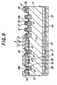
- Figs. 7-9 are cross sectional views showing successive manufacturing steps in a first embodiment of the static induction thyristor according to the present invention.
- the manufacturing step shown in Fig. 7 is similar to the conventional one shown in Fig. 3, in which P + -type regions 12 to constitute guard regions and field limiting rings and P + -type regions 13 to constitute gate regions are formed on an intrinsic (i) or an n-type silicon substrate 11, and thereafter, an n - -type silicon epitaxial growth layer 14 is formed. There-after, an n + -type diffusion layer 14' is formed by a well known diffusion method.
- concave portions 15A and 15B are formed at the positions corresponding to the guard regions and the field limiting rings by wet-etching so as to be extended to the silicon substrate 11 from the surface of the epitaxial growth layer 14.
- the narrow concave portions 15B are formed so as to correspond to the respective field limiting rings, so a conventional wide concave portion to cover some of plural field limiting rings is not formed.
- the concave portions 15B have the almost same width as that of the concave portions 15A corresponding to the guard regions.
- the concave portions 15A and 15B have the almost same lateral sectional shape, and the spread of the depletion layer is not likely to be disturbed, so that a desired forward voltage-resistance can be realized.
- the concave portions 15A enable cathode side unit segments S composed of channels 16 and n + -type cathode regions 17 to be formed between the adjacent concave portions 15A, and enable P + -type guard regions 18 to be formed under each of the concave portions 15A.
- the concave portions 15B enables p + -type field limiting rings 20 to be formed between the adjacent concave portions 15B.
- a silicon oxide film 21 is formed on the epitaxial growth layer 14 and the inner surfaces of the concave portions 15A and 15B, and is selectively removed to form openings, so that cathode electrodes 22 and gate electrodes 23 are formed.
- an n-type region 24, n + -type regions 25, p + -type regions 26 and an anode electrode 27 are formed on the back surface of the silicon substrate 11 on the back surface of the silicon substrate 11 on the back surface of the silicon substrate 11.
- Fig. 10 is an enlarged cross sectional view of the field limiting ring region.
- each field limiting ring 20 is defined by the concave portions 15B
- the n-type epitaxial growth layer 14 does not partially remain inside the concave portions because each concave portion 15B is narrower than the conventional one.
- the depletion layer which is generated at the off-state of the thyristor, is elongated beyond the field limiting rings 20 because the remaining parts of the epitaxial layer are separated from the silicon substrate 11, so that a sufficient large forward blocking voltage can be realized.
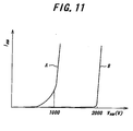
- the SIThy of the present invention shown in Fig. 10 can have the designed forward blocking voltage value as depicted by the curve B in Fig. 11.
- the conventional SIThy can have an only forward blocking voltage value of 1200V much smaller than the above designed value as depicted by the curve A in Fig. 11.
- a leak current does not occur nearly up to 2000V in the thyristor of the present invention although a leak current occurs over 500V in the conventional thyristor.
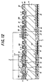
- Fig. 12 shows a second embodiment of the SIThy of the present invention.
- Reverse Conduction Static Induction Thyristor (RC-SIThy) having anti-parallel diodes is presented.
- R-SIThy Reverse Conduction Static Induction Thyristor
- plural p + -type isolation rings 41 are formed so as to surround the active regions including the channels 16, and a diode are formed at the outside of the isolation rings.
- the diode has plural p + -type embedded regions 42 which are formed with the p + -type gate regions 13 and embedded in the channel 16, plural p + -type surface regions 43 formed on the epitaxial growth layer 14 and an anode electrode 44 connected to the plural surface regions.
- the anode electrode 44 is connected to the cathode electrode 22.
- the plural p + -type field limiting rings 20 are formed at the outside of the anti-parallel diodes, and a channel limit ring 28 and an electrode 29 connected to the ring 28 are formed at the outside of the plural field limiting rings 20.
- the electrode 29 is held at a floating electric potential.
- the plural isolation rings 41 to constitute the isolation regions surrounding the active regions are defined by concave portions 15C having the same width and pitch as the ones of the concave portions 15A in the main device of the thyristor.
- Active etching species are supplied uniformly to the concave portions and etching-ended inactive etching species remain uniformly in the concave portions, so that all the concave portions are uniformly etched. Therefore, the epitaxial growth layer 14 does not almost remain in the concave portions between the adjacent isolation rings.
- the depletion layer is elongated under the field limiting rings 20 via the lower side of the isolation rings 41 when a given voltage is applied between the main electrodes at the off-state of the SIThy, and thus, a sufficient large forward blocking voltage can be realized as designed.
- the concave portions 15c to define the isolation rings 41 have the almost same lateral sectional shape as that of the concave portions 15C to define the guard regions 18 and the concave portions 15B to defined the field limiting rings 20.
- the field limiting rings and the isolation rings may be set to any number not less than two.
- the static induction device and the manufacturing method of the present invention can be applied for the above SIThy and RC-SIThy, but may be applied for a Static Induction Transistor (SIT).
- the etching process can be performed uniformly for the concave portions.
- the epitaxial growth layer does not partially remain in the concave portions and thus, the depletion layer can spread beyond the field limiting rings and the isolation rings, so that the forward blocking voltage can be sufficiently enhanced at off-state and the reliability of the static induction device can be developed.
- the concave portions to define the field limiting rings and the isolation rings have the almost same lateral sectional shape as that of the concave portions to define the channels, all the concave portions can have the planer uniform distribution and thus, the operation performance of the main device can be more improved.
Landscapes
- Junction Field-Effect Transistors (AREA)
- Thyristors (AREA)
Abstract
Description
Claims (12)
- A static induction semiconductor device comprising a one conduction-type semiconductor substrate, a one conduction-type epitaxial growth layer formed on one surface of the semiconductor substrate, plural concave portions which extend from a surface of the epitaxial growth layer to the substrate and define plural one main electrode regions composed of the epitaxial growth layer, plural opposite conduction-type gate regions embedded in the respective channel regions between the adjacent concave portions, plural opposite conduction-type guard regions, each being formed under each concave portion, the other main electrode regions formed on the other surface of the semiconductor substrate, and plural opposite conduction-type field limiting rings surrounding the one main electrode regions, the plural channel regions, the plural gate regions and the plural guard regions, each field limiting ring being formed under a part of the one conduction-type epitaxial growth layer sandwiched by the respective adjacent concave portions extending to the one surface of the semiconductor substrate from the epitaxial growth layer.
- A static induction semiconductor device as defined in claim 1, wherein the concave portions to define the field limiting rings and the concave portions to define the channel regions have the almost same lateral sectional size.
- A static induction semiconductor device as defined in claim 2, wherein the opposite conduction-type guard regions and the opposite conduction-type field limiting rings have the almost same junction depth deeper than that of the opposite conduction-type gate regions.
- A static induction semiconductor device as defined in any one of claims 1-3, wherein an electrode is provided on the epitaxial growth layer.
- A static induction semiconductor device as defined in any one of claims 1-3, wherein the epitaxial growth layer is covered with an insulating film.
- A reverse conduction static induction semiconductor device comprising a one conduction-type semiconductor substrate, a one conduction-type epitaxial growth layer formed on one surface of the semiconductor substrate, plural concave portions which extend from a surface of the epitaxial growth layer to the substrate and define plural one main electrode regions composed of the epitaxial growth layer, plural opposite conduction-type gate regions embedded in the respective channel regions between the adjacent concave portions, plural opposite conduction-type guard regions, each being formed under each concave portion, the other main electrode regions formed on the other surface of the semiconductor substrate, plural isolation rings surrounding the one main electrode regions, the plural channel regions, the plural gate regions and the plural guard regions, each isolation ring being composed of an opposite conduction-type region between respective adjacent concave portions extending to the one surface of the semiconductor substrate from the surface of the epitaxial growth layer under the epitaxial growth layer, an anti-parallel diode having an emitter region composed of an opposite conduction-type surface region formed at the one conduction-type semiconductor substrate and at least the epitaxial growth layer, and plural field limiting rings formed at the outside of the anti-parallel diode, each field limiting ring being composed of an opposite conduction-type region between respective adjacent concave portions extending to the one surface of the semiconductor substrate from the surface of the epitaxial growth layer.
- A reverse conduction static induction semiconductor device as defined in claim 6, wherein the concave portions to define the isolation rings and to define the field limiting rings have the almost same lateral sectional shape as that of the concave portions to define the channel regions.
- A reverse conduction static induction semiconductor device as defined in claim 7, wherein the opposite conduction-type guard regions, the opposite conduction-type isolation rings and the opposite conduction-type field limiting rings have the almost same junction depth deeper than that of the opposite conduction-type gate regions.
- A method for manufacturing a static induction semiconductor device having a one conduction-type semiconductor substrate, a one conduction-type epitaxial growth layer formed on one surface of the semiconductor substrate, plural concave portions which extend from a surface of the epitaxial growth layer to the substrate and define plural one main electrode regions composed of the epitaxial growth layer, plural opposite conduction-type gate regions embedded in the respective channel regions between the adjacent concave portions, plural opposite conduction-type guard regions, each being formed under each concave portion, the other main electrode regions formed on the other surface of the semiconductor substrate, and plural opposite conduction-type field limiting rings surrounding the one main electrode regions, the plural channel regions, the plural gate regions and the plural guard regions, each field limiting ring being formed under a part of the one conduction-type epitaxial growth layer sandwiched by the respective adjacent concave portions extending to the one surface of the semiconductor substrate from the epitaxial growth layer, comprising the steps of:forming opposite conduction-type regions to constitute the guard regions and the field limiting rings selectively at the one surface of the one conduction-type semiconductor substrate,forming opposite conduction-type regions to constitute the gate regions selectively at the one surface of the one conduction-type semiconductor substrate,forming a one conduction-type epitaxial growth layer on the one surface of the semiconductor substrate,forming the concave portions to define the channel regions and the field limiting rings so as to be extended to the one surface of the semiconductor substrate from the epitaxial growth layer,forming electrodes for the guard regions at the bottoms of the concave portions to define the channel regions, andforming electrodes for the one main electrode regions formed above the channel regions and the other main electrode regions formed on the other surface of the semiconductor substrate.
- A method for manufacturing a static induction semiconductor device as defined in claim 9, wherein the concave portions to define the field limiting rings and the concave portions to define the channel regions are formed so as to have the almost same lateral sectional size.
- A method for manufacturing a reverse conduction static induction semiconductor device comprising a one conduction-type semiconductor substrate, a one conduction-type epitaxial growth layer formed on one surface of the semiconductor substrate, plural concave portions which extend from a surface of the epitaxial growth layer to the substrate and define plural one main electrode regions composed of the epitaxial growth layer, plural opposite conduction-type gate regions embedded in the respective channel regions between the adjacent concave portions, plural opposite conduction-type guard regions, each being formed under each concave portion, the other main electrode regions formed on the other surface of the semiconductor substrate, plural isolation rings surrounding the one main electrode regions, the plural channel regions, the plural gate regions and the plural guard regions, each isolation ring being composed of an opposite conduction-type region between respective adjacent concave portions extending to the one surface of the semiconductor substrate from the surface of the epitaxial growth layer under the epitaxial growth layer, an anti-parallel diode having an emitter region composed of an opposite conduction-type surface region formed at the one conduction-type semiconductor and at least the epitaxial growth layer, and plural field limiting rings formed at the outside of the anti-parallel diode, each field limiting ring being composed of an opposite conduction-type region between respective adjacent concave portions extending to the one surface of the semiconductor substrate from the surface of the epitaxial growth layer, comprising the steps of:forming opposite conduction-type regions to constitute the guard regions, the isolation rings and the field limiting rings selectively at the one surface of the one conduction-type semiconductor substrate,forming opposite conduction-type regions to constitute the gate regions and the emitter region of the anti-parallel diode selectively at the one surface of the one conduction-type semiconductor substrate,forming the one conduction-type epitaxial growth layer on the one surface of the semiconductor substrate,forming the concave portions to define the channel regions, the isolation rings and the field limiting rings so as to be extended to the one surface of the semiconductor substrate from the epitaxial growth layer,forming an opposite conduction-type surface region to constitute the emitter region of the anti-parallel diode in the epitaxial growth layer,forming electrodes for the guard regions at the bottoms of the concave portions to define the channel regions, andforming electrodes for opposite conduction-type surface regions to constitute the one main electrode regions formed above the channel regions, the other main electrode regions formed on the other surface of the semiconductor substrate and the emitter region of the anti-parallel diode.
- A method for manufacturing a reverse conduction static induction semiconductor device as defined in claim 11, wherein the concave portions to define the channel regions, the isolation rings and the field limiting rings are formed so as to have the almost same lateral sectional size.
Applications Claiming Priority (2)
| Application Number | Priority Date | Filing Date | Title |
|---|---|---|---|
| JP29503299 | 1999-10-18 | ||
| JP29503299A JP4458588B2 (en) | 1999-10-18 | 1999-10-18 | Static induction semiconductor device and method for manufacturing the same |
Publications (3)
| Publication Number | Publication Date |
|---|---|
| EP1094524A2 true EP1094524A2 (en) | 2001-04-25 |
| EP1094524A3 EP1094524A3 (en) | 2003-05-28 |
| EP1094524B1 EP1094524B1 (en) | 2007-12-26 |
Family
ID=17815448
Family Applications (1)
| Application Number | Title | Priority Date | Filing Date |
|---|---|---|---|
| EP00309145A Expired - Lifetime EP1094524B1 (en) | 1999-10-18 | 2000-10-17 | A static induction semiconductor device and a method for manufacturing the same |
Country Status (4)
| Country | Link |
|---|---|
| US (1) | US6558996B1 (en) |
| EP (1) | EP1094524B1 (en) |
| JP (1) | JP4458588B2 (en) |
| DE (1) | DE60037562T2 (en) |
Cited By (3)
| Publication number | Priority date | Publication date | Assignee | Title |
|---|---|---|---|---|
| WO2007011294A1 (en) * | 2005-07-20 | 2007-01-25 | Cree Sweden Ab | Semiconductor device and a method for production thereof |
| EP2629333A3 (en) * | 2012-02-16 | 2014-10-29 | NGK Insulators, Ltd. | Semiconductor device and method for producing the same |
| CN115528019A (en) * | 2021-06-24 | 2022-12-27 | 无锡华润上华科技有限公司 | ESD protection device, protection circuit and preparation method |
Families Citing this family (6)
| Publication number | Priority date | Publication date | Assignee | Title |
|---|---|---|---|---|
| JP5210484B2 (en) * | 2004-02-23 | 2013-06-12 | 日本碍子株式会社 | Semiconductor device |
| JP4981244B2 (en) * | 2004-03-22 | 2012-07-18 | 日本碍子株式会社 | Semiconductor device |
| JP2013149956A (en) | 2011-12-22 | 2013-08-01 | Ngk Insulators Ltd | Semiconductor device |
| JP6120550B2 (en) | 2011-12-22 | 2017-04-26 | 日本碍子株式会社 | Semiconductor device |
| JP2012109601A (en) * | 2012-02-01 | 2012-06-07 | Ngk Insulators Ltd | Semiconductor device |
| JP2016187006A (en) * | 2015-03-27 | 2016-10-27 | 日本碍子株式会社 | Semiconductor device |
Family Cites Families (7)
| Publication number | Priority date | Publication date | Assignee | Title |
|---|---|---|---|---|
| US5175598A (en) * | 1978-01-06 | 1992-12-29 | Zaidan Hojin Handotai Kenkyu Shinkokai | Semiconductor switching device |
| JPS6443863A (en) | 1987-08-12 | 1989-02-16 | Hitachi Ltd | Pcm signal recording device |
| JPH04206574A (en) * | 1990-11-30 | 1992-07-28 | Yazaki Corp | Buried gate type semiconductor element and manufacture thereof |
| JPH07302896A (en) * | 1994-04-28 | 1995-11-14 | Ngk Insulators Ltd | Semiconductor device and manufacturing method thereof |
| JP3171301B2 (en) * | 1994-12-28 | 2001-05-28 | 矢崎総業株式会社 | Embedded gate type semiconductor device |
| US5682044A (en) * | 1995-01-31 | 1997-10-28 | Takashige Tamamushi | Reverse conducting thyristor with a planar-gate, buried-gate, or recessed-gate structure |
| EP0862221A4 (en) * | 1996-09-17 | 1999-06-09 | Ngk Insulators Ltd | SEMICONDUCTOR DEVICE |
-
1999
- 1999-10-18 JP JP29503299A patent/JP4458588B2/en not_active Expired - Lifetime
-
2000
- 2000-10-17 EP EP00309145A patent/EP1094524B1/en not_active Expired - Lifetime
- 2000-10-17 DE DE60037562T patent/DE60037562T2/en not_active Expired - Lifetime
- 2000-10-18 US US09/691,016 patent/US6558996B1/en not_active Expired - Lifetime
Cited By (5)
| Publication number | Priority date | Publication date | Assignee | Title |
|---|---|---|---|---|
| WO2007011294A1 (en) * | 2005-07-20 | 2007-01-25 | Cree Sweden Ab | Semiconductor device and a method for production thereof |
| US7768092B2 (en) | 2005-07-20 | 2010-08-03 | Cree Sweden Ab | Semiconductor device comprising a junction having a plurality of rings |
| EP2629333A3 (en) * | 2012-02-16 | 2014-10-29 | NGK Insulators, Ltd. | Semiconductor device and method for producing the same |
| US9048281B2 (en) | 2012-02-16 | 2015-06-02 | Ngk Insulators, Ltd. | Semiconductor device and method for producing the same |
| CN115528019A (en) * | 2021-06-24 | 2022-12-27 | 无锡华润上华科技有限公司 | ESD protection device, protection circuit and preparation method |
Also Published As
| Publication number | Publication date |
|---|---|
| JP2001119014A (en) | 2001-04-27 |
| JP4458588B2 (en) | 2010-04-28 |
| EP1094524A3 (en) | 2003-05-28 |
| DE60037562D1 (en) | 2008-02-07 |
| US6558996B1 (en) | 2003-05-06 |
| DE60037562T2 (en) | 2009-01-08 |
| EP1094524B1 (en) | 2007-12-26 |
Similar Documents
| Publication | Publication Date | Title |
|---|---|---|
| JP3413250B2 (en) | Semiconductor device and manufacturing method thereof | |
| EP1255302B1 (en) | Method for fabricating forward and reverse blocking devices | |
| US6221688B1 (en) | Diode and method for manufacturing the same | |
| CN1126180C (en) | Latch-up free power mos-bipolar transistor | |
| US5904544A (en) | Method of making a stable high voltage semiconductor device structure | |
| US9941383B2 (en) | Fast switching IGBT with embedded emitter shorting contacts and method for making same | |
| GB2154794A (en) | Vertical mosfet | |
| US6229196B1 (en) | Semiconductor device and fabrication method thereof | |
| JP4006879B2 (en) | Schottky barrier diode and manufacturing method thereof | |
| US11239352B2 (en) | Self-aligned and robust IGBT devices | |
| EP1094524B1 (en) | A static induction semiconductor device and a method for manufacturing the same | |
| US4357178A (en) | Schottky barrier diode with controlled characteristics and fabrication method | |
| KR0163875B1 (en) | Semiconductor device and manufacturing method | |
| JP2002261281A (en) | Method of manufacturing insulated gate bipolar transistor | |
| EP0665597A1 (en) | IGBT and manufacturing process therefore | |
| EP0756760B1 (en) | Semiconductor device with guard ring and process for its production | |
| US6107127A (en) | Method of making shallow well MOSFET structure | |
| JPH10335630A (en) | Semiconductor device and manufacturing method thereof | |
| JPH01149464A (en) | Semiconductor device | |
| EP0845813A1 (en) | Insulated gate bipolar transistor | |
| US12593477B2 (en) | Semiconductor device with anode trench | |
| JP3017783B2 (en) | Conduction modulation type MOSFET | |
| KR100281556B1 (en) | Integrated logic fabrication method using heterojunction dipole transistor | |
| JPH07135315A (en) | Semiconductor device | |
| KR100218263B1 (en) | Semiconductor device and manufacturing method thereof |
Legal Events
| Date | Code | Title | Description |
|---|---|---|---|
| PUAI | Public reference made under article 153(3) epc to a published international application that has entered the european phase |
Free format text: ORIGINAL CODE: 0009012 |
|
| AK | Designated contracting states |
Kind code of ref document: A2 Designated state(s): AT BE CH CY DE DK ES FI FR GB GR IE IT LI LU MC NL PT SE |
|
| AX | Request for extension of the european patent |
Free format text: AL;LT;LV;MK;RO;SI |
|
| PUAL | Search report despatched |
Free format text: ORIGINAL CODE: 0009013 |
|
| AK | Designated contracting states |
Designated state(s): AT BE CH CY DE DK ES FI FR GB GR IE IT LI LU MC NL PT SE |
|
| AX | Request for extension of the european patent |
Extension state: AL LT LV MK RO SI |
|
| 17P | Request for examination filed |
Effective date: 20031121 |
|
| AKX | Designation fees paid |
Designated state(s): CH DE FR GB LI SE |
|
| 17Q | First examination report despatched |
Effective date: 20061011 |
|
| GRAP | Despatch of communication of intention to grant a patent |
Free format text: ORIGINAL CODE: EPIDOSNIGR1 |
|
| GRAS | Grant fee paid |
Free format text: ORIGINAL CODE: EPIDOSNIGR3 |
|
| GRAA | (expected) grant |
Free format text: ORIGINAL CODE: 0009210 |
|
| AK | Designated contracting states |
Kind code of ref document: B1 Designated state(s): CH DE FR GB LI SE |
|
| REG | Reference to a national code |
Ref country code: GB Ref legal event code: FG4D |
|
| REG | Reference to a national code |
Ref country code: CH Ref legal event code: EP |
|
| REF | Corresponds to: |
Ref document number: 60037562 Country of ref document: DE Date of ref document: 20080207 Kind code of ref document: P |
|
| REG | Reference to a national code |
Ref country code: SE Ref legal event code: TRGR |
|
| PLBE | No opposition filed within time limit |
Free format text: ORIGINAL CODE: 0009261 |
|
| STAA | Information on the status of an ep patent application or granted ep patent |
Free format text: STATUS: NO OPPOSITION FILED WITHIN TIME LIMIT |
|
| 26N | No opposition filed |
Effective date: 20080929 |
|
| REG | Reference to a national code |
Ref country code: FR Ref legal event code: PLFP Year of fee payment: 17 |
|
| REG | Reference to a national code |
Ref country code: FR Ref legal event code: PLFP Year of fee payment: 18 |
|
| REG | Reference to a national code |
Ref country code: FR Ref legal event code: PLFP Year of fee payment: 19 |
|
| PGFP | Annual fee paid to national office [announced via postgrant information from national office to epo] |
Ref country code: FR Payment date: 20180913 Year of fee payment: 19 |
|
| PGFP | Annual fee paid to national office [announced via postgrant information from national office to epo] |
Ref country code: DE Payment date: 20181002 Year of fee payment: 19 Ref country code: SE Payment date: 20181011 Year of fee payment: 19 |
|
| PGFP | Annual fee paid to national office [announced via postgrant information from national office to epo] |
Ref country code: CH Payment date: 20181015 Year of fee payment: 19 Ref country code: GB Payment date: 20181017 Year of fee payment: 19 |
|
| REG | Reference to a national code |
Ref country code: DE Ref legal event code: R119 Ref document number: 60037562 Country of ref document: DE |
|
| REG | Reference to a national code |
Ref country code: CH Ref legal event code: PL |
|
| PG25 | Lapsed in a contracting state [announced via postgrant information from national office to epo] |
Ref country code: CH Free format text: LAPSE BECAUSE OF NON-PAYMENT OF DUE FEES Effective date: 20191031 Ref country code: LI Free format text: LAPSE BECAUSE OF NON-PAYMENT OF DUE FEES Effective date: 20191031 Ref country code: DE Free format text: LAPSE BECAUSE OF NON-PAYMENT OF DUE FEES Effective date: 20200501 |
|
| PG25 | Lapsed in a contracting state [announced via postgrant information from national office to epo] |
Ref country code: SE Free format text: LAPSE BECAUSE OF NON-PAYMENT OF DUE FEES Effective date: 20191018 |
|
| GBPC | Gb: european patent ceased through non-payment of renewal fee |
Effective date: 20191017 |
|
| PG25 | Lapsed in a contracting state [announced via postgrant information from national office to epo] |
Ref country code: FR Free format text: LAPSE BECAUSE OF NON-PAYMENT OF DUE FEES Effective date: 20191031 Ref country code: GB Free format text: LAPSE BECAUSE OF NON-PAYMENT OF DUE FEES Effective date: 20191017 |