EP1094488A2 - Protection circuit for traveling wave tubes having multiple input tones - Google Patents
Protection circuit for traveling wave tubes having multiple input tones Download PDFInfo
- Publication number
- EP1094488A2 EP1094488A2 EP00122727A EP00122727A EP1094488A2 EP 1094488 A2 EP1094488 A2 EP 1094488A2 EP 00122727 A EP00122727 A EP 00122727A EP 00122727 A EP00122727 A EP 00122727A EP 1094488 A2 EP1094488 A2 EP 1094488A2
- Authority
- EP
- European Patent Office
- Prior art keywords
- sensor
- circuit
- time constant
- twt
- stage
- Prior art date
- Legal status (The legal status is an assumption and is not a legal conclusion. Google has not performed a legal analysis and makes no representation as to the accuracy of the status listed.)
- Withdrawn
Links
Images

Classifications
-
- H—ELECTRICITY
- H01—ELECTRIC ELEMENTS
- H01J—ELECTRIC DISCHARGE TUBES OR DISCHARGE LAMPS
- H01J23/00—Details of transit-time tubes of the types covered by group H01J25/00
- H01J23/34—Circuit arrangements not adapted to a particular application of the tube and not otherwise provided for
-
- H—ELECTRICITY
- H01—ELECTRIC ELEMENTS
- H01J—ELECTRIC DISCHARGE TUBES OR DISCHARGE LAMPS
- H01J2225/00—Transit-time tubes, e.g. Klystrons, travelling-wave tubes, magnetrons
- H01J2225/34—Travelling-wave tubes; Tubes in which a travelling wave is simulated at spaced gaps
- H01J2225/36—Tubes in which an electron stream interacts with a wave travelling along a delay line or equivalent sequence of impedance elements, and without magnet system producing an H-field crossing the E-field
- H01J2225/38—Tubes in which an electron stream interacts with a wave travelling along a delay line or equivalent sequence of impedance elements, and without magnet system producing an H-field crossing the E-field the forward travelling wave being utilised
Definitions
- the present invention relates to a protection circuit for a traveling wave tube (TWT), and more particularly to a protection circuit for a traveling wave tube driven by multiple input tones.
- TWT traveling wave tube
- TWT 100 An exemplary traveling wave tube (TWT) 100 is shown in Figure 1.
- the elements of the TWT 100 are generally coaxially-arranged on along a TWT axis 102.
- the elements include an electron gun 104, a slow wave structure 106, a beam focusing arrangement 108 which surrounds the slow wave structure 106, a microwave signal input port 110 and a microwave signal output port 112 which are coupled to opposite ends of the slow wave structure 106, and a collector 114.
- a housing 116 is typically provided to protect the TWT elements.
- the electron gun 104 injects a beam of electrons into the slow wave structure 106.
- the electron beam has a given power level.
- the beam focusing arrangement 108 guides the electron beam through the slow wave structure 106.
- a microwave input signal 118 is inserted at the input port 110 and moves along the slow wave structure 106 to the output port 112.
- the slow wave structure 106 causes the phase velocity (i.e., the axial velocity of the phase front of the signal) of the microwave signal to approximate the velocity of the electron beam.
- the electrons of the beam are velocity modulated into bunches which interact with the slower microwave signal.
- kinetic energy is transferred from the electrons to the microwave signal causing the microwave signal to be amplified.
- the amplified signal is coupled from the output port 112 as a microwave output signal 120. After their passage through the slow wave detector 106, the electrons are collected in the collector.
- an individual power supply (not shown) is associated with each TWT and the power supply delivers the necessary bias voltages and currents.
- Standard protection circuits for TWT's are included in an external power conditioning unit (EPC).
- the protection circuit detects excessive helix current and either rapidly turns off the voltages to the TWT, or shuts down the inverters in a switching power supply to remove the voltages from the TWT.
- the standard protection circuit is typically a simple voltage-level detector with a short time-constant integrator for monitoring the helix current across a sense state resistor with an integrating operational amplifier, a Schmidt trigger circuit, or both. The detector is designed to detect an arc, fault, or overdrive situation and limit the total energy (in joules) that can be delivered to the TWT in order to avoid damage to the internal electrodes.
- Standard protection circuits are typically designed for a TWT driven by a single tone. However, in modern communication systems, it is more common to drive the TWT with multiple tones to increase utilization of the available bandwidth.
- Prior art protection circuits that use a second sensor, called line sensors, use the second sensor to measure input power to the power supply. The line sensor provides a very slow response and are only occasionally used.
- the sensitivity of the detector circuit In order to use a standard protection circuit for a multiple-tone driven application, the sensitivity of the detector circuit must be reduced by raising the peak threshold level, increasing the time constant, or both. The de-sensitization avoids spurious shut down from the protection circuit mistaking multi-tone phase-up with fault situations. However, desensitizing the circuit can lead to excessive energy being delivered to the tube in the event of a fault and excessive average power in the TWT when it is operated with only a single tone.
- the present invention is a protection circuit that protects a traveling wave tube from excessive helix current when the TWT is driven with multiple tones.
- the present invention independently detects the peak and average power levels associated with helix current interception in the TWT by a two-stage sense circuit. This allows the protection circuit to turn off the TWT in the appropriate situations, even in the presence of multiple tones and large helix current spikes.
- the protection circuit of the present invention has two detectors.
- a first detector is designed for the signature of arcs or high voltage faults which have fast rise times and high peak values of the helix current.
- the second detector is designed to limit the average power loading on the electrodes associated with the normal operation of a TWT. Average power loading has long time constants and lower helix currents.
- the dual sensor circuit eliminates spurious shutdowns and circuit damage that is caused by desensitized single stage detector. Safe operation with a plurality of tones and continuous-random-variation of the phase signals can be accomplished with the protection circuit of the present invention.
- Traveling Wave Tubes require several different voltages to be applied to its internal electrodes in order to amplify microwave signals and operate efficiently.
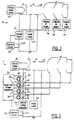
- Figures 2 and 3 are examples of typical power supply configurations, 10 and 11 respectively.
- Figures 2 and 3 show a cathode 12 of a TWT, an anode 14, a body 16, and three depressed electron collectors 18. It should be noted that while three collectors are shown, the present invention is not limited to applications involving three collectors and it is possible to use any number of collectors.
- An anode supply 20 and a cathode heater supply 22 are also shown.
- a sense resistor 28 is placed near ground potential and a protection circuit 30 monitors the voltage across the resistor.
- Figure 2 is an example of a single cathode-voltage power supply 10.
- a single cathode supply 32 is used, and a plurality of separate power supplies 34 are floated at the cathode potential.
- the plurality of separate power supplies 34 provide voltages to the depressed electron-beam collectors 18.
- FIG. 3 is an example of a power supply circuit 11 for providing voltages to a TWT with three collector stages 18.
- a cathode supply transformer 36 has several secondary taps 38. Each secondary tap 38 has a rectifier component 40 and a capacitor component 42 associated therewith. This arrangement, in combination with a cathode voltage regulator 44 produce several DC voltages that are used to provide the bias for the three stage depressed electron collectors 18.
- the protection circuit 30 used in the prior art is typically an operational amplifier (not shown) that monitors the voltage across the sense resistor 28.
- the voltage across the sense resistor 28 is proportional to the amount of beam current that hits the body 16 in the TWT.
- the protection circuit 30 in the prior art usually includes an integrator circuit (not shown) to filter out high frequency noise and permit some short duration transient excursions to occur without shutting down the power supply.
- the sensitivity of prior art protection circuits determined by the time constant of the integrator and the reference level of the operational amplifier, determines the amount of energy that is allowed to be deposited in the TWT in the event of a fault. Depending on the size and power handling characteristics of the TWT, energy levels of 0.1 to 10 joules are allowed.
- the varying phase causes a time-dependent change in the instantaneous electric field in the TWT, which modifies the helix current sensed by the protection circuit 30.
- the signal measured across the sense resistor 28 will contain large, varying current spikes of short duration. While the average power level of the TWT output and the average power dissipation in the TWT may not change significantly, the large helix current oscillations associated with multiple tones appears as a fault condition to the protection circuit 30.
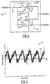
- a schematic representation of the protection circuit 30 of the present invention is shown in Figure 4.
- a dual sensor arrangement of two operational amplifiers monitoring the voltage across the sense resistor (not shown in Figure 3) is provided.
- a first sensor 52 is designed to have a time constant and peak current that is different from the time constant and peak current for a second sensor 54.
- the two sensors 52 and 54 are tied together by a logic "OR" function so that the voltages on the TWT, either a high current or a long-time-scale power condition, can be removed before damage occurs.
- the first sensor 52 has a time constant and peak current level that will detect rapid fault situations and protect the TWT from arcing.
- the second sensor 54 has a longer time constant and a lower peak threshold level such that the long-time-scale power (or energy) deposited on the TWT components does not damage the TWT.
- the values set for the time constants and current thresholds are determined by the power and energy handling characteristics of the TWT.
- the first sensor 52 is called a fast response stage and, in the present example, the operational amplifier 56 circuit has a time constant of 1.3 msec. and a peak threshold value of 30 mA.
- the second detector 54 or slow response stage, has an operational amplifier 58 circuit having a time constant of 750 msec and a threshold value of 18 mA. A sudden increase in the helix current over 30 mA will be detected by the first detector 52 and will cause the power supply to be turned off if the spike in current lasts for longer than 1.3 msec.
- the second detector 54 will protect the TWT against average power overload should the helix current remain below 18 mA for longer than 750 msec.
- Both detector circuits 52 and 54 have capacitors 60 across feedback resistors 62 so that two different and independent time constants can be obtained.
- the error-induced loading on the sense resistor due to the presence of the sensors 52 and 54 consists of simply a large resistance and no capacitance.
- the two sensors are isolated from each other in a logic arrangement through diodes 64.
- the diodes 64 are placed within the feedback loops of the operational amplifiers 56 and 58 so that all of the diode forward drop is canceled out, which results in minimal error in sensing the voltage across the sense resistor.
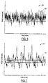
- FIG. 5 An example of the helix current measured across the sense resistor for a TWT producing an average of 126 Watts of power in two tones 70 is shown in Figure 5.
- the helix current oscillates due to the electric field of the two tones constructively and destructively interfering in the tube as a function of time associated with the different frequency and phase of the tones.
- the average helix current 72 in this example, is about 5 mA, and the peak current is about 10 mA.
- Figure 7 is an example of the voltage across the sense resistor when the phases of the different tones are randomly varied by a tone generator at a rate of eight times a second 90, (which is an industry standard for testing communication amplifiers).
- a tone generator at a rate of eight times a second 90, (which is an industry standard for testing communication amplifiers).
- the phase of the 8 tones is correct, the electric field of the signals in the TWT constructively interfere and result in a large instantaneous field in the TWT, which causes an increase in the helix current from the average level 92 of 9 mA to over 30 mA.
- phase stackup The continuous changing of the phase at 8 Hz means that the TWT must occasionally handle these high electric fields and helix currents associated with the constructive addition of multiple tones when the phase is correct, known as "phase stackup", for a duration of at least 125 msec. Since the undesirable phase condition statistically can occur immediately again, the TWT must actually handle several of these events for a time of nearly half a second.
- the prior art single op-amp sense circuit must be desensitized by increasing the integration time, the threshold reference level, or both so as to not trip on the high peak current spikes discussed with reference to Figure 7. Desensitizing the circuit prevents the TWT from being adequately protected for single or even two-tone operation because the trip levels are set to high to protect the tube.
- Implementing the dual sensor protection circuit 30 of the present invention eliminates both spurious shut downs and circuit damage that plagues a de-sensitized single-stage detector of the prior art.
- the dual sensor circuit 30 of the present invention allows safe operation without spurious shut-downs and has been accomplished with up to 16 tones with continuous-random-variation of the phase of the signals into the TWT.
Landscapes
- Amplifiers (AREA)
- Monitoring And Testing Of Nuclear Reactors (AREA)
- Investigating Or Analyzing Materials By The Use Of Magnetic Means (AREA)
Abstract
Description
Claims (8)
- A protection circuit (30) for a TWT (100) having multiple tone operation, said circuit (30) comprising:a first stage sensor (52) having a predetermined time constant and a predetermined current threshold;
characterized by:a second stage sensor (54) isolated from said first stage sensor (52) by a logic "OR" arrangement (64), said second stage sensor (54) having a predetermined time constant and a predetermined current threshold that is different from said predetermined time constant and said predetermined current threshold for said first stage sensor (52). - The circuit (30) of claim 1, characterized in that said first and second stage sensors (52, 54) are isolated from each other by diodes (64).
- The circuit (30) of claim 1 or 2, characterized in that said first stage sensor (52) has an operational amplifier circuit (56) designed such that said time constant is low and said threshold current is high relative to operating conditions for said TWT (100), and said second stage sensor (54) has an operational amplifier circuit (58) designed such that said time constant is higher than said time constant for said first stage sensor (52) and said threshold current is lower than said threshold current for said first stage sensor (52).
- The circuit of claim 3, characterized in that said operational amplifier circuits (56, 58) further comprise resistors (62) in a feedback loop, said resistors (62) having capacitors (60) connected across them for implementing separate and distinct time constants for said first and second stage sensors (52, 54).
- The circuit (30) of claim 4, characterized in that said feedback loops for said first and second stage sensors (52, 54) further comprise said diodes (64) for isolating said first and second stage sensors (52, 54).
- A dual sensor protection circuit (30) for a TWT (100) having multiple tone operation, said dual sensor protection circuit (30) comprising a first sensor (52),
characterized by:said first sensor (52) having a fast response; anda second sensor (54), logically "OR"ed with said first sensor (52), said second sensor (54) having a slow response. - The circuit of claim 6, characterized by:a first operational amplifier (56) having a feedback loop;a first resistor (62) in said feedback loop;a first capacitor (60) across said resistor for implementing a first time constant;a first diode (64) in said feedback loop;a second operational amplifier (58) having a feedback loop;a second resistor (62) in said feedback loop;a second capacitor (60) across said resistor (62) for implementing a second time constant, whereby said second time constant is longer than said first time constant;a second diode (64) in said feedback loop whereby said first and second diodes provide said logic "OR" connection between said first and second operational amplifiers (56, 58).
- A traveling wave tube mechanism (100) comprising:an electron gun (104) configured to generate an electron beam;a slow wave structure (106) positioned so that the electron beam passes through said slow wave structure (106);a beam focusing structure (108) arranged to confine the electron beam within the slow wave structure (106);a collector (114; 18) for collecting the electron beam;a power supply (10; 11) for applying voltages to said electron gun; anda protection circuit (30) for said TWT (100),
characterized in that said protection circuit (30) is a protection circuit (30) according to any of claims 1 to 7.
Applications Claiming Priority (2)
| Application Number | Priority Date | Filing Date | Title |
|---|---|---|---|
| US422876 | 1999-10-21 | ||
| US09/422,876 US6324041B1 (en) | 1999-10-21 | 1999-10-21 | Protection circuit for traveling wave tubes having multiple input tones |
Publications (2)
| Publication Number | Publication Date |
|---|---|
| EP1094488A2 true EP1094488A2 (en) | 2001-04-25 |
| EP1094488A3 EP1094488A3 (en) | 2004-02-11 |
Family
ID=23676786
Family Applications (1)
| Application Number | Title | Priority Date | Filing Date |
|---|---|---|---|
| EP00122727A Withdrawn EP1094488A3 (en) | 1999-10-21 | 2000-10-18 | Protection circuit for traveling wave tubes having multiple input tones |
Country Status (2)
| Country | Link |
|---|---|
| US (1) | US6324041B1 (en) |
| EP (1) | EP1094488A3 (en) |
Families Citing this family (4)
| Publication number | Priority date | Publication date | Assignee | Title |
|---|---|---|---|---|
| US6586883B1 (en) * | 2001-12-20 | 2003-07-01 | Lockheed Martin Corporation | Method and apparatus for detecting individual TWT helix current for multiple TWT loads |
| CN100416965C (en) * | 2004-10-12 | 2008-09-03 | 昆明理工大学 | Detection method for fault near voltage zero crossing in traveling wave protection |
| CN102081155B (en) * | 2009-11-30 | 2013-02-20 | 上海卫星工程研究所 | Safe use method of satellite-loaded travelling wave tube |
| KR102954550B1 (en) * | 2024-07-01 | 2026-04-21 | 엘아이지디펜스앤에어로스페이스 주식회사 | Circuit and control method for heater current limiting therefor by heating mode of traveling-wave tube amplifier |
Family Cites Families (6)
| Publication number | Priority date | Publication date | Assignee | Title |
|---|---|---|---|---|
| US3890545A (en) * | 1974-04-12 | 1975-06-17 | Us Navy | Traveling-wave-tube protection circuit |
| JPS55113239A (en) * | 1979-02-23 | 1980-09-01 | Nec Corp | Power source device for traveling-wave tube |
| DE3610524C2 (en) * | 1986-03-27 | 1995-06-22 | Thomson Tubes Electroniques | Circuit arrangement for protection against thermal overload of traveling wave tube amplifiers with multi-collector traveling wave tubes |
| JPH0391816A (en) * | 1989-09-05 | 1991-04-17 | Nec Corp | Protection circuit |
| US5932971A (en) | 1997-06-05 | 1999-08-03 | Hughes Electronics Corp | Optimally designed traveling wave tube for operation backed off from saturation |
| US5942852A (en) | 1997-06-05 | 1999-08-24 | Hughes Electronics Corporation | Efficient, highly linear traveling wave tube using collector with high backstreaming current under saturated drive |
-
1999
- 1999-10-21 US US09/422,876 patent/US6324041B1/en not_active Expired - Fee Related
-
2000
- 2000-10-18 EP EP00122727A patent/EP1094488A3/en not_active Withdrawn
Also Published As
| Publication number | Publication date |
|---|---|
| US6324041B1 (en) | 2001-11-27 |
| EP1094488A3 (en) | 2004-02-11 |
Similar Documents
| Publication | Publication Date | Title |
|---|---|---|
| CA2960139C (en) | Arc fault circuit interrupter detector systems including super regenerative high frequency receiver | |
| EP3907753A1 (en) | Rf power generator with analogue and digital detectors and method of operating such a power geberator | |
| CN101478139A (en) | Multi-path large power velocity modulated valve overcurrent real-time protection apparatus having on-line self-detection function | |
| US3694659A (en) | Automatic control circuit for image intensifier | |
| US6324041B1 (en) | Protection circuit for traveling wave tubes having multiple input tones | |
| US6262536B1 (en) | Crowbar circuit for linear beam device having multi-stage depressed collector | |
| US4860146A (en) | Differential current protection circuit breaker | |
| JPH0398298A (en) | X-ray apparatus | |
| JPH1198835A (en) | H-bridge booster circuit | |
| US7071624B2 (en) | Microwave tube system and microwave tube | |
| US3890545A (en) | Traveling-wave-tube protection circuit | |
| US4745369A (en) | Circuit arrangement for protection against thermal overload of traveling wave tube amplifiers having multicollector traveling wave tubes | |
| US6586883B1 (en) | Method and apparatus for detecting individual TWT helix current for multiple TWT loads | |
| US5374827A (en) | Bias for a conversion dynode in an electron multiplier | |
| KR102376455B1 (en) | Apparatus and method for laser energy measurement in laser amplifier system of high energy | |
| JP2002176034A (en) | Abnormal discharge automatic prevention device in plasma etching | |
| CN119182284A (en) | Ripple signal processing circuit, high-voltage power supply circuit and high-voltage power supply device | |
| US7310214B2 (en) | Inductive output tube (IOT) control circuit | |
| US8427058B2 (en) | Traveling-wave tube turn-off body energy circuit | |
| JPH0961537A (en) | Photodetector | |
| JPH0143481B2 (en) | ||
| KR102752880B1 (en) | High-voltage generator with status monitoring and flexible output control | |
| JPH08254552A (en) | Current sensor | |
| JP2000311649A (en) | Ion detector | |
| KR20250070370A (en) | Apparatus for detecting arc and operating method thereof |
Legal Events
| Date | Code | Title | Description |
|---|---|---|---|
| PUAI | Public reference made under article 153(3) epc to a published international application that has entered the european phase |
Free format text: ORIGINAL CODE: 0009012 |
|
| AK | Designated contracting states |
Kind code of ref document: A2 Designated state(s): AT BE CH CY DE DK ES FI FR GB GR IE IT LI LU MC NL PT SE |
|
| AX | Request for extension of the european patent |
Free format text: AL;LT;LV;MK;RO;SI |
|
| PUAL | Search report despatched |
Free format text: ORIGINAL CODE: 0009013 |
|
| AK | Designated contracting states |
Kind code of ref document: A3 Designated state(s): AT BE CH CY DE DK ES FI FR GB GR IE IT LI LU MC NL PT SE |
|
| AX | Request for extension of the european patent |
Extension state: AL LT LV MK RO SI |
|
| 17P | Request for examination filed |
Effective date: 20040806 |
|
| AKX | Designation fees paid |
Designated state(s): DE FR |
|
| 17Q | First examination report despatched |
Effective date: 20050203 |
|
| RAP1 | Party data changed (applicant data changed or rights of an application transferred) |
Owner name: THE BOEING COMPANY |
|
| RAP1 | Party data changed (applicant data changed or rights of an application transferred) |
Owner name: L-3 COMMUNICATIONS - ELECTRON TECHNOLOGIES, INC. |
|
| STAA | Information on the status of an ep patent application or granted ep patent |
Free format text: STATUS: THE APPLICATION IS DEEMED TO BE WITHDRAWN |
|
| 18D | Application deemed to be withdrawn |
Effective date: 20060503 |