EP1094350A2 - Optical projection lens system - Google Patents
Optical projection lens system Download PDFInfo
- Publication number
- EP1094350A2 EP1094350A2 EP00119874A EP00119874A EP1094350A2 EP 1094350 A2 EP1094350 A2 EP 1094350A2 EP 00119874 A EP00119874 A EP 00119874A EP 00119874 A EP00119874 A EP 00119874A EP 1094350 A2 EP1094350 A2 EP 1094350A2
- Authority
- EP
- European Patent Office
- Prior art keywords
- lens system
- optical projection
- projection lens
- lens
- waist
- Prior art date
- Legal status (The legal status is an assumption and is not a legal conclusion. Google has not performed a legal analysis and makes no representation as to the accuracy of the status listed.)
- Ceased
Links
- 230000003287 optical effect Effects 0.000 title claims abstract description 32
- 230000005855 radiation Effects 0.000 claims abstract description 10
- 230000001902 propagating effect Effects 0.000 claims abstract description 9
- WUKWITHWXAAZEY-UHFFFAOYSA-L calcium difluoride Chemical compound [F-].[F-].[Ca+2] WUKWITHWXAAZEY-UHFFFAOYSA-L 0.000 claims description 9
- 229910001634 calcium fluoride Inorganic materials 0.000 claims description 9
- 239000000463 material Substances 0.000 claims description 9
- 238000012937 correction Methods 0.000 claims description 6
- 238000001393 microlithography Methods 0.000 claims description 4
- VYPSYNLAJGMNEJ-UHFFFAOYSA-N Silicium dioxide Chemical compound O=[Si]=O VYPSYNLAJGMNEJ-UHFFFAOYSA-N 0.000 claims description 3
- 238000000034 method Methods 0.000 claims description 3
- 230000008569 process Effects 0.000 claims description 3
- 210000001015 abdomen Anatomy 0.000 claims description 2
- KRHYYFGTRYWZRS-UHFFFAOYSA-M Fluoride anion Chemical compound [F-] KRHYYFGTRYWZRS-UHFFFAOYSA-M 0.000 claims 1
- 230000005499 meniscus Effects 0.000 claims 1
- 210000001624 hip Anatomy 0.000 description 7
- 230000004075 alteration Effects 0.000 description 4
- 238000000206 photolithography Methods 0.000 description 4
- 239000004065 semiconductor Substances 0.000 description 3
- 238000007792 addition Methods 0.000 description 2
- 230000000694 effects Effects 0.000 description 2
- 238000004519 manufacturing process Methods 0.000 description 2
- 238000012986 modification Methods 0.000 description 2
- 230000004048 modification Effects 0.000 description 2
- 238000006467 substitution reaction Methods 0.000 description 2
- 230000008901 benefit Effects 0.000 description 1
- 238000005056 compaction Methods 0.000 description 1
- 238000010276 construction Methods 0.000 description 1
- 238000013461 design Methods 0.000 description 1
- 230000009467 reduction Effects 0.000 description 1
Images

Classifications
-
- G—PHYSICS
- G03—PHOTOGRAPHY; CINEMATOGRAPHY; ANALOGOUS TECHNIQUES USING WAVES OTHER THAN OPTICAL WAVES; ELECTROGRAPHY; HOLOGRAPHY
- G03F—PHOTOMECHANICAL PRODUCTION OF TEXTURED OR PATTERNED SURFACES, e.g. FOR PRINTING, FOR PROCESSING OF SEMICONDUCTOR DEVICES; MATERIALS THEREFOR; ORIGINALS THEREFOR; APPARATUS SPECIALLY ADAPTED THEREFOR
- G03F7/00—Photomechanical, e.g. photolithographic, production of textured or patterned surfaces, e.g. printing surfaces; Materials therefor, e.g. comprising photoresists; Apparatus specially adapted therefor
- G03F7/20—Exposure; Apparatus therefor
-
- G—PHYSICS
- G02—OPTICS
- G02B—OPTICAL ELEMENTS, SYSTEMS OR APPARATUS
- G02B13/00—Optical objectives specially designed for the purposes specified below
- G02B13/14—Optical objectives specially designed for the purposes specified below for use with infrared or ultraviolet radiation
- G02B13/143—Optical objectives specially designed for the purposes specified below for use with infrared or ultraviolet radiation for use with ultraviolet radiation
-
- G—PHYSICS
- G02—OPTICS
- G02B—OPTICAL ELEMENTS, SYSTEMS OR APPARATUS
- G02B13/00—Optical objectives specially designed for the purposes specified below
- G02B13/24—Optical objectives specially designed for the purposes specified below for reproducing or copying at short object distances
-
- G—PHYSICS
- G03—PHOTOGRAPHY; CINEMATOGRAPHY; ANALOGOUS TECHNIQUES USING WAVES OTHER THAN OPTICAL WAVES; ELECTROGRAPHY; HOLOGRAPHY
- G03F—PHOTOMECHANICAL PRODUCTION OF TEXTURED OR PATTERNED SURFACES, e.g. FOR PRINTING, FOR PROCESSING OF SEMICONDUCTOR DEVICES; MATERIALS THEREFOR; ORIGINALS THEREFOR; APPARATUS SPECIALLY ADAPTED THEREFOR
- G03F7/00—Photomechanical, e.g. photolithographic, production of textured or patterned surfaces, e.g. printing surfaces; Materials therefor, e.g. comprising photoresists; Apparatus specially adapted therefor
- G03F7/70—Microphotolithographic exposure; Apparatus therefor
- G03F7/70216—Mask projection systems
- G03F7/70241—Optical aspects of refractive lens systems, i.e. comprising only refractive elements
Definitions
- This invention generally relates to an optical projection system comprising a light source, a mask holder, a projection lens system, and specifically relates to an optical projection system for photolithography used in producing micro structured devices such as integrated circuits or other semiconductor devices.
- photolithography transfers an image from an photographic mask to a resultant pattern on a semiconductor wafer.
- Such photolithography generally includes a light exposure process, in which a semiconductor wafer is exposed to light having information of a mask pattern.
- Optical projection systems are used to perform the light exposure process.
- the transferred mask patterns are very fine, so that optical projection lens systems are required to have a high resolution.
- the high resolution necessitates a large numerical aperture of the optical projection lens system and also a nearly no aberration of the optical projection lens system in the light exposure field.
- the shown projection lens system comprises 6 lens groups.
- the first, third, fifth and the sixth lens groups have positive refractive power and the second and fourth lens groups have negative refractive power.
- aspherical surfaces are in the fourth and fifth lens groups.
- the optical projection lens system of the invention comprises in a direction of the light a first lens group having positive refractive power and a second lens group having negative refractive power and establishing a beam waist of minimal beam height.
- a further lens arrangement follows the second lens group.
- At least one lens, which is arranged before first beam waist, has an aspherical surface. Further lenses comprising aspherical surfaces in all other groups will be helpful to reduce the needed amount of material and to reduce the length of the optical projection lens system.
- the optical projection lens system shown in figure 1 comprises 30 lenses 1 - 30.
- This shown projection lens system is for wafer manufacture.
- a light source with a narrow bandwidth is used for illuminating a mask 103, which is positioned at 0, a light source with a narrow bandwidth is used.
- an excimer laser which is not shown in the drawing, is used.
- the shown projection lens system is capable to be operated at 193,3 nm with a high numerical aperture of 0.7.
- a projection system comprising with this projection lens system the scale of the mask 103 projected on a wafer is reduced, wherein the wafer is positioned on 0'.
- the factor of scale reduction is 4 and the distance of 0 to 0' is 1000 mm.
- the illuminated image field is rectangular, e.g. 7 x 20 to 15 x 30 mm 2 .
- this projection lens system comprises a first lens group G1 comprising lenses 1 to 7 and a second lens group G2 comprising lenses 8 to 14, and a further lens arrangement G3 comprising lenses 15 to 30.
- the first lens group G1 has positive refractive power and ends with a lens 7 of positive refractive power.
- the first lens 8 of the second lens group G2 is the first lens 8 behind the first belly of the projection lens system 100, which has a concave shaped lens surface 31 on the image side.
- this concave surface 31 has an aspherical shape. This aspherical surface 31 helps to reduce the track length, the number of needed lenses and to get a high image quality over the whole illuminated image field.
- This second lens group G2 has negative refractive power and comprises a clearly defined waist 37 , which comprises seven lenses. The high number of lenses are needed for petzval correction, because there is only one clearly defined waist. There are three negative lenses 8-10 arranged in front of a lens 11 of positive refractive power in the middle of the lens group G2. Behind this positive lens 11 there are further three negative lenses 12-15.
- the first lens 15 of the following lens arrangement G3 has positive refractive power. This is the first lens 15 of positive refractive power behind the lens 11 in the middle of the lens group G2.
- This lens arrangement G 3 has positive refractive power and comprises lenses 15-30 of different materials and a aperture stop 41.
- CaF 2 lenses 16, 17, 19, 21, 22, 29 and 30 are used.
- the other lenses are of quartz glass.
- These CaF 2 lenses are especially used for correction of chromatic aberration.
- This system comprises doublets D1, D2 and D3, which comprise a CaF 2 lens with positive refractive power followed by a quartz glass lens of negative refractive power. If no correction of chromatic aberration is required, as usual in 248 nm systems, or possible with very narrow laser bandwidth, there can be taken single lenses instead of the doublets D1 - D3 with the advantage of reducing the needed material and lenses.
- a very shallow waist 37 is recognizable between lens 20 and lens 21.
- the lens arrangement G3 has an maximal diameter of 238 mm.
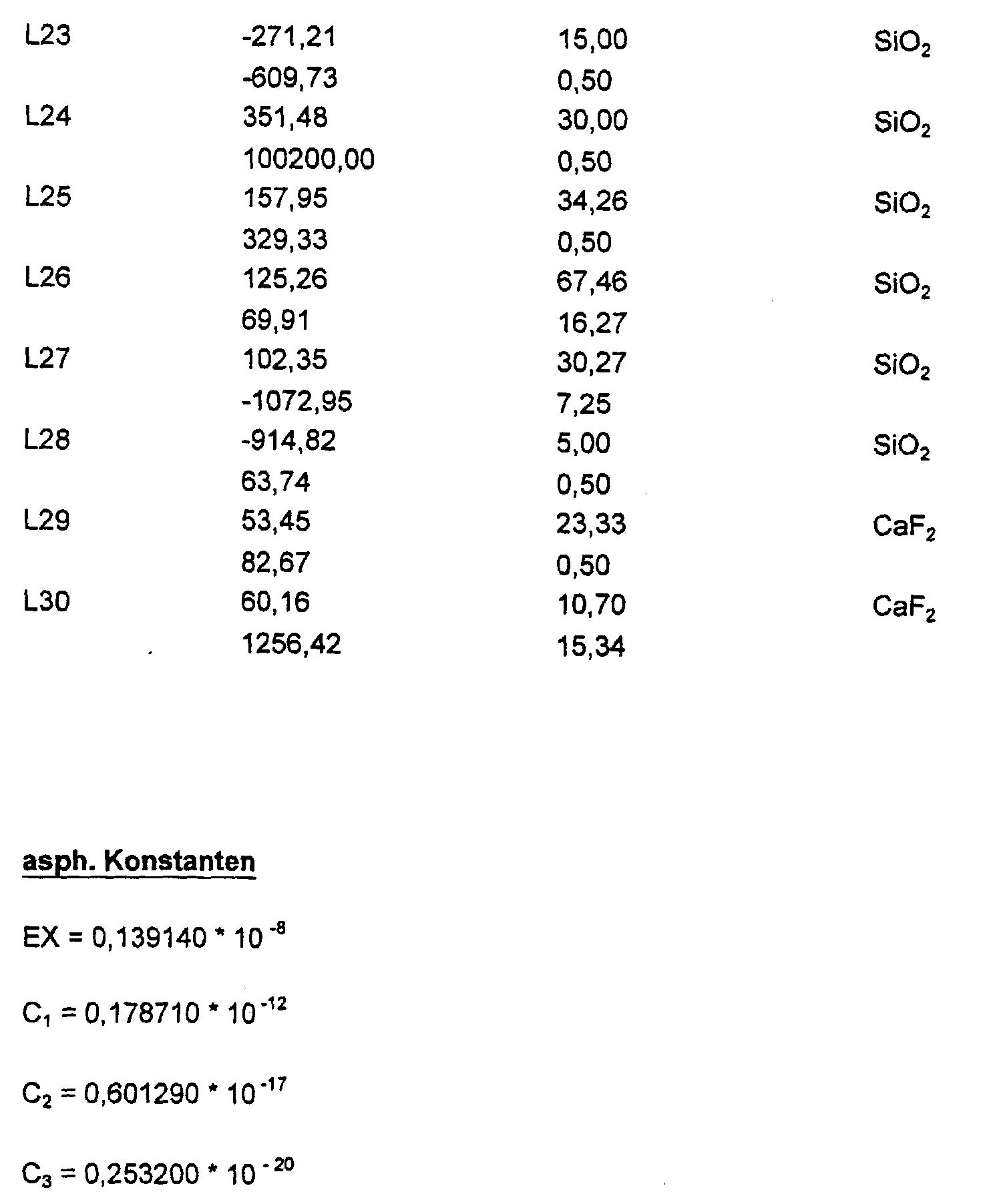
- the lens data of this embodiment are listed in table 1.
Landscapes
- Physics & Mathematics (AREA)
- General Physics & Mathematics (AREA)
- Optics & Photonics (AREA)
- Health & Medical Sciences (AREA)
- Toxicology (AREA)
- Lenses (AREA)
- Exposure And Positioning Against Photoresist Photosensitive Materials (AREA)
- Exposure Of Semiconductors, Excluding Electron Or Ion Beam Exposure (AREA)
Abstract
- a first lens group having positive refractive power
- a second lens group having negative refractive power and comprises a waist with a minimum diameter of the propagating radiation
- a further lens arrangement with positive refracting power, which follows the
second lens group,
wherein at least one lens of the projection lens system, which is arranged in front of the waist comprises an aspherical surface.
Description
- Figure 1
- is a cross section of an optical projection lens system according to an embodiment of the invention with only one clearly defined waist;

Claims (17)
- An optical projection lens system for microlithography comprising in direction of propagating radiationa first lens group having positive refractive power,a second lens group having negative refractive power and comprising a waist with a minimum diameter of the propagating radiation,a further lens arrangement with positive refracting power, which follows the second lens group,
wherein lenses, which comprises an aspherical surface, are arranged in front of the waist. - An optical projection lens system for microlithography comprising in direction of propagating radiationa first lens group having positive refractive power,a second lens group having negative refractive power and comprising a waist with a minimum diameter of propagating radiation,a further lens arrangement with positive refracting power, which follows the second lens group,
wherein the projection lens system comprises only one clearly defined waist and
wherein at least one lens comprises an aspherical surface. - An optical projection lens system for microlithography comprising in direction of propagating radiationa first lens group having positive refractive power,a second lens group having negative refractive power and comprising a waist with a minimum diameter of the propagating radiation,a further lens arrangement with positive refracting power, which follows the second lens group,
wherein the projection lens system comprises only one clearly defined waist,
wherein the numerical aperture is greater than 0.65. - An optical projection lens system of claim 1 or 2 or 3, wherein only the second lens group comprises an aspherical surface.
- An optical projection lens system of claim 1 or 2 or 3, wherein the lens arrangement comprises a second shallow waist.
- An optical projection lens system of claim 1 or 2 or 3, wherein the lens comprising the aspherical surface is an meniscus shaped lens.
- An optical projection lens system of at least one of the claims 1 to 6, wherein at least a second material is used for chromatic correction.
- An optical projection lens system of at least one of the claims 1 to 7, wherein the first material is quartz glass and wherein the second material is a fluoride.
- An optical projection lens system of claims 1 to 8, wherein the second material is used in the positive lens elements nearby the aperture stop.
- An optical projection lens system of claims 1 to 9, wherein CaF2 is the second material used for 193 nm.
- An optical projection lens system of claim 1 or 2 or 3 , wherein at least two of the lenses of the lens arrangement in front of the aperture stop are of CaF2.
- An optical projection lens system of at least one of claims 1 to 11, wherein the numerical aperture on the image side of the projection lens system is greater than 0.65, preferable 0,7 and more.
- An optical projection lens system of at least one of the claims 1 to 12, wherein at least three CaF2 lenses are bi-convex lenses.
- An optical projection lens system of at least one of the claims 1 to 13, wherein the last lens element is a CaF2 lens.
- An optical projection lens system of at least one of the claims 1 to 14, wherein an excimer laser is used as a light source emitting radiation of 250 nm and shorter wavelength.
- An optical projection lens system of at least one of the claims 1 to 15, wherein the optical projection lens system comprises only two bellies.
- Process for producing microstructured devices, wherein a wafer with a light sensitive layer is exposed by UV- light using an optical projection lens system of one of the claims 1 to 14 and using a mask for defining the structure of the device, wherein the light sensitive layer is developed to get the microstructured device.
Applications Claiming Priority (2)
| Application Number | Priority Date | Filing Date | Title |
|---|---|---|---|
| US16079999P | 1999-10-21 | 1999-10-21 | |
| US160799P | 1999-10-21 |
Publications (2)
| Publication Number | Publication Date |
|---|---|
| EP1094350A2 true EP1094350A2 (en) | 2001-04-25 |
| EP1094350A3 EP1094350A3 (en) | 2001-08-16 |
Family
ID=22578507
Family Applications (1)
| Application Number | Title | Priority Date | Filing Date |
|---|---|---|---|
| EP00119874A Ceased EP1094350A3 (en) | 1999-10-21 | 2000-09-13 | Optical projection lens system |
Country Status (5)
| Country | Link |
|---|---|
| US (4) | US6560031B1 (en) |
| EP (1) | EP1094350A3 (en) |
| JP (1) | JP2001141995A (en) |
| KR (1) | KR100832153B1 (en) |
| TW (1) | TW451076B (en) |
Cited By (10)
| Publication number | Priority date | Publication date | Assignee | Title |
|---|---|---|---|---|
| WO2002052303A3 (en) * | 2000-12-22 | 2002-10-31 | Zeiss Carl Semiconductor Mfg | Projection lens |
| US6538821B2 (en) | 1997-09-22 | 2003-03-25 | Nikon Corporation | Projection optical system |
| US6556353B2 (en) | 2001-02-23 | 2003-04-29 | Nikon Corporation | Projection optical system, projection exposure apparatus, and projection exposure method |
| US6606144B1 (en) | 1999-09-29 | 2003-08-12 | Nikon Corporation | Projection exposure methods and apparatus, and projection optical systems |
| WO2003077037A1 (en) * | 2002-03-08 | 2003-09-18 | Carl Zeiss Smt Ag | Refractive projection objective for immersion lithography |
| US6674513B2 (en) | 1999-09-29 | 2004-01-06 | Nikon Corporation | Projection exposure methods and apparatus, and projection optical systems |
| US6806942B2 (en) | 2002-05-14 | 2004-10-19 | Carl Zeiss Smt Ag | Projection exposure system |
| US6862078B2 (en) | 2001-02-21 | 2005-03-01 | Nikon Corporation | Projection optical system and exposure apparatus with the same |
| US7092069B2 (en) | 2002-03-08 | 2006-08-15 | Carl Zeiss Smt Ag | Projection exposure method and projection exposure system |
| US8007986B2 (en) | 2004-01-23 | 2011-08-30 | Air Products And Chemicals, Inc. | Immersion lithography fluids |
Families Citing this family (17)
| Publication number | Priority date | Publication date | Assignee | Title |
|---|---|---|---|---|
| EP1094350A3 (en) | 1999-10-21 | 2001-08-16 | Carl Zeiss | Optical projection lens system |
| EP1242843B1 (en) * | 1999-12-29 | 2006-03-22 | Carl Zeiss SMT AG | Projection lens comprising adjacent aspheric lens surfaces |
| DE10064685A1 (en) * | 2000-12-22 | 2002-07-04 | Zeiss Carl | Lithography lens with a first lens group consisting exclusively of lenses with positive refractive power |
| WO2002084340A1 (en) * | 2001-04-10 | 2002-10-24 | President And Fellows Of Harvard College | Microlens for projection lithography and method of preparation thereof |
| JP2003021619A (en) * | 2001-07-05 | 2003-01-24 | Canon Inc | Fluorite and its analysis method, manufacturing method, optical property evaluation method |
| DE10229249A1 (en) | 2002-03-01 | 2003-09-04 | Zeiss Carl Semiconductor Mfg | Refractive projection lens with a waist |
| US7190527B2 (en) * | 2002-03-01 | 2007-03-13 | Carl Zeiss Smt Ag | Refractive projection objective |
| US7154676B2 (en) * | 2002-03-01 | 2006-12-26 | Carl Zeiss Smt A.G. | Very-high aperture projection objective |
| DE10212343A1 (en) * | 2002-03-15 | 2003-10-09 | Traub Drehmaschinen Gmbh | slide system |
| JP4333078B2 (en) * | 2002-04-26 | 2009-09-16 | 株式会社ニコン | Projection optical system, exposure apparatus including the projection optical system, exposure method using the projection optical system, and device manufacturing method |
| KR20040104691A (en) * | 2002-05-03 | 2004-12-10 | 칼 짜이스 에스엠테 아게 | Projection lens comprising an extremely high aperture |
| US8208198B2 (en) | 2004-01-14 | 2012-06-26 | Carl Zeiss Smt Gmbh | Catadioptric projection objective |
| US6906866B2 (en) | 2003-10-15 | 2005-06-14 | Carl Zeiss Smt Ag | Compact 1½-waist system for sub 100 nm ArF lithography |
| JP4196815B2 (en) * | 2003-11-28 | 2008-12-17 | 株式会社日立製作所 | Rear projection display |
| WO2005098504A1 (en) | 2004-04-08 | 2005-10-20 | Carl Zeiss Smt Ag | Imaging system with mirror group |
| CN114631047A (en) | 2019-10-07 | 2022-06-14 | Limo有限责任公司 | Laser device for generating laser radiation and 3D printing apparatus comprising such a laser device |
| DE102019126888A1 (en) * | 2019-10-07 | 2021-04-08 | LIMO GmbH | Laser device for generating laser radiation and 3D printing device with such a laser device |
Family Cites Families (49)
| Publication number | Priority date | Publication date | Assignee | Title |
|---|---|---|---|---|
| CH447644A (en) | 1964-04-25 | 1967-11-30 | Leitz Ernst Gmbh | Photographic lens |
| JPS5888717A (en) * | 1981-11-24 | 1983-05-26 | Olympus Optical Co Ltd | Zoom lens |
| US5059006A (en) | 1989-12-22 | 1991-10-22 | Ricoh Company Ltd. | Compact zoom lens |
| JP3170787B2 (en) | 1990-05-14 | 2001-05-28 | ミノルタ株式会社 | Camera system |
| JP3010365B2 (en) * | 1990-05-15 | 2000-02-21 | オリンパス光学工業株式会社 | Objective lens |
| JP3041939B2 (en) | 1990-10-22 | 2000-05-15 | 株式会社ニコン | Projection lens system |
| JP2731481B2 (en) | 1992-01-23 | 1998-03-25 | 大日本スクリーン製造株式会社 | Telecentric imaging optics |
| JPH06331941A (en) | 1993-05-19 | 1994-12-02 | Olympus Optical Co Ltd | Projection lens system |
| JPH0817719A (en) | 1994-06-30 | 1996-01-19 | Nikon Corp | Projection exposure device |
| JPH08203812A (en) * | 1995-01-30 | 1996-08-09 | Nikon Corp | Catadioptric reduction projection optical system and exposure apparatus |
| JP3819048B2 (en) | 1995-03-15 | 2006-09-06 | 株式会社ニコン | Projection optical system, exposure apparatus including the same, and exposure method |
| US6512633B2 (en) | 1996-02-08 | 2003-01-28 | Minolta Co., Ltd | Optical system for compensation of image shake |
| US5696631A (en) | 1996-02-22 | 1997-12-09 | Anvik Corporation | Unit magnification projection lens system |
| JPH103039A (en) * | 1996-06-14 | 1998-01-06 | Nikon Corp | Catoptric system |
| US5808814A (en) * | 1996-07-18 | 1998-09-15 | Nikon Corporation | Short wavelength projection optical system |
| US7130129B2 (en) * | 1996-12-21 | 2006-10-31 | Carl Zeiss Smt Ag | Reticle-masking objective with aspherical lenses |
| JP3823436B2 (en) | 1997-04-03 | 2006-09-20 | 株式会社ニコン | Projection optical system |
| DE19818444A1 (en) * | 1997-04-25 | 1998-10-29 | Nikon Corp | Focusing lens system and projection illumination system |
| JPH116957A (en) | 1997-04-25 | 1999-01-12 | Nikon Corp | Projection optical system, projection exposure apparatus, and projection exposure method |
| JPH10325992A (en) | 1997-05-26 | 1998-12-08 | Konica Corp | Film unit with lens and its packing body |
| JPH10325922A (en) * | 1997-05-26 | 1998-12-08 | Nikon Corp | Projection optical system |
| US6259569B1 (en) | 1997-05-28 | 2001-07-10 | Minolta Co., Ltd. | Zoom optical system |
| US5990926A (en) | 1997-07-16 | 1999-11-23 | Nikon Corporation | Projection lens systems for excimer laser exposure lithography |
| US5856884A (en) | 1997-09-05 | 1999-01-05 | Nikon Corporation | Projection lens systems |
| JPH1195095A (en) | 1997-09-22 | 1999-04-09 | Nikon Corp | Projection optical system |
| JPH11214293A (en) | 1998-01-22 | 1999-08-06 | Nikon Corp | Projection optical system, exposure apparatus having the optical system, and device manufacturing method |
| JPH11281890A (en) | 1998-03-27 | 1999-10-15 | Konica Corp | Two-group zoom lens |
| US5986824A (en) | 1998-06-04 | 1999-11-16 | Nikon Corporation | Large NA projection lens system with aplanatic lens element for excimer laser lithography |
| EP1293830A1 (en) * | 1998-06-08 | 2003-03-19 | Nikon Corporation | Projection exposure apparatus and method |
| US5969803A (en) | 1998-06-30 | 1999-10-19 | Nikon Corporation | Large NA projection lens for excimer laser lithographic systems |
| US6198576B1 (en) * | 1998-07-16 | 2001-03-06 | Nikon Corporation | Projection optical system and exposure apparatus |
| DE69933973T2 (en) * | 1998-07-29 | 2007-06-28 | Carl Zeiss Smt Ag | CATADIOPRIC OPTICAL SYSTEM AND EQUIPPED EXPOSURE DEVICE |
| DE19939088A1 (en) | 1998-08-18 | 2000-02-24 | Nikon Corp | Exposure apparatus, especially in photolithography for producing e.g. semiconductor devices, chips and thin film magnetic heads, has a projection system with refractive optical components of different crystalline fluorides |
| KR20000034967A (en) * | 1998-11-30 | 2000-06-26 | 헨켈 카르스텐 | Objective with crystal-lenses and projection-illuminating-device |
| DE19855108A1 (en) * | 1998-11-30 | 2000-05-31 | Zeiss Carl Fa | Microlithographic reduction lens, projection exposure system and method |
| JP2000249917A (en) * | 1998-12-28 | 2000-09-14 | Nikon Corp | Projection optical system, method of manufacturing projection optical system, method of manufacturing illumination optical system, and method of manufacturing exposure apparatus |
| US6166865A (en) | 1999-05-19 | 2000-12-26 | Nikon Corporation | Projection optical system and exposure apparatus |
| JP3376318B2 (en) * | 1999-06-14 | 2003-02-10 | キヤノン株式会社 | Projection optical system and projection exposure apparatus using the same |
| WO2001023935A1 (en) | 1999-09-29 | 2001-04-05 | Nikon Corporation | Projection exposure method and apparatus and projection optical system |
| WO2001023933A1 (en) * | 1999-09-29 | 2001-04-05 | Nikon Corporation | Projection optical system |
| EP1094350A3 (en) | 1999-10-21 | 2001-08-16 | Carl Zeiss | Optical projection lens system |
| EP1242843B1 (en) * | 1999-12-29 | 2006-03-22 | Carl Zeiss SMT AG | Projection lens comprising adjacent aspheric lens surfaces |
| JP2002323653A (en) | 2001-02-23 | 2002-11-08 | Nikon Corp | Projection optical system, projection exposure apparatus, and projection exposure method |
| JP2002323652A (en) | 2001-02-23 | 2002-11-08 | Nikon Corp | Projection optical system, projection exposure apparatus including the projection optical system, and projection exposure method |
| JP2002287023A (en) | 2001-03-27 | 2002-10-03 | Nikon Corp | Projection optical system, projection exposure apparatus including the projection optical system, and projection exposure method |
| DE10151309A1 (en) * | 2001-10-17 | 2003-05-08 | Carl Zeiss Semiconductor Mfg S | Projection exposure system for microlithography for lambda <200 nm |
| DE10229249A1 (en) * | 2002-03-01 | 2003-09-04 | Zeiss Carl Semiconductor Mfg | Refractive projection lens with a waist |
| US7177068B2 (en) | 2002-12-20 | 2007-02-13 | Robert Bosch Gmbh | Apparatus, method and system for providing enhanced mechanical protection for thin beams |
| US6863006B2 (en) | 2003-04-08 | 2005-03-08 | Cnh America Llc | Drive mechanism for agricultural planters |
-
2000
- 2000-09-13 EP EP00119874A patent/EP1094350A3/en not_active Ceased
- 2000-10-18 JP JP2000318185A patent/JP2001141995A/en active Pending
- 2000-10-19 KR KR1020000061465A patent/KR100832153B1/en not_active Expired - Fee Related
- 2000-10-23 US US09/694,878 patent/US6560031B1/en not_active Expired - Lifetime
- 2000-12-04 TW TW089118630A patent/TW451076B/en not_active IP Right Cessation
-
2003
- 2003-03-20 US US10/393,593 patent/US6791761B2/en not_active Expired - Fee Related
-
2004
- 2004-04-27 US US10/833,840 patent/US6930837B2/en not_active Expired - Fee Related
-
2005
- 2005-07-05 US US11/175,092 patent/US7450312B2/en not_active Expired - Fee Related
Cited By (17)
| Publication number | Priority date | Publication date | Assignee | Title |
|---|---|---|---|---|
| US6538821B2 (en) | 1997-09-22 | 2003-03-25 | Nikon Corporation | Projection optical system |
| US6781766B2 (en) | 1997-09-22 | 2004-08-24 | Nikon Corporation | Projection optical system |
| US6606144B1 (en) | 1999-09-29 | 2003-08-12 | Nikon Corporation | Projection exposure methods and apparatus, and projection optical systems |
| US6674513B2 (en) | 1999-09-29 | 2004-01-06 | Nikon Corporation | Projection exposure methods and apparatus, and projection optical systems |
| US6864961B2 (en) | 1999-09-29 | 2005-03-08 | Nikon Corporation | Projection exposure methods and apparatus, and projection optical systems |
| WO2002052303A3 (en) * | 2000-12-22 | 2002-10-31 | Zeiss Carl Semiconductor Mfg | Projection lens |
| US6862078B2 (en) | 2001-02-21 | 2005-03-01 | Nikon Corporation | Projection optical system and exposure apparatus with the same |
| US6556353B2 (en) | 2001-02-23 | 2003-04-29 | Nikon Corporation | Projection optical system, projection exposure apparatus, and projection exposure method |
| WO2003077037A1 (en) * | 2002-03-08 | 2003-09-18 | Carl Zeiss Smt Ag | Refractive projection objective for immersion lithography |
| US6891596B2 (en) | 2002-03-08 | 2005-05-10 | Carl Zeiss Smt Ag | Refractive projection objective for immersion lithography |
| US7092069B2 (en) | 2002-03-08 | 2006-08-15 | Carl Zeiss Smt Ag | Projection exposure method and projection exposure system |
| US7203008B2 (en) | 2002-03-08 | 2007-04-10 | Carl Zeiss Smt Ag | Very high-aperture projection objective |
| US7312847B2 (en) | 2002-03-08 | 2007-12-25 | Carl Zeiss Smt Ag | Refractive projection objective for immersion lithography |
| US7495840B2 (en) | 2002-03-08 | 2009-02-24 | Karl-Heinz Schuster | Very high-aperture projection objective |
| CN100573222C (en) * | 2002-03-08 | 2009-12-23 | 卡尔蔡司Smt股份公司 | Refractive Projection Objectives for Immersion Lithography |
| US6806942B2 (en) | 2002-05-14 | 2004-10-19 | Carl Zeiss Smt Ag | Projection exposure system |
| US8007986B2 (en) | 2004-01-23 | 2011-08-30 | Air Products And Chemicals, Inc. | Immersion lithography fluids |
Also Published As
| Publication number | Publication date |
|---|---|
| US6560031B1 (en) | 2003-05-06 |
| US7450312B2 (en) | 2008-11-11 |
| US20030179462A1 (en) | 2003-09-25 |
| KR20010051115A (en) | 2001-06-25 |
| KR100832153B1 (en) | 2008-05-27 |
| US6791761B2 (en) | 2004-09-14 |
| US6930837B2 (en) | 2005-08-16 |
| TW451076B (en) | 2001-08-21 |
| EP1094350A3 (en) | 2001-08-16 |
| JP2001141995A (en) | 2001-05-25 |
| US20040201899A1 (en) | 2004-10-14 |
| US20050248853A1 (en) | 2005-11-10 |
Similar Documents
| Publication | Publication Date | Title |
|---|---|---|
| US6560031B1 (en) | Optical projection lens system | |
| KR100387149B1 (en) | Projection optics and exposure equipment using them | |
| JP4717974B2 (en) | Catadioptric optical system and projection exposure apparatus provided with the optical system | |
| USRE38421E1 (en) | Exposure apparatus having catadioptric projection optical system | |
| EP0770895B2 (en) | Projection optical system and exposure apparatus provided therewith | |
| KR100380267B1 (en) | Exposure device | |
| US5781278A (en) | Projection optical system and exposure apparatus with the same | |
| KR100485376B1 (en) | Projection optical system and its exposure apparatus, and device manufacturing method | |
| JPH10115779A (en) | Projection optical system | |
| US5696631A (en) | Unit magnification projection lens system | |
| US6590715B2 (en) | Optical projection system | |
| EP1111425A2 (en) | Optical projection system | |
| JP2002116382A (en) | Projection optical system and exposure device equipped with the same | |
| JP7029564B2 (en) | Catadioptric optics, illumination optics, exposure equipment and article manufacturing methods | |
| US7957069B2 (en) | Projection optical system | |
| EP0581585B1 (en) | Catadioptric reduction projection optical system | |
| JP2002082285A (en) | Catadioptric optical system and exposure apparatus having the optical system | |
| EP0527043B1 (en) | Catadioptric reduction projection optical system | |
| JP2000056219A (en) | Projection optical system | |
| JP2004219501A (en) | Projection optical system, exposure apparatus, and exposure method | |
| JP2869849B2 (en) | Integrated circuit manufacturing method | |
| JPH0695495B2 (en) | Circuit manufacturing method and exposure apparatus using the same | |
| WO2007071569A1 (en) | Projection objective of a microlithographic projection exposure apparatus | |
| JP2565149B2 (en) | Circuit manufacturing method and exposure apparatus | |
| JP2000131607A (en) | Projection optical system |
Legal Events
| Date | Code | Title | Description |
|---|---|---|---|
| PUAI | Public reference made under article 153(3) epc to a published international application that has entered the european phase |
Free format text: ORIGINAL CODE: 0009012 |
|
| AK | Designated contracting states |
Kind code of ref document: A2 Designated state(s): DE FR IE NL |
|
| AX | Request for extension of the european patent |
Free format text: AL;LT;LV;MK;RO;SI |
|
| PUAL | Search report despatched |
Free format text: ORIGINAL CODE: 0009013 |
|
| AK | Designated contracting states |
Kind code of ref document: A3 Designated state(s): AT BE CH CY DE DK ES FI FR GB GR IE IT LI LU MC NL PT SE |
|
| AX | Request for extension of the european patent |
Free format text: AL;LT;LV;MK;RO;SI |
|
| RIC1 | Information provided on ipc code assigned before grant |
Free format text: 7G 02B 13/14 A, 7G 02B 13/24 B, 7G 02B 13/18 B, 7G 03F 7/20 B |
|
| 17P | Request for examination filed |
Effective date: 20020115 |
|
| AKX | Designation fees paid |
Free format text: DE FR IE NL |
|
| 17Q | First examination report despatched |
Effective date: 20040323 |
|
| RAP1 | Party data changed (applicant data changed or rights of an application transferred) |
Owner name: CARL ZEISS SMT AG |
|
| RAP1 | Party data changed (applicant data changed or rights of an application transferred) |
Owner name: CARL ZEISS SMT AG |
|
| APBN | Date of receipt of notice of appeal recorded |
Free format text: ORIGINAL CODE: EPIDOSNNOA2E |
|
| APBR | Date of receipt of statement of grounds of appeal recorded |
Free format text: ORIGINAL CODE: EPIDOSNNOA3E |
|
| APAF | Appeal reference modified |
Free format text: ORIGINAL CODE: EPIDOSCREFNE |
|
| RAP1 | Party data changed (applicant data changed or rights of an application transferred) |
Owner name: CARL ZEISS SMT AG |
|
| APBT | Appeal procedure closed |
Free format text: ORIGINAL CODE: EPIDOSNNOA9E |
|
| STAA | Information on the status of an ep patent application or granted ep patent |
Free format text: STATUS: THE APPLICATION HAS BEEN REFUSED |
|
| 18R | Application refused |
Effective date: 20080502 |