EP1093179A2 - Dielectric filter, dielectric duplexer and communication apparatus incorporating the same - Google Patents
Dielectric filter, dielectric duplexer and communication apparatus incorporating the same Download PDFInfo
- Publication number
- EP1093179A2 EP1093179A2 EP00121700A EP00121700A EP1093179A2 EP 1093179 A2 EP1093179 A2 EP 1093179A2 EP 00121700 A EP00121700 A EP 00121700A EP 00121700 A EP00121700 A EP 00121700A EP 1093179 A2 EP1093179 A2 EP 1093179A2
- Authority
- EP
- European Patent Office
- Prior art keywords
- dielectric
- resonance line
- resonance
- filter
- coupling
- Prior art date
- Legal status (The legal status is an assumption and is not a legal conclusion. Google has not performed a legal analysis and makes no representation as to the accuracy of the status listed.)
- Granted
Links
- 239000004020 conductor Substances 0.000 claims description 17
- 239000000758 substrate Substances 0.000 claims description 4
- 230000008878 coupling Effects 0.000 abstract description 43
- 238000010168 coupling process Methods 0.000 abstract description 43
- 238000005859 coupling reaction Methods 0.000 abstract description 43
- 230000005540 biological transmission Effects 0.000 description 4
- 230000000149 penetrating effect Effects 0.000 description 3
- UUDAMDVQRQNNHZ-UHFFFAOYSA-N (S)-AMPA Chemical compound CC=1ONC(=O)C=1CC(N)C(O)=O UUDAMDVQRQNNHZ-UHFFFAOYSA-N 0.000 description 2
- 239000002131 composite material Substances 0.000 description 2
- 230000001939 inductive effect Effects 0.000 description 2
- 239000011295 pitch Substances 0.000 description 2
- 230000004323 axial length Effects 0.000 description 1
- 230000015572 biosynthetic process Effects 0.000 description 1
- 239000003989 dielectric material Substances 0.000 description 1
- 230000005672 electromagnetic field Effects 0.000 description 1
- 238000012986 modification Methods 0.000 description 1
- 230000004048 modification Effects 0.000 description 1
Images







Classifications
-
- H—ELECTRICITY
- H01—ELECTRIC ELEMENTS
- H01P—WAVEGUIDES; RESONATORS, LINES, OR OTHER DEVICES OF THE WAVEGUIDE TYPE
- H01P1/00—Auxiliary devices
- H01P1/20—Frequency-selective devices, e.g. filters
- H01P1/201—Filters for transverse electromagnetic waves
- H01P1/202—Coaxial filters
-
- H—ELECTRICITY
- H01—ELECTRIC ELEMENTS
- H01P—WAVEGUIDES; RESONATORS, LINES, OR OTHER DEVICES OF THE WAVEGUIDE TYPE
- H01P1/00—Auxiliary devices
- H01P1/20—Frequency-selective devices, e.g. filters
- H01P1/213—Frequency-selective devices, e.g. filters combining or separating two or more different frequencies
- H01P1/2135—Frequency-selective devices, e.g. filters combining or separating two or more different frequencies using strip line filters
-
- H—ELECTRICITY
- H01—ELECTRIC ELEMENTS
- H01P—WAVEGUIDES; RESONATORS, LINES, OR OTHER DEVICES OF THE WAVEGUIDE TYPE
- H01P1/00—Auxiliary devices
- H01P1/20—Frequency-selective devices, e.g. filters
- H01P1/201—Filters for transverse electromagnetic waves
- H01P1/203—Strip line filters
- H01P1/20327—Electromagnetic interstage coupling
- H01P1/20336—Comb or interdigital filters
-
- H—ELECTRICITY
- H01—ELECTRIC ELEMENTS
- H01P—WAVEGUIDES; RESONATORS, LINES, OR OTHER DEVICES OF THE WAVEGUIDE TYPE
- H01P1/00—Auxiliary devices
- H01P1/20—Frequency-selective devices, e.g. filters
- H01P1/201—Filters for transverse electromagnetic waves
- H01P1/205—Comb or interdigital filters; Cascaded coaxial cavities
- H01P1/2056—Comb filters or interdigital filters with metallised resonator holes in a dielectric block
-
- H—ELECTRICITY
- H01—ELECTRIC ELEMENTS
- H01P—WAVEGUIDES; RESONATORS, LINES, OR OTHER DEVICES OF THE WAVEGUIDE TYPE
- H01P1/00—Auxiliary devices
- H01P1/20—Frequency-selective devices, e.g. filters
- H01P1/213—Frequency-selective devices, e.g. filters combining or separating two or more different frequencies
- H01P1/2136—Frequency-selective devices, e.g. filters combining or separating two or more different frequencies using comb or interdigital filters; using cascaded coaxial cavities
Definitions
- the present invention relates to dielectric filters, dielectric duplexers, and communication apparatuses incorporating the same.
- a coaxial composite dielectric filter As a band pass filter used in micro bands, there is known a coaxial composite dielectric filter.
- the coaxial composite dielectric filter is formed by arranging a plurality of resonance line holes having resonance lines formed on the inner surfaces thereof in a dielectric block and forming an outer conductor on the outer surfaces of the dielectric block.
- Japanese Unexamined Patent Application Publication No. 2-92001 discloses a dielectric filter in which the inner diameter of each of resonance line holes is changed in a position in the axial direction of each resonance line hole to form a stepped part.
- Fig. 13 shows a perspective view of the dielectric filter, in which the top surface is the surface used when the dielectric filter is mounted on a circuit board.
- the reference numeral 1 denotes a substantially rectangular-parallelepiped dielectric block, inside which resonance line holes 2a and 2b are formed.
- the resonance line holes 2a and 2b are through-holes penetrating two substantially parallel opposing surfaces of the dielectric block 1.
- the inner diameter of each of the through-holes is changed in a specified position in the axial direction of the holes to form a stepped part.
- An inner conductor is disposed on the inner surface of each of the resonance line holes 2a and 2b to form a resonance line.
- an outer conductor 3 is disposed on five surfaces except one of the open-circuited surfaces of the resonance line holes 2a and 2b of the dielectric block 1.
- terminal electrodes 4a and 4b separated from the outer conductor 3 are formed on outer surfaces of the dielectric block 1.
- a capacitance is formed between the terminal electrodes 4a and 4b and parts near the open-circuited ends of the resonance lines to make capacitive coupling.
- one of the opening faces of each resonance line hole is a short-circuited face, and the other opening face thereof is an open-circuited face to constitute a 1/4-wavelength resonator.
- the resonance frequency of each resonance element formed by the resonance line hole can have a desired frequency balance.
- the strength of the capacitive coupling between the adjacent resonators can be adjusted by changing the position of the stepped part in the axial direction, it is impossible to define coupling within a range from a capacitive coupling to a inductive coupling, that is, it is impossible to change the polarity of coupling.
- a dielectric filter including a plurality of resonance lines substantially parallel to each other arranged on an upper surface of a dielectric substrate or inside a dielectric block, and an outer conductor formed on the lower surface of the dielectric substrate or on the outer surface of the dielectric block.
- both ends of each of the plurality of resonance lines or parts near both ends thereof are open-circuited, and the size of the width of at least one of the resonance lines is changed in at least one position in the longitudinal direction of the resonance line to form a stepped part.
- a dielectric duplexer including the dielectric filter described above formed on a single dielectric plate or inside a single dielectric block to be used as each of a transmitting side filter and a receiving side filter, a transmitted-signal input terminal coupled to a first-stage resonance line of the transmitting side filter, a received-signal output terminal coupled to a last-stage resonance line of the receiving side filter, and an antenna terminal coupled to a last-stage resonance line of the transmitting side filter and a first-stage resonance line of the receiving side filter, respectively.
- a communication apparatus including one of the dielectric filter and the dielectric duplexer, which may be used as a filter or a duplexer transmitting/receiving signals in a high-frequency circuit unit.
- Fig. 1A shows a perspective view of the dielectric filter, in which the top surface is mounted on a circuit board.
- Fig. 1B shows a sectional view taken by a surface parallel to the mounted surface.
- the reference numeral 1 denotes a substantially rectangular-parallelepiped dielectric block, inside which resonance line holes 2a and 2b are formed.
- the resonance line holes 2a and 2b are through-holes penetrating two substantially parallel opposing surfaces of the dielectric block 1.
- the inner diameter of each of the through-holes 2a and 2b is changed in a specified position in the axial direction of the holes to form a stepped part.
- the small inner-diameter part is referred to as a "small diameter part”
- the large inner-diameter part is referred to as a "large diameter part”.
- two half-wavelength resonators are formed by the dielectric material of the dielectric block, the resonance lines 5a and 5b disposed in the dielectric block, and the outer conductor 3.
- Fig. 12 shows the relationships between the positions of stepped parts and the coupling coefficients between resonators of the half-wavelength resonator formed of the resonance line having the stepped part as shown in Figs. 1A and 1B (hereinafter referred to as "stepped position") and the conventional 1/4-wavelength resonator formed of the resonance line having the stepped part as shown in Fig. 13.
- the stepped position is indicated by the length of the small diameter part, and the lengths of the small diameter parts of the two resonance line holes are set to be equal.
- the characteristic impedance of a part closer to the open-circuited end and the characteristic impedance of a part closer to the short-circuited end relatively change, whereby the coupling coefficient between the resonators changes.
- the change always relates to capacitive coupling.
- Fig. 2A shows a back view of the dielectric filter
- Fig. 2B shows a sectional view taken by a surface parallel to the mounted surface of the dielectric filter
- Fig. 2C shows a front view of the dielectric filter.
- an outer conductor 3 is also formed on the two opening faces of resonance line holes 2a and 2b. Inside the resonance line holes near the opening faces, electrodeless portions g are formed, whereby a stray capacitance is generated at each of the electrodeless portions g.
- This arrangement provides a structure in which a capacitance is connected between both ends of each of the resonance lines 5a and 5b and grounds. As a result, the two resonators make electromagnetic-field coupling.
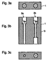
- Figs. 3A, 3B, and 3C are views showing the structure of a dielectric filter according to a third embodiment of the present invention.
- Fig. 3A is a back view of the dielectric filter
- Fig. 3B is a sectional view taken by a surface parallel to a surface to be mounted
- Fig. 3C is a front view of the dielectric filter.
- a resonance line hole 2b has stepped parts in two positions in the axial direction thereof. In this way, by widening the inner diameters near both open-circuited ends of the resonance line hole 2b, the resonance frequency of a resonance line 5b is lowered, and the capacitive coupling between resonators can be enhanced.
- Figs. 4A, 4B, and 4C are views showing the structure of a dielectric filter according to a fourth embodiment of the present invention.
- Fig. 4A is a back view of the dielectric filter
- Fig. 4B is a sectional view taken by a surface parallel to a surface to be mounted
- Fig. 4C is a front view of the dielectric filter.
- coupling electrodes 6a and 7a and coupling electrodes 6b and 7b continued from resonance lines 5a and 5b.
- a capacitance is generated between the coupling electrodes 6a and 6b, and a capacitance is also generated between the coupling electrodes 7a and 7b.
- the inner diameter of the resonance line hole 2a is changed through two phases.
- Figs. 5A, 5B, and 5C are views showing the structure of a dielectric filter according to a fifth embodiment of the present invention.
- an outer conductor 3 is disposed on an opening face of each of resonance line holes 2a and 2b.
- Electrodeless portions g are formed on the inner surfaces of the resonance line holes 2a and 2b near the opening faces. On the other opening faces thereof, no outer conductor 3 is disposed so that the other opening faces are open-circuited.
- each resonance line holes when one of the opening faces of each resonance line holes is an open-circuited end, and a stray capacitance is formed on the other opening face thereof, the resonance lines similarly serve as half-wavelength resonators.
- a coupling electrode as shown in Figs. 4A to 4C may be formed, and a stray capacitance generated by an electrodeless portion may be formed near the other opening face of the resonance line hole.
- Figs. 6A, 6B, and 6C are views showing the structure of a dielectric filter according to a sixth embodiment of the present invention.
- Fig. 6A is a back view of the dielectric filter
- Fig. 6B is a sectional view taken by a surface parallel to a surface to be mounted
- Fig. 6C is a front view of the dielectric filter.
- a dielectric block 1 inside a dielectric block 1, three resonance line holes 2a, 2b, and 2c are disposed.
- One of the opening faces of each of the resonance line holes 2a, 2b, and 2c is an open-circuited end, and an electrodeless portion g is disposed near the other opening face.
- the directions of the resonance line holes 2a, 2b, and 2c are alternately changed in such a manner that the open-circuited-face sides and electrodeless portion sides of the adjacent resonance line holes are opposed to each other. This arrangement increases the level of freedom in a pitch between the resonators.
- terminal electrodes are formed to generate a capacitance between the terminal electrodes and parts near the electrodeless portions g of the resonance lines 5a and 5c. These terminal electrodes are used as an input terminal and an output terminal. With such an arrangement, a dielectric filter showing band pass characteristics formed of three resonators can be obtained.
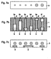
- a seventh embodiment an example of a dielectric duplexer will be illustrated with reference to Figs. 7A, 7B, and 7C.
- Fig. 7A shows a back view of the dielectric filter
- Fig. 7B shows a sectional view taken by a surface parallel to a circuit board to be mounted
- Fig. 7C shows a front view of the dielectric filter.
- resonance line holes 2a to 2f are formed inside a dielectric block 1, resonance line holes 2a to 2f are formed. The diameter of a specified part of each of the resonance line holes 2a to 2f is changed, and an electrodeless portion g is disposed near each of the opening faces of the resonance line holes.
- an outer conductor 3 is formed on the six outer surfaces of the dielectric block 1.
- the terminal electrodes 8 and 9 generate a capacitance between them and parts near the one-side open-circuited ends of the resonance line holes 2a and 2f.
- the terminal electrode 9 is formed to generate a capacitance between the electrode 9 and parts near the one-side open-circuited ends of the resonance line holes 2c and 2d.
- the three resonators formed by the resonator line holes 2a, 2b, and 2c constitute a transmitting side filter having band pass filter characteristics.
- the three resonators formed by the resonance line holes 2d, 2e, and 2f constitute a receiving side filter having band pass characteristics.
- the terminal electrode 8 is used as a Tx terminal
- the terminal electrode 9 is used as an ANT terminal
- the terminal electrode 10 is used as an Rx terminal.
- Figs. 8a, 8B, and 8C are views showing the structure of a dielectric duplexer according to an eighth embodiment of the present invention.
- Fig. 8A is a back view of the dielectric duplexer
- Fig. 8B is a sectional view taken by a surface parallel to a circuit board to be mounted
- Fig. 8C is a front view of the dielectric duplexer.
- a coupling line hole 11 is formed inside a dielectric block 1, in addition to resonance line holes 2a to 2f.
- the coupling line hole 11 couples to resonators formed by the adjacent resonance line holes 2c and 2d.
- a terminal electrode 9 continued from the inner-surface electrode of the coupling line hole 11 is formed.
- One opening face of each of the resonance line holes 2a to 2f is an open-circuited end, and an electrodeless portion is disposed near the other opening face thereof.
- a terminal electrode 8 is formed to generate a capacitance between the terminal electrode 8 and a part near the open-circuited end opened at the electrodeless portion of the resonance line hole 2a, and a terminal electrode 10 is formed to generate a capacitance between the terminal electrode 10 and a part near one of the open-circuited ends of the resonance line hole 2f.
- three resonators formed by the resonance line holes 2a, 2b, and 2d constitute a transmitting side filter having band pass filter characteristics.
- the three resonators formed by the resonance line holes 2d, 2e, and 2f constitute a receiving side filter having the band pass characteristics.
- the terminal electrode 8 is used as a Tx terminal
- the terminal electrode 9 is used as an ANT terminal
- the terminal electrode 10 is used as an Rx terminal.
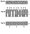
- Figs. 9A, 9B, and 9C are views showing the structures of a dielectric duplexer according to a ninth embodiment of the present invention.
- Fig. 9A is a back view of the dielectric duplexer.
- Fig. 9B is a sectional view taken by a surface penetrating the resonance line holes and the coupling line holes inside a dielectric block 1.
- Fig. 9C is a front view of the dielectric duplexer.
- resonance line holes 2a to 2f and coupling line holes 11 to 13 are formed inside the dielectric block 1. Opening faces of each of the resonance line holes 2a to 2f are open-circuited ends.
- One-side opening faces of the coupling line holes 11 to 13 are open-circuited ends, and, on the other opening faces thereof, terminal electrodes 8, 9, and 10 continued from the inner surface electrode of the holes 11 to 13 are formed.
- the coupling line hole 11 couples to the adjacent resonance line holes 2c and 2d.
- the inner electrode of the resonance line hole 12 couples to the resonance lines of the adjacent resonance line holes 2a and 2b.
- the inner electrode of the coupling line hole 13 couples to the resonance lines of the adjacent resonance line holes 2e and 2f.
- the resonators formed by the resonance line holes 2a and 2f are used as trap resonators.
- the two resonators formed by the resonance line holes 2b and 2c are used as a transmitting side filter.
- the two resonators formed by the resonance line holes 2d and 2e are used as a receiving side filter.
- the resonance frequency of the trap resonator formed by the resonance line hole 2a is set to be a frequency within a reception band or a frequency adjacent to the reception band.
- the resonance frequency of the trap resonator formed by the resonance line hole 2f is set to be a frequency within a transmission band or a frequency adjacent to the transmission band.
- the terminal electrode 8 is used as a Tx terminal
- the terminal electrode 9 is used as an ANT terminal
- the terminal electrode 10 is used as an Rx terminal.
- the structure of the dielectric filter according to a tenth embodiment of the present invention will be illustrated with reference to Fig. 10.
- the resonance lines are disposed inside the dielectric block.
- the reference numeral 21 denotes a dielectric plate.
- resonance lines 5a and 5b are formed on the upper surface of the dielectric plate 21, resonance lines 5a and 5b are formed. The widths of the resonance lines 5a and 5b are changed in specified positions in the longitudinal directions of the resonance lines 5a and 5b to form stepped parts.
- An outer conductor 3 is formed on the upper surface of the dielectric plate 21 and the side surfaces thereof parallel to the resonance lines 5a and 5b.
- terminal electrodes 4a and 4b separated from the outer conductor 3 are formed on outer surfaces of the dielectric block 1. These terminal electrodes 4a and 4b form a capacitance between them and parts near the one-side open-circuited ends of the resonance lines 5a and 5b to make capacitive coupling.
- the dielectric plate 21, the resonance lines 5a and 5b, and the outer conductor 3 constitute two half-wavelength resonators.
- the dielectric filter of the structure shown in each of Figs. 1A and 1B is modified into a dielectric filter using a dielectric plate.
- any of the dielectric filter and the dielectric duplexer shown in Figs. 2 to 9 may be modified into filters and duplexers incorporating dielectric plates.
- the reference character ANT denotes a transmission/reception antenna
- the reference character DPX denotes a duplexer
- the reference characters BPFa, BPFb, and BPFc denote band pass filters
- the reference characters AMPa and AMPb denote amplifying circuits
- the reference characters MIXa and MIXb denote mixers
- the reference character OSC denotes an oscillator
- the reference character DIV denotes a frequency divider (synthesizer).
- the MIXa modulates a frequency signal output from the DIV by a modulation signal.
- the BPFa passes only the signal of a transmission frequency band
- the AMPa power-amplifies the signal to transmit from the ANT via the DPX.
- the BPFb passes only the signal of a reception frequency band among signals output from the DPX, and the AMPb amplifies the passed signal.
- the MIXb mixes a frequency signal output from the BPFc and the received signal to output an intermediate frequency signal
- the duplexer DPX shown in Fig. 11 the duplexer having the structure shown in each of Figs. 7 to 9 is used.
- the band pass filters BPFa, BPFb, and BPFc the dielectric filter having the structure shown in each of Figs. 1A to 6C and Fig. 10 is used.
- an antenna duplexer having desired filter characteristics of both the transmitting side filter and the receiving side filter can be formed.
Landscapes
- Physics & Mathematics (AREA)
- Electromagnetism (AREA)
- Control Of Motors That Do Not Use Commutators (AREA)
Abstract
Description
Claims (3)
- A dielectric filter comprising:a plurality of resonance lines (5a, 5b, 5c) substantially parallel to each other arranged on an upper surface of a dielectric substrate (21) or inside a dielectric block (1); andan outer conductor (3) formed on the lower surface of the dielectric substrate (21) or on an outer surface of the dielectric block (1);
wherein both ends of each of the plurality of resonance lines (5a, 5b, 5c) or parts near both ends thereof are open-circuited, and the size of the width of at least one of the resonance lines (5a, 5b, 5c) is changed in at least one position in the longitudinal direction of the resonance line (5a, 5b, 5c) to form a stepped part. - A dielectric duplexer comprising:the dielectric filter according to Claim 1 formed on a single dielectric plate or in a single dielectric block (1) to be used as each of a transmitting side filter and a receiving side filter;a transmitted-signal input terminal coupled to a first-stage resonance line of the transmitting side filter;a received-signal output terminal coupled to a last-stage resonance line of the receiving side filter; andan antenna terminal coupled to a last-stage resonance line of the transmitting side filter and a first-stage resonance line of the receiving side filter, respectively.
- A communication apparatus comprising one of the dielectric filter according to Claim 1 and the dielectric duplexer according to Claim 2.
Priority Applications (1)
| Application Number | Priority Date | Filing Date | Title |
|---|---|---|---|
| EP05021531A EP1612881B1 (en) | 1999-10-13 | 2000-10-04 | Dielectric filter, dielectric duplexer, and communication apparatus incorporating the same |
Applications Claiming Priority (2)
| Application Number | Priority Date | Filing Date | Title |
|---|---|---|---|
| JP29157899A JP3574893B2 (en) | 1999-10-13 | 1999-10-13 | Dielectric filter, dielectric duplexer and communication device |
| JP29157899 | 1999-10-13 |
Related Child Applications (1)
| Application Number | Title | Priority Date | Filing Date |
|---|---|---|---|
| EP05021531A Division EP1612881B1 (en) | 1999-10-13 | 2000-10-04 | Dielectric filter, dielectric duplexer, and communication apparatus incorporating the same |
Publications (3)
| Publication Number | Publication Date |
|---|---|
| EP1093179A2 true EP1093179A2 (en) | 2001-04-18 |
| EP1093179A3 EP1093179A3 (en) | 2002-03-27 |
| EP1093179B1 EP1093179B1 (en) | 2006-05-17 |
Family
ID=17770750
Family Applications (2)
| Application Number | Title | Priority Date | Filing Date |
|---|---|---|---|
| EP05021531A Expired - Lifetime EP1612881B1 (en) | 1999-10-13 | 2000-10-04 | Dielectric filter, dielectric duplexer, and communication apparatus incorporating the same |
| EP00121700A Expired - Lifetime EP1093179B1 (en) | 1999-10-13 | 2000-10-04 | Dielectric filter, dielectric duplexer and communication apparatus incorporating the same |
Family Applications Before (1)
| Application Number | Title | Priority Date | Filing Date |
|---|---|---|---|
| EP05021531A Expired - Lifetime EP1612881B1 (en) | 1999-10-13 | 2000-10-04 | Dielectric filter, dielectric duplexer, and communication apparatus incorporating the same |
Country Status (6)
| Country | Link |
|---|---|
| US (2) | US6833773B1 (en) |
| EP (2) | EP1612881B1 (en) |
| JP (1) | JP3574893B2 (en) |
| KR (1) | KR100411203B1 (en) |
| CN (1) | CN1160825C (en) |
| DE (2) | DE60043316D1 (en) |
Cited By (1)
| Publication number | Priority date | Publication date | Assignee | Title |
|---|---|---|---|---|
| CN112954745A (en) * | 2019-12-10 | 2021-06-11 | 成都鼎桥通信技术有限公司 | Wide-narrow dual-mode cluster terminal and mode switching method and device thereof |
Families Citing this family (6)
| Publication number | Priority date | Publication date | Assignee | Title |
|---|---|---|---|---|
| JP3405316B2 (en) * | 2000-03-27 | 2003-05-12 | 松下電器産業株式会社 | High frequency switch |
| AU2003220104A1 (en) * | 2002-03-08 | 2003-09-22 | Conductus, Inc. | Resonator and coupling method and apparatus for a microstrip filter |
| JP2009206506A (en) * | 2008-01-31 | 2009-09-10 | Sanyo Electric Co Ltd | Substrate for mounting element and its manufacturing method, semiconductor module and portable device mounted with the same |
| CN104241801A (en) * | 2014-09-16 | 2014-12-24 | 张家港保税区灿勤科技有限公司 | Dielectric resonator with reverse step type resonant cavity and working method thereof |
| US9941563B2 (en) | 2014-09-30 | 2018-04-10 | Skyworks Solutions, Inc. | Ceramic filter using stepped impedance resonators having an inner cavity with at least one step and taper |
| CN106785262B (en) * | 2017-01-18 | 2021-03-12 | 苏州富电通讯有限公司 | Medium interdigital filter |
Family Cites Families (19)
| Publication number | Priority date | Publication date | Assignee | Title |
|---|---|---|---|---|
| US4371853A (en) * | 1979-10-30 | 1983-02-01 | Matsushita Electric Industrial Company, Limited | Strip-line resonator and a band pass filter having the same |
| JPS5895403A (en) * | 1981-12-01 | 1983-06-07 | Matsushita Electric Ind Co Ltd | Coaxial dielectric resonator |
| US4985690A (en) * | 1988-07-07 | 1991-01-15 | Matsushita Electric Industrial Co., Ltd. | Dielectric stepped impedance resonator |
| JPH0292001A (en) | 1988-09-28 | 1990-03-30 | Murata Mfg Co Ltd | Dielectric coaxial filter |
| KR0174531B1 (en) * | 1989-11-20 | 1999-04-01 | 이우에 사또시 | Band-passfilter using microstrip lines and filter characteristic adjusting method thereof |
| JP2910807B2 (en) * | 1991-10-25 | 1999-06-23 | 株式会社村田製作所 | Dielectric resonator device, dielectric filter, and method of manufacturing the same |
| US5475350A (en) * | 1992-09-29 | 1995-12-12 | Matsushita Electric Industrial Co., Ltd. | Frequency tunable resonator including a varactor |
| JPH06216605A (en) * | 1992-11-27 | 1994-08-05 | Sanyo Electric Co Ltd | Stripline filter |
| JP3239552B2 (en) * | 1993-09-16 | 2001-12-17 | 株式会社村田製作所 | Dielectric resonator device |
| JPH0794911A (en) * | 1993-09-20 | 1995-04-07 | Murata Mfg Co Ltd | Dielectric resonator device |
| JP3254866B2 (en) * | 1993-12-21 | 2002-02-12 | 株式会社村田製作所 | Dielectric resonator and method of manufacturing the same |
| JP3307044B2 (en) * | 1993-12-24 | 2002-07-24 | 松下電器産業株式会社 | Dielectric resonator and its input / output coupling circuit |
| JP3211547B2 (en) * | 1994-01-25 | 2001-09-25 | 株式会社村田製作所 | Dielectric filter |
| JP3158963B2 (en) | 1995-05-31 | 2001-04-23 | 株式会社村田製作所 | Antenna duplexer |
| US5684439A (en) * | 1995-10-10 | 1997-11-04 | Motorola, Inc. | Half wave ceramic filter with open circuit at both ends |
| EP0851526B1 (en) * | 1996-12-27 | 2003-07-30 | Murata Manufacturing Co., Ltd. | Filtering device |
| JP3577921B2 (en) * | 1997-01-13 | 2004-10-20 | 株式会社村田製作所 | Dielectric filter and dielectric duplexer |
| JPH10224111A (en) | 1997-02-10 | 1998-08-21 | Murata Mfg Co Ltd | Dielectric filter and method for setting its external connection q |
| JP3633280B2 (en) * | 1998-05-29 | 2005-03-30 | 松下電器産業株式会社 | Half-wave resonator type high frequency filter |
-
1999
- 1999-10-13 JP JP29157899A patent/JP3574893B2/en not_active Expired - Lifetime
-
2000
- 2000-10-04 DE DE60043316T patent/DE60043316D1/en not_active Expired - Lifetime
- 2000-10-04 EP EP05021531A patent/EP1612881B1/en not_active Expired - Lifetime
- 2000-10-04 EP EP00121700A patent/EP1093179B1/en not_active Expired - Lifetime
- 2000-10-04 DE DE60027982T patent/DE60027982T2/en not_active Expired - Lifetime
- 2000-10-11 KR KR10-2000-0059743A patent/KR100411203B1/en not_active Expired - Lifetime
- 2000-10-12 CN CNB001329103A patent/CN1160825C/en not_active Expired - Lifetime
- 2000-10-13 US US09/687,903 patent/US6833773B1/en not_active Expired - Lifetime
-
2002
- 2002-10-08 US US10/265,741 patent/US6822538B2/en not_active Expired - Lifetime
Cited By (2)
| Publication number | Priority date | Publication date | Assignee | Title |
|---|---|---|---|---|
| CN112954745A (en) * | 2019-12-10 | 2021-06-11 | 成都鼎桥通信技术有限公司 | Wide-narrow dual-mode cluster terminal and mode switching method and device thereof |
| CN112954745B (en) * | 2019-12-10 | 2023-04-28 | 成都鼎桥通信技术有限公司 | Wide-narrow dual-mode cluster terminal and mode switching method and device thereof |
Also Published As
| Publication number | Publication date |
|---|---|
| EP1612881A2 (en) | 2006-01-04 |
| CN1303137A (en) | 2001-07-11 |
| DE60027982D1 (en) | 2006-06-22 |
| US6833773B1 (en) | 2004-12-21 |
| JP2001111304A (en) | 2001-04-20 |
| US20030025578A1 (en) | 2003-02-06 |
| JP3574893B2 (en) | 2004-10-06 |
| EP1612881B1 (en) | 2009-11-11 |
| EP1093179B1 (en) | 2006-05-17 |
| US6822538B2 (en) | 2004-11-23 |
| EP1612881A3 (en) | 2008-02-20 |
| EP1093179A3 (en) | 2002-03-27 |
| DE60043316D1 (en) | 2009-12-24 |
| KR20010050956A (en) | 2001-06-25 |
| CN1160825C (en) | 2004-08-04 |
| DE60027982T2 (en) | 2006-12-28 |
| KR100411203B1 (en) | 2003-12-18 |
Similar Documents
| Publication | Publication Date | Title |
|---|---|---|
| EP1045469B1 (en) | Dielectric filter, dielectric duplexer and communication apparatus | |
| EP0986124B1 (en) | Dielectric filter, composite dielectric filter, antenna duplexer, and comunication apparatus | |
| EP1001479B1 (en) | Dielectric filter, duplexer, and communication apparatus | |
| EP1612881B1 (en) | Dielectric filter, dielectric duplexer, and communication apparatus incorporating the same | |
| EP0986125B1 (en) | Dielectric filter, composite dielectric filter, duplexer, and communication apparatus | |
| KR100343320B1 (en) | Dielectric Filter, Dielectric Duplexer, and Communication Apparatus Using The Same | |
| EP1180813B1 (en) | Dielectric filter with external coupling electrodes | |
| EP1294042B1 (en) | Dielectric filter, dielectric duplexer, and communication device | |
| KR100338589B1 (en) | Dielectric Filter, Dielectric Duplexer, and Communication Apparatus | |
| US6580339B2 (en) | Dielectric duplexer and communication apparatus | |
| JP2000138502A (en) | Dielectric filter, duplexer, and communication device |
Legal Events
| Date | Code | Title | Description |
|---|---|---|---|
| PUAI | Public reference made under article 153(3) epc to a published international application that has entered the european phase |
Free format text: ORIGINAL CODE: 0009012 |
|
| 17P | Request for examination filed |
Effective date: 20001004 |
|
| AK | Designated contracting states |
Kind code of ref document: A2 Designated state(s): AT BE CH CY DE DK ES FI FR GB GR IE IT LI LU MC NL PT SE Kind code of ref document: A2 Designated state(s): DE FR GB |
|
| AX | Request for extension of the european patent |
Free format text: AL;LT;LV;MK;RO;SI |
|
| PUAL | Search report despatched |
Free format text: ORIGINAL CODE: 0009013 |
|
| AK | Designated contracting states |
Kind code of ref document: A3 Designated state(s): AT BE CH CY DE DK ES FI FR GB GR IE IT LI LU MC NL PT SE |
|
| AX | Request for extension of the european patent |
Free format text: AL;LT;LV;MK;RO;SI |
|
| AKX | Designation fees paid |
Free format text: DE FR GB |
|
| 17Q | First examination report despatched |
Effective date: 20030219 |
|
| GRAP | Despatch of communication of intention to grant a patent |
Free format text: ORIGINAL CODE: EPIDOSNIGR1 |
|
| GRAS | Grant fee paid |
Free format text: ORIGINAL CODE: EPIDOSNIGR3 |
|
| GRAA | (expected) grant |
Free format text: ORIGINAL CODE: 0009210 |
|
| AK | Designated contracting states |
Kind code of ref document: B1 Designated state(s): DE FR GB |
|
| REG | Reference to a national code |
Ref country code: GB Ref legal event code: FG4D |
|
| REF | Corresponds to: |
Ref document number: 60027982 Country of ref document: DE Date of ref document: 20060622 Kind code of ref document: P |
|
| ET | Fr: translation filed | ||
| PLBE | No opposition filed within time limit |
Free format text: ORIGINAL CODE: 0009261 |
|
| STAA | Information on the status of an ep patent application or granted ep patent |
Free format text: STATUS: NO OPPOSITION FILED WITHIN TIME LIMIT |
|
| 26N | No opposition filed |
Effective date: 20070220 |
|
| REG | Reference to a national code |
Ref country code: FR Ref legal event code: PLFP Year of fee payment: 16 |
|
| REG | Reference to a national code |
Ref country code: FR Ref legal event code: PLFP Year of fee payment: 17 |
|
| REG | Reference to a national code |
Ref country code: FR Ref legal event code: PLFP Year of fee payment: 18 |
|
| REG | Reference to a national code |
Ref country code: FR Ref legal event code: PLFP Year of fee payment: 19 |
|
| PGFP | Annual fee paid to national office [announced via postgrant information from national office to epo] |
Ref country code: DE Payment date: 20191021 Year of fee payment: 20 |
|
| PGFP | Annual fee paid to national office [announced via postgrant information from national office to epo] |
Ref country code: FR Payment date: 20191028 Year of fee payment: 20 |
|
| PGFP | Annual fee paid to national office [announced via postgrant information from national office to epo] |
Ref country code: GB Payment date: 20191021 Year of fee payment: 20 |
|
| REG | Reference to a national code |
Ref country code: DE Ref legal event code: R071 Ref document number: 60027982 Country of ref document: DE |
|
| REG | Reference to a national code |
Ref country code: GB Ref legal event code: PE20 Expiry date: 20201003 |
|
| PG25 | Lapsed in a contracting state [announced via postgrant information from national office to epo] |
Ref country code: GB Free format text: LAPSE BECAUSE OF EXPIRATION OF PROTECTION Effective date: 20201003 |